Note: Descriptions are shown in the official language in which they were submitted.
~lZ863'~2
PRECISE PHASE START-UP VOLTAGE CONTROLLED
OSCILLATOR WITH ACCURATE D~TY CYCLE
BACKGROUND OF THE INVENTION
1. Field of the Invention
The present invention relates to voltage
controlled oscillators and more particularly to voltage
controlled oscillators intended for use in phase-locked
loop systems. Still more particularly, the present
invention is directed to a voltage controlled oscillator
10 for use in a phase-locked loop data separation circuit
for use in disc drive systems.
Typically, information is recorded on magnetic
discs in disc drive systems in the form of data pulses
combined with clock puises. In order to read
15 information from the disc, signals from a magnetic head
are applied to a data synchronization circuit which
generates a recovered clock signal based upon the
detection of data and clock pulses. The recovered clock
signal corresponds to the pulse rate of the signals read
20 from the disc and is used to separate the data and clock
pulses. The generation of the recovered clock signal is
accomplished by means of a phase-locked loop system.
The phase-locked loop system typically employs a voltage
controlled oscillator which is controlled so as to
25 generate an output signal having a frequency equal to
the data rate. The input to the voltage controlled
oscillator is a control signal representative of the
phase error between the incoming signal from the disc
and the output of the phase-locked loop.
. . . - .
.,, . , . ~:
.
lZ86372
--2--
2. Description of_the Prior Art
Prior art voltage controlled oscillators for use
in data separators have typically been comprised of an
inverting amplifier connected to a resonant feedback
5 network such as an LC network. A varactor forms part of
the feedback network and the voltage applied to the
varactor determines the oscillation frequency. The
output of the amplifier is the oscillator output.
Although generally acceptable, such oscillators have
10 several drawbacks. First, the duty cycle of the
oscillator is not balanced, i.e., the high and low
signal levels for each cycle are not of equal duration.
Secondly, such oscillators typically have a start-up
delay before they reach the desired operating phase due
15 to small, slowly increasing amplitude of the
oscillations.
'
'
:.
~:~86372
--3
SU MMARY OF TH E I NV ENT ION
The present invention is directed to a voltage
controlled oscillator which provides an extremely
precise d~ty cycle and which is controllable so that it
5 will start precisely in phase with an input signal. The
provision of an output signal having a 50% duty cycle
enables the signal to be used to control data
synchronization functions which otherwise would have to
be controlled in a different fashion. The oscillator
10 includes an inverting amplifier and a resonant network
feedback loop. The inverting amplifier oscillates
between a high and low level depending on the value of
its input from the resonant network. The input to the
inverting amplifier is also connected to a comparator
15 having a reference voltage applied to it which is
pcecisely equal to the threshold voltage of the
inverting amplifier. Since the input to the amplifier
is a very precise sine wave centered about the threshold
voltage of the amplifier, the output of the comparator
20 will be a precise square wave having a 50~ duty cycle.
The comparator output functions as the output of the
oscillator.
In addition to providing an output having a So~
duty cycle, the oscillator of the present invention
25 includes circuitry to ensure that the oscillator output
will start-up precisely in phase with an input signal.
This is accomplished by including a transistor which
connects the resonant network to a supply voltage to
preset the output of the oscillator. In order to start
30 the oscillator, the supply voltage is disconnected from
the resonant network, thus allowing oscillations to
commence at the desired frequency and phase.
.. . . .
. ~ . .
- ' . .' ' ' : . ' . - -:
: .. ,':. ' , . - .
' - ' . ' -- , ~ . ' ' '
- ,
lZ863 ~2
--4--
BRIEF DESCRIPTION OF THE DRAWINGS
The invention will be described with reference to
the accompanying drawings wherein:
Figure 1 is a block diagram of a phase-locked
5 loop system employing the voltage controlled oscillator
of the present invention; and
Figure 2 is a schematic diagram of the voltage
controlled oscillator of the present invention.
, . ~ . - . . . . .
. ~ ~ . . . . . ~ ., , . . . . - .
. .. , - .
. ~ . . . : . . . .
,, , ~ . . - . .
,.. ~. ~ .- . . . .
12863~2
--5--
DESCRIPTION OF THE PREFERRED EMBODIMENT
. _ ... . _ . ~
The following description is of the best
presently contemplated mode of carrying out the
invention. This description is made for the purpose of
S illustratins the general principles of the invention and
is not to be taken in a limiting sense. The scope of
the invention is best determined by reference to the
appended claims.
Referring to Figure 1, a phase detector 12 of a
10 phase-locked loop system 10 receives an input signal
from a multiplexer 14. The input signal is either a
data signal of pulses from a disc drive or a reference
signal from a crystal oscillator. The data rate is
nominally equal to the frequency of the reference. When
15 data is not being received from the disc drive, the
reference signal is applied to the phase-locked loop in
order to have it running at near the desired frequency.
The signal from the multiplexer is compared to an
output signal of the phase-locked loop by the phase
20 detector 12. The output signal is labeled VCO~K. The
phase detector provides an error signal whose duration
is proportional to the phase error between the output
signal and the signal from the multiplexer 14. This
error signal is amplified by an error amplifier 16 and
25 iltered by means of a low pass filter 18 to provide a
control voltage Vc representative of the phase error
between the input to the phase-locked loop and the
output of the phase-locked loop.
The error voltage is applied to a voltage
30 controlled oscillator 20 which provides an output signal
hav~ng a frequency proportional to the input control
voltage. The VCO also receives a CLAMP signal, the
function of which will be described subsequently. The
output signal VCOCLK of the VCO 20 is thus a signal
3S which is phase and frequency locked to the input signal
from the multiplexer 14. During normal operation, the
VCO output will therefore be locked in frequency and
phase with the data input signal. The output signal
VCOCLK is then used to separate data and clock signals
: , - . . .. . : - .
~ .. : - .. :
.. , - . . .
.. , ~ : . -
~- . ' . .
lZ86372
--6--
~rom the signal read from the disc drive. The actual
manner of data separation is not a part of the present
invention and will therefore not be described. However,
it is to be noted that the particular data separation
5 technique employed relies upon an output signal from the
vCo 20 which has a precise duty cycle. The VCO of the
present invention is configured to provide an output
having a very precise duty cycle for such data
separation appl ications.
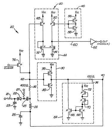
The VCO 20 is shown in detail in Figure 2. The
control voltage Vc is applied via a resistor 21 to one
terminal of a varactor 22 which forms a part of an LC
series resonant network which also includes an inductor
24 and capacitors 23, 25 and 26. A bias voltage to
15 controls the center frequency of the VCO is applied via
a resistor 27. These elements are connected in a
feedback loop of an inverting amplifier 30 via an input
resistor 32 and an output resistor 34, all of which are
monolithically formed. The inverter 30 is formed of a
20 P-type transistor 36 and an N-type transistor 38. The
output of the inverter is of a polarity opposite to its
input, and it will switch at a threshold determined by
the relative channel dimensions of the transistors 36
and 38.
The inverting amplifier 30 in combination with
the positive feedback network forms an oscillator
circuit similar to those employed in prior art systems,
with an output being obtained at point 40. The voltage
applied to the varactor 22 controls the capacitance of
30 the varactor and therefore the frequency obtained at the
point 40. However, the signal obtained at this point
does not have a good duty cycle because of differing
rise and fall times of the inverter, and thus is not
suitable for certain appl ications.
The operation of the inverter 30 and series
resonant circuit is such that the input to the inverter
30 at point 42 will be an extremely precise sine wave
centered about the switching threshold of the inverter.
The frequency of the sine wave is alterable by changing
' ': ~ .
~: -
. . ~ . .
1286372
--7--
the voltage applied to the varactor 22. In order toobtain a square wave having a precise 50% duty cycle,
the signal at point 42 is applied to one input of a
comparator 44 and compared to a reference voltage
5 provided by reference voltage generator 46. The
comparator 44 is comprised of P-type transistors 48 and
50 having their sources connected to a supply voltage
Vcc and N-type transistors 52 and 54 having their drains
connected to the drains of the transistors 48 and 50,
lo respectively, and their sources co~nected to ground.
The reference voltage generator 46 is comprised of a
P-type transistor 56 and an N-type transistor 58 having
their gates and drains interconnected.
Since the signal at point 42 is a sine wave
15 centered about the switching threshold of the inverter
30, a square wave output from the comparator 44 having a
preciEe 50~ duty cycle can be obtained by setting the
reference voltage from the generator 46 equal to the
switching threshold of the inverter 30. This is easily
20 accomplished by fabricating the transistors 56 and 58 so
that their channel dimension ratio is the same as the
channel dimension ratio of the transistors 36 and 38 of
the inverter 30. That is, although the transistor 56
need not be equal in size to the transistor 36 and the
25 transistor 58 need not be equal in size to the
transistor 38, the ratios of the channel dimensions of
the transistors 56 and 58 is the same as the ratio of
the channel sizes of the transistors 36 and 38. The
comparator 44 will thus have a switching threshold
30 precisely equal to the threshold of the inverter 30 and
will be precisely centered with respect to the sine wave
input to the comparator 44. The comparator output on
line 60 will thus be a square wave having a very precise
duty cycle, i.e., high and low levels of equal duration.
35 This output signal is applied to a buffer amplifier 62,
the output of which is the output of the VCO 20.
The dimensions of the channels of the transistors
36 and 38 of the inverter are deliberately selected so
that there is an imbalance between them so as to reduce
- . . .
.
. .
i .
,
lZ863 ~ 2
--8--
power consumption and minimize AC power noise. Thus, in
the present embodiment, the power supply voltage Vcc is
equal to five volts and the threshold voltage of the
inverter 30 is equal to approximately one volt. In
order to further improve the symmetry of the resonant
circuit and therefore the symmetry of the sine wave
applied to the comparator, the output of the inverter 30
is clamped to a level equal to approximately twice the
threshold voltage of the inverter, i.e., to a level of
two volts. Since the minimum level of the inverter
output is zero volts and the threshold is one volt, the
clamping of the output of the inverter to a two volt
level ~as opposed to allowing it to go to the five volt
level of the power supply) further improves the symmetry
of the input sine wave. The clamping is accomplished by
means of a peak limiter 64 which includes a P-type
transistor 66 connected to the output of the inverter
30, an N-type transistor 68 having its gate connected to
its drain and to the gate of the transistor 66 and two
P-type transistors 70 and 72 connected between the
transistor 68 and the power supply. Transistors 68, 70
and 72 form a voltage divider which biases the
transistor 66. The bias is selected so that the
transistor 66 will start conducting when the output of
the inverter 30 is equal to approximately two volts,
i.e., twice the switching threshold of the inverter.
The circuit of Figure 2 also includes elements
which enable the VCO to rapidly achieve steady state
operation and to start-up at a known phase relation with
respect to a control signal. This is accomplished by
the provision of a clamp transistor 74 which serves to
connect the input of the inverting amplifier 30 to the
supply voltage. When the clamp transistor is
conducting, it stores energy in the resonant circuit and
halts the oscillations of the circuit. The clamp
transistor together with output resistor 34 and input
protection resistor 32 (both monolithically formed with
the active devices of the circuit) allow sufficient
energy to be stored in the resonant circuit to aid in
. , . : '
: .. .. -. .. : ,
: . :, . .
- ~ - ', . ' :
,. . . ~ . : .
. . ~ . .
121Y6372
,~,
quick start-up of the oscillator. When the transistor
74 is shut off by removing the drive signal CLAMP from
its base, the energy stored in the resonant circuit
causes a voltage to be reflected to the input of the
inverting amplifier 30 at a predetermined point in the
cycle of the sinusoidal input signal. This enables the
circuit to oscillate almost immediately at substantially
full amplitude.
When the clamp transistor 74 is conducting, the
supply voltage will be applied to the input of the
amplifier 30 and the transistor 38 will be rendered
conductive. The inductor 24 will appear as a short and
the drain to source resistance of the transistor 38 will
be negligible. As a result, voltage across the
capacitor 26 and varactor 22 will be determined by the
relative values of the resistor 32 and resistor 34. In
the described embodient of the invention, the resistor
32 has a value four times that of the resistor 34. With
a supply voltage of five volts, there will be
approximately a four volt drop across the resistor 32
and a one volt drop across the resistor 34. This
provides a constant current through the inductor 24 to
store energy in it. In addition, the capacitor 26 is
charged to approximately a one volt level, as is the
combination of the varactor 22 and capacitors 23 and 25.
When data is to be read, a control circuit (not
shown) will turn off the transistor 74 in
synchronization with a data signal. This disconnects
the supply voltage from the input of the inverting
amplifier 30. Since energy is stored in the capacitor
26 and the series combination of the capacitors 23 and
25 and the varactor 22, the one volt level across them
will be applied to the input of the inverting amplifier
30. This one volt level is approximately the threshold
voltage of the amplifier 30, and oscillations at the
steady state level will begin almost immediately. By
varying the relative values of the resistors 32 and 34,
the start-up phase may be selectively controlled.
., ,, :
. .
.:
.. .. . .
., ~ i
~2~;3'7Z
--10--
In summary, the present invention provides a
voltage controlled oscillator which has a precise 50~
duty cycle and which is controllable to start up in a
predetermined phase at substantially steady state
operation. The oscillator is therefore ideally suited
for use in a phased-lock loop of a data separator for
magnetic discs.