Note: Descriptions are shown in the official language in which they were submitted.
121364~
TITLE OF THE INVENTION
METHOD AND APPARAl'US FO~ T~ANSMITTING
AND/OR RECEIVING A DIGITAL SIGNAL
EIELD OF THE INVENTION
The present invention relates to a digital tape
recorder and, more particularly, to a method and
apparatus for transmitting and/or receiving a digital
signal in a rotary head type digital tape recorder.
DESCRIPTION OF RELATED BACKGROUND ART
There has been proposed a rotary head type digital
tape recorder for recording/reproducing a digital audio
signal (PCM signal) by a pair of rotary heads. In such
a digital tape recorder, sub codes such as the program
number, the time code, and the like are recorded. In
addition, PCM-IDs for identifying the sampling
fre~uency, the number of channels, and the number of
digitization bits of the PCM signal, the presence or
absence of preemphasis, the characteristic thereof, and
the like are recorded together with the PCM signal.
In the proposed digital tape recorder, the PCM
signal can be input and output in the form of serial
data in order to be able to supply an analog audio
signal as the recording input signal, to obtain an
analog audio signal as the reproduction output signal,
and to make it possible to easily digitally couple with
other PCM apparatuses such as other digital tape
recorders, digital mixers, and the like. In this case,
it is necessary to transmit the sub data together with
the PCM signal. Several ~ormats have been proposed by
EBU, Philips, and others as standards for the PCM signal
transmitting systems. According to the format of EBU,
the auxiliary bits of four bits and the user data of one
bit for the sub code of the compact disc are assigned to
. ' , ' ' . ' ': ' '
.
.
' ' ' ' ', ;' ' , '' .:
.
~2~36~
one audio sample data. According to the format of
Philips, the PCM signal and the other data are
multiplexed when transmitted and received.
In the ca~e of the proposed rotary head type
digital tape recorder, there is a large amount of sub
data of the sub codes and PCM-ID. Therefore, the sub
data cannot be transmitted by any of these conventional
PCM signal transmitting systems.
SUMMARY OF THE INVENTION
It is, therefore, an object of the present
invention to provide a method and apparatus for
transmitting and/or receiving a digital signal in a
rotary head type digital tape recorder in which a large
amount of sub data can be input and output toget~er with
the PCM signal as compared with a compact disc or the
like.
According to the invention, there is provided a
method and apparatus for transmitting and/or receiving a
digital signal in a rotary head type digital tape
recorder in which a PCM signal and sub data relating to
control and the like of the PCM signal are recorded or
reproduced kogether by rotary heads. Serial data, with
each symbol of the sub data and every word of the PCM
signal being transmitted as a pair, can be input and
output for the period of time corresponding to a
predetermined number of symbols in the pulse signal
which are synchronized with the rotation of the rotary
heads.
The recording data or reproduced data input or
output with respect to the rotary heads is transmitted
as serial data for a predetermined period of time which
is equal to the scanning interval of the rotary heads.
For the period of time corresponding to a predetermined
number of words (472 word~i) within the faregoing
.. .. . . . . .
:' '
-
~ (t~
predetermined period of time, each symbol (eight bits)
of the sub data is transmitted as a pair with each word
(sixteen bits) of the PCM signal. Therefore, the 472
symbols can be input and output as serial data together
with the PCM signal.
The above and other objects and features of the
present invention will become apparent from the
following detailed descrip~ion and the appended claims
with reference to the accompanying drawings.
BRIEF DESCRIPTION OF TXE DRAWINGS
Fig. 1 is a block diagram showing an overall
constitution of a rotary head type digital tape recorder
to which the present invention can be applied;
Fig. 2 is a schematic diagram showing a tape format
of the digital tape recorder;
Figs. 3A to 3E are schematic diagrams for
explaining a track format and a block format o~ the
digital tape recorder;
Figs. 4A and 4B are schematic diagrams for
explaining error correction codes of the digital tape
recorder;
Fig. 5 is a block diagram of the main section of an
embodiment of the invention;
Figs. 6 and 7 are time charts for explaining the
reproducing and recording modes of transmission data;
Figs. 8 to 10 are schematic diagrams for explaining
the sub data; and
Fig. 11 is a time chart for explaining the
transmission data.
DESCRIPTION OF THE_ REFE_RED EMBODIMENT
An embodiment when the present invention is applied
to a rotary head type digital tape recorder
(hereina~ter, abbreviated to an RDAT) will be described
' ' -
, .
6~
in detail hereinbelow with reference to the drawings in
accordance with the followiny order.
a. Overall constitution of a digital tape recorder;
b. Data constitution of a digital tape recorder;
c. Error correction codes of a digital tape recorder;
d. Recording signal processor and reproduction signal
processor according to the present invention; and
e. Data transferring system according to the present
invention .
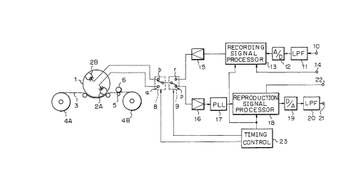
a. Overall constitution of a digital tape recorder:
Fig. 1 shows an overall constitution of a rotary
head type digital tape recorder (i.e., RDAT) for use
with the present invention. In the diagram, reference
numeral 1 denotes a drum having a diameter of 3Omm which
is rotated at a speed of 2000 r.p.m. A pair of magnetic
heads 2A and 2B are attached to the drum 1 with an
angular interval of 180. A magnetic tape 3 (indicated
by an alternate long and short dash line) is obliquely
wound around the peripheral surface of the drum 1 at a
wrap angle of 90. The magnetic tape 3 is laid between
reel hubs 4A and 4B of a tape cassette and is moved at a
speed of 8.15 mm/sec by a capstan 5 and a pinch roller
6.
As the drum 1 is rotated, the magnetic heads 2A and
2B alternately come into contact with the magnetic tape
3, thereby forming oblique tracks 7A and 7B onto the
magnetic tape 3 as shown in Fig. 2. A tape width A of
the magnetic tape 3 is 3.81 mm. The magnetic gap of the
rotary head 2A is inclined by an angle of inclination of
+~ with respect to the direction perpendicular to the
track. The magnetic gap of the other rotary head 2B is
inclined by an angle of inclination of -~ with regard to
the direction perpendicular to the track. The value of
is set to 20. The angles of the magnetic gaps o~ the
~z~o~
_ 5 _
magnetic heads 2A and 2B are called + azimuth and -
azimuth, respectively.
The magnetic heads 2A and 2B are alternately
selected by a head change-over switch 8. The recording
signal from a terminal r of a recording/reproducing
switch 9 is supplied to the magnetic heads 2A and 2B
through rotary transformers (not shown). The reproduced
signals of the magnetic heads 2A and 2B are taken out to
a terminal p of the switch 9 through the rotary
transformers (not shown).
The analog audio signal from an input terminal 10
is supplied to an A/D converter 12 through a low pass
4ilter 11 and converted into a digital audio signal (at
a sampling frequency of 48 kHz on the basis of a linear
digitization of 16 bits). The digital audio signal from
the A/D conver~er 12 is supplied to a recording signal
processor 13. In the processor 13, the digital audio
signal is subjected to an error correction coding
process and converted into the format o~ ~he recording
data, which will be explained hereinafter. In this
case, an ID signal (PCM-ID) to identify the on/off of
the preemphasis of the signal to be recorded, the
sampling frequency, the number of digitization bits, and
the like is added. The sub codes such as the program
number, the time code, and the like of the signal to be
recorded, and an ID signal (sub code ID) for the sub
codes are formed by a sub code encoder (not shown) and
supplied from a terminal 14 to the recording signal
processor 13.
Serial recording data for each track is generated
from the processor 13 synchronously with the rotation of
the magnetic heads 2A and 2B. The recording data is
supplied to the head change-over switch 8 through a
recording amplifier 15 and the terminal r of the
recording/reproducing switch 9. The recording data is
- j ~, .
.
', : :
.
:,. :,
.- :
.
~6~0~
- 6 -~ -
alternately supplied to the magnetic heads 2A and 2~ by
the switch 8.
During reproduction, the signals reproduced by the
magnetic heads 2A and 2B are supplied to a reproducing
amplifier 16 through the switch 8 and through a terminal
p of the switch 9. The output signal of the reproducing
amplifier 16 is supplied to a phase locked loop (PLL~
17. In the PLL 17, the clock signal synchronized with
the reproduced signal is extracted. In a reproduction
signal processor 18, the reproduced signal from the PLL
17 is subjected to the processes of error correction,
interpolat~on, and the like. The reproduced digital
audio signal is supplied to a D/A converter 19. The
reproduced audio signal from the D/A converter 19 is
taken out to an output terminal 21 through a low pass
filter 20. Further, the sub codes and sub code ID are
separated by the reproduction signal processor 18 and
taken out to an output terminal 22. A sub code decoder
(not shown) is connected to the output terminal 22 and
control data and the like are formed from the sub codes.
Control signals to control the head change-over
switch 8 and recording/reproducing change-over switch 9
are formed by a timing controller 23 from a PG pulse
indicative of the rotation of the heads. In addition,
the timing controller 23 generates cloc]c signals and
timing signals which are respectively necessary for the
recording signal processor li and reproduction signal
processor 18 using the c].ock signal, block sync siynal,
and the like from the PLL 17.
b. Data constitution of a digital tape recorder:
The whole part of the data to be recorded in a
single track is called one segment. Fig. 3A shows a
constitution of the data of one segment which is
recorded by one rotary magnetic head. Assuming that a
unit amount of the recording data is one block, the data
-
-
: .
,
640~;)
o~ 196 bloc~s (7500 ~sec) is included in one segment.
Mar~ins (eleven blocks) are provided in both end
portions of one seyment corresponding to the edge
portions of the track, respectively. A sub code l and a
sub code 2 are recorded in the portions adjacent to
those margins, respectively~ These two sub codes are
the same data and this data is recorded twice. The sub
code includes the program number and time code. A
run-in interval (two blocks) of the PLL and a postamble
lo interval (one block) are arranged on both sides of the
recording area of eight blocks of each sub code.
Several inter block gaps (GAP) in which no data is
recorded for three blocks are also provided. A pilot
signal for the ATF is recorded in five blocks between
the 3-block inter block gaps. The PCM signal which was
subjected to the recording process is recorded in an
area having a length of 12~ blocks, i.e., excluding the
run-in interval of the PLL of two blocks within an area
having a length of 130 blocks of the central portion of
one segment and between inter block gaps (GAP). This
recorded PCM signal is the data corresponding to the
audio signal for the period of time when the rotary head
rotates by only the amount corresponding to a half
rotation of the drum 1.
The recorded PCM signal consists of the two-channel
stereophonic PCM signals of right (R) and left (L)
channels and the parity data of the error detection/
correction codes. When one seyment as shown in Fig. 3A
is recorded and reproduced by the magnetic head 2A, the
data Le is recorded in the left half portion of the PCM
signal recording area and the data Ro is recorded in the
right half portion. The data Le consists of the
even-number designated data of the L channel and the
parity data regarding this data. The data Ro consists
of the odd-number designated data of the R channel and
. . .
.
- : ,. , : . ,,
.: , ' ~ :
- ''' . ' ' . -
~2~
8 --
tha parity data concerned with this data. The odd
number and even number are the order numbers when they
are counted from the beginniny of the interleave block~
The data of one segment is recorded in another
track which is formed by the other rotary magnetic head
so as to have the same constitution as that of the above
described track except that the data Re is recorded in
the left half portion of the data interval in the data
of one segment in the other track, and the data Lo is
recorded in the right half portion. The Aata Re
consists of the even-number designated data of the R
channel and the parity data regarding this data. The
data Lo consists of the odd-number designated data o~
the L channel and the parity data with respect to this
data. In this manner, the even-number designated data
and odd-number designated data of each channel are
recorded in two adjacent tracks and, at the same time,
the data of the L and R channels is recorded in the same
track. The reason why the data is recorded in this way
- 20 is to prevent the possibility that continuous data of
the same channel might become error data due to dropout
of the signal and the like.
Fig. 3B shows a data constitution of one block of
the PCM siynal. A block sync signal o~ eight bits (one
symbol) is added to the head of one block. Then, a
PC~-ID of eight bits is added. After the PCM-ID, a
block address is added. A simple parity error
correction coding process is performed with respect to
two symbols (Wl and W2) of the PCM-ID and block address.
An eight-bit parity is added after the block address.
As shown in Fig. 3D, the block address is con~tituted by
seven bits excluding the most significant bit (MSB).
When the MSB is set to "0", this means that this block
is the PCM block.
. , , . . :
.
- ~ . ~ ':
.
The block address of seven bits sequentially
changes such as (00) to (7~) (hexadecimal notation).
The PCM-ID which ls recorded into each block having the
block address whose lower three bits are (000), (010),
(100), or ~110) is preliminarily determined. The
optional code of the PCM-ID can be recorded as each
block address whose lower three bits are (ool), (011),
(101), or (111). I~l to ID8 each consisting of two bits
and the frame address of four bits are included in the
PCM-ID. The identification information is defined for
each of the IDl to ID7. One pack is constituted by
thirty-two ID8. For example, the IDl is the ~ormat ID --
and the kind of application for audio use or other use
is identified by the IDl. The on/off of the preemphasis
1~ and the characteristic of the preemphasis are identified
by the ID2. ~he sampling frequency is identified by the
ID3. The foregoing IDl to ID7 and the frame address
have the same data in tha segments of the interleave
pair.
Fig. 3C shows a data constitution of one block of
the sub codes. The data constitution is similar to that
of the foregoing PCM block. As shown in Fig. 3E, the
most significant bit of the symbol W2 of the sub code
block is set to "1", thereby indicating that the block
is the sub code block. The lower four bits of the
symbol W2 are used as the block address. Eight bits of
the s~mbol Wl and three bits in the symbol W2 excluding
the MSB and the bloc]c address in the symbol W2 are used
as the sub code ID. A simple parity error correction
coding process is executed with regard to two symbols
(Wl and W2) of the sub code block and a parity of eight
bits is added.
The data of the sub code ID which is recorded in
the even number designated block addresses (the LSB
(least significant bit) of the block address is "0"~
- . ' .
' ' ;, '
.
.
,
. .
~L~86'~`~)l)
-- 10 --
differs from the data of the sub code ID which is
recorded in the odd number designated block addresses
(the LSB of the block address is "1"). The sub code ID
includes the control I~, time code, and the like to
designate the reproducing method. The sub code data is
subjected to the error correction coding process by the
Reed Solomon code similarly to the PCM data.
c. Error correction codes of a digital tape
recorder:
loThe processes of the error detection/correction
codes are executed for the data of each one of the 128
blocks to be recorded in one segment. Fig. 4A shows a
code constitution of the data to be recorded by the
magnetic head 2A. Fig. 4B shows a code constitution of
the data to be recorded by the other magnetic head 2B.
The PCM signal in which the number of digitization bits
is sixteen is divided into an upper eight bits and a
lower eight bits, and the coding processes of the error
- detection/correction codes are performed in a manner
such that eight bits are used as one symbol.
The data of 4096 (= 128 x 32) symbols is recorded
in one segment. As shown in Fig. 4A, the Cl and C2
error correction coding processes are executed with
respect to each of the vertical and horizontal
directions of the two-dimensional arrangement of the
data consisting of the even-number designated data Le of
the L channel comprising the symbols of (Lo, L2, ....
L1438) and the odd-number designated data Ro of the R
channel comprising the symbols of (Rl, R3, ..., R1439).
A C1 coding process using a Reed Solomon code of (32,
28, 5) is performed with regard to the twenty-eight
symbols in the vertical direction. The parity data P of
four symbols of the C1 code is arranged at the last
position of the two-di~ensional arrangement. A ~2
.
': .' ~' ' : ' '
,
~2~
coding process ~lsing a Reed Solomon code of (32, 26, 7)
is performed with regard to the fifty-two symbols in the
hori~ontal direction. The coding process of the C2 code
is e~ecuted with respect to the twenty-six symbol pairs
o~ every two symbols among the fifty-two symbols. The
parity data Q consisting of six symbols is generated
with respect to one code series. The parity data Q
consisting of a total of twelve symbols of the C2 code
is arranged in the central portion of the
two-dimensional arrangement. The parity data Q
consisting of six symbols is generated with respect to
one code series. The parity data Q consisting of a
total of twelve symbols of the C2 code is arranged in
the central portion of the two-dimensional arrangement.
Similarly, the C2 coding process is also executed with
regard to the symbols of the other 52 PCM data in the
horizontal direction and the parity data Q is arranged
in the central portion.
The code constitution shown in Fig. 4B is obtained
by replacing the even-number designated PCM signals of
the L channel in the code constitution shown in Fig. 4A
by the even-number designated PCM signals (Ro, R2, ....
Rl438) o~ the R channel and by replacing the odd-number
designated PCM signals o~ the R channel by the
odd-number designated PCM signals (L1, L3, ...... , L1439)
of the L channel.
As shown in Fig. 3B, one PCM block is constituted
by adding the sync signal, PCM-ID, block address, and
parity to the 32 symbols arranged in the vertical
direction in those code constitutions.
d. Recording signal processor and reproduction signal
processor according to the present invention:
Digital input data can be supplied to the recording
signal processor 13 in the foregoing digital tape
,
- . ,
- ~ , ,
., ' . .
~8~i~0~
recorder separately from the analog audio signal
supplied to the input terminal 10. Also digital output
data can be derived from the reproduction signal
processor 18 separately from the reproduced audio signal
taken out to the output terminal 21. The reason for
separately deriving the digital output data is to
digitally connect the digital tape recorder with another
PCM apparatus in order to perform digital dubbing or the
like. The present invention is applied to the generation
of the foregoing serial data.
Fig. 5 shows a constitution of the recording signal
processor and reproduction signal processor of the
apparatus of the prese~t invention. In Fig. 5, the PCM
signal from the A/D converter 12 or serial data from
another digital tape recorder, digital mixer, or the
like is supplied to an input terminal 31. The input
digital signal is supplied to series/parallel converters
33 and 34 which are constituted by shift registers. The
PCM signal is separated by the series/parallel converter
33 and the sub codes are separated by the other
series/parallel converter 34. The PCM signal in which
one sample consists of sixteen bits is divided into the
upper eight bits and the lower eight bits. The error
correction coding process and digital modulating process
are executed for each eight bit symbol. One symbol of
the sub codes consists of eight bits. The eight-bit
- parallel data is supplied from each of the
series/parallel converters 33 and 3~ to a data bus 37
through a multiplexer 35 and a buffer 36.
The buffer 36 is controlled by a control signal
from a request controller 38 and is set into the active
state at a predetermined timing. A request signal is
supplied from a crystal controlled timing generator 39
to the request controller 38. The timing generator 39
generates not only the request signal but also clock
36~0~
- 13 -
signals comprised of a bit clock BCK, a word clock WCK,
and a clock LRCX for identifying the L (left) or R
(right~ channel, and a control signal. The input data
transmitted from the data bus 37 is written into a
buffer RAM 40. An address to write the input data into
the buffer RAM 40 is formed by an address generator 41.
The address generator 41 produces a write address using
the clocks from the timing generator 39. The data
stored in the buffer RAM 40 is supplied to a parity
generator 42 through the data bus 37 in accordance with
a predetermined order. In the parity generator 42, a
parity P of the error correction code Cl and a parity Q
of the error correction code C2 are generated with
respect to the PCM signal to be recorded in one segment.
The sub codes are also subjected to the error correction
coding process in the parity generator 42. The produced
parity symbols are written into the buffer RAM 40
through the data bus 37. The addresses necessary to
produce the parity symbols are generated from the
address generator 41. The parity generator 42 supplies
timing signals indicative of the starts of the Cl and C2
coding processes to the address generator 41.
A sub code I/0 circuit 43 is connected to the data
bus 37. The sub codes from the input terminal 14 are
written into the buffer RAM 40 through the sub code I/0
circuit 43 and data bus 37. The error correction coded
PCM signal and the sub codes are supplied to a register
45 through a buffer 44. The output signal of the
register 45 is supplied to a modulator 46. The
modulator 46 converts eiyht bit symbols into ten bit
patterns. The low frequency components in the recording
data which is taken out from the modulator 46 to an
output terminal 47 are reduced by the digital
modulation, so that no waveform distortion is caused and
~L2~3~i4~(~
the digital signal from which the clocks can be easily
extracted on the reproduction side is obtained.
The reproduced signal from an input terminal 51 is
supplied to a demodulator 52 and one symbol and ten bits
are demodulated into one symbol and eight bits. The
reproduced data from the demodulator 52 is supplied
symbol by symbol to the data bus 37 through a register
53 and a buffer 5~.
The buffer RAM 40 and an error correcting circuit
56 are connected to the data bus 37. The reproduced
data is stored into the buffer RAM 40 from the data bus
37. In the error correcting circuit 56, the data stored
in the buffer RAM 40 is subjected to the error
correcting processes (Cl decoding and C2 decoding) by
use of Reed Solomon codes. The error corrected PCM
signal and the sub codes are read out of the buffer RAM
40 and supplied to a register 57 through the data bus
37. The register 57 is controlled by the control signal
from the request controller 38.
A block address detecting circuit 55 is provided in
conjunction with the demodulator 52. The reproduction
block address is detected by the block address detecting
circuit 55. The reproduction block address is supplied
to the address generator 41. The reproduction address
generated from the address generator 41 is set to the
address signal of the buffer RAM 40. The reproduction
block address is used to write the reproduced data of
one segment (32 symbols x 128 blocks) (refer to Fig. 4)
for each block in the order from the first block to the
128th block.
The address for the ECC (error correcting circuit)
is also produced by the address generator 41. The ECC
address is supplied to the buffer RAM 40. The ECC
address is used to read out the data from the buffer RAM
40 for the respective C1 and C2 decoding processes and
~z~o~
- 15 -
to write the error corrected data and pointers into the
buffer RAM 40. The timing signals indicative of the
start timings of the respective C1 and C2 decoding
processes are supplied ~rom the error correcting circuit
56 to the address generator ~1.
The PCM signals which were subjected to the Cl and
C2 decoding processes and the erxor corrected sub codes
are read out of the buffer RAM 40. In this case, the
stereophonic signals of two channels are formed by the
PCM signals which had been reproduced from two tracks of
the interleave pair and which were error corrected. In
order to read out the error corrected PCM signal from
the buffer RAM 40, the addresses formed by the address
generator 41 are supplied to the buffer RAM 40. The PCM
signal and sub codes which were read out of the bu~fer
RAM 40 are supplied to the register 57. The reproduce.d
sub codes are supplied to a system controller (not
shown) through the sub code I/0 circuit 43~
Parallel/series converters 58 and 59 are connected
to the re~ister 57. The PCM signal is supplied to the
parallel/series converter 58 and the sub codes are
supplied to the parallel/series converter 59. The
serial data PCM siynal, as converted by the parallel/
series converter 58, is supplied to an interpolating
circuit 60 where the uncorrectable errors are
inkerpolated. The output signal of the interpolating
circuit 60 is supplied to a multiplexer 62. The
operation of the interpolating circuit 60 is controlled
by a control signal from an i.nterpolation control
circuit 61. In the interpolating circuit 60, the words
of the PCM signal whose errors could not be corrected
are interpolated by a previous value holding process, an
average value interpolating process, or the like. The
PCM signal from the interpolating circuit 60 is supplied
to the mult~plexer 62.
', ,
"' '-" ': ~ '
~2~
The sub codes from the parallel/series converter 59
are delayed by a shift register 63 and supplied to the
multiplexer 62. The shift reg:ister 63 is provided to
delay the input signal from the converter 59. The
output signal of the multiplexer 62 is taken out to a
digital output terminal 65 through a shift register 6~.
The PCM signal or the serial data in which the PC~
signal and the sub data are mixed as will be explained
hereinafter is supplied to a digital output terminal 65.
e. Data transferring system according to the
present invention:
The serial data which is input from the digital
input terminal 31 or output from the digital output
terminal 65 in the foregoing recording signal processor
and reproduction signal processor will now be described.
Fig. 6A shows the reproduced RF signal which was
alternately reproduced by the magnetic heads 2A and 2B.
The reproduced RF signal is reproduced within a range of
the rotational angle of 90. In Fig. 6A, t+) and (-)
denote the azimuths (+ azimuth and - azimuth) of the
gaps of the respective magnetic heads 2A and 2B. SA,
SB, and SC indicate the sub data (sub codes, sub code
ID, and PCM-ID) included in the reproduced RF signal of
each segment. An output sync signal EXSY, synchronized
with the rotation of the magnetic heads 2A and 2B and
shown in Fiy. 6B, is formed by rotation detectors
provided in conjunction with the magnetic heads.
The PCM signal and sub data SA and SB which were
reproduced by the magnetic heads 2A and 2B are output as
serial data DADT from the output terminal 65 during the
period of time of the next rotation of the heads as
shown in Fig. 6C. Since the rotational speeds of the
magn~tic heads 2A and 2B are 2000 r.p.m., it takes 30
msec for the magnetic heads to rotate once. The serial
'' '
.
.
' , .
~L~8~
-17~
data DADT includes the PCM signal and sub data of one
segment during every time slot of 15 msec. The sub data
and PCM signal are time-divisionally or alternati-vely
inserted during a period of time corresponding to 472
word clocks in a time slot of 15 msec as will be
explained hereinafter and as shown in Figure llJ. This
inserting process is performed by the multiplexer 62.
In the recording mode, the serial data ADDT shown in
FIG. 7C is supplied to the digital input terminal 31.
Similar to the serial data DADT shown in Fig. ~C, the
serial data ADDT is the data in which the sub data and
PCM signal were time-sharingly multiplexed for the period
of time of 472 word clocks in the time slot of 15 msec.
The serial data is synchronized with the output sync
signal ~XSY and separated into the PCM signal and the sub
data by the serial/parallel converters 33 and 34.
The PCM signal and sub data which were separated
from the serial data are subjected to the error
correcting process and the like, respectively.
Thereafter, they are supplied as the recording signals
shown in Fig. 7A to the magnetic heads 2A and 2B. There
is a time deviation of one rotation of the magnetic
heads 2A and 2B between the recording signal and the
input serial data.
The sub data included in one segment which is
recorded in each track will now be described with
reference to F'igs. 8 to 10. F'ig. 8 shows the sub code
data. The sub coda data Sl to S448 each consisting of
eight bits are arranged in a matrix form. The error
correction coding process by use of a Reed Solomon code
of (32, 28, 5) is executed for every sub code data of
twenty-eight symbols. This error correction code is the
same as the error correction code Cl which is applied to
the PCM signal. The parity data Cl-P of eight symbols
:" - ' ' ' ' .: '
, . . .
~LZ~Ç~4C~q~
- 18 -
included in two co~e series are collectively arranged.
The sub code data and ~arity data C1-P are inserted into
the respective block addresses of (0 to F) (hexadecimal
notation). The data included in eight block addresses
of (0 to 7) i5 set to the sub code 1. The data included
in ei~ht block addresses of (8 to F) is set ~o the sub
code 2. The sub codes 1 and 2 are recorded into the
different recording arPas of the same track ~or every
block address.
The data shown in Fig. 9 is recorded in the sub
code ID in the sub code block. The sub code data S465
and S466 are recorded as Wl and W2 in the sub code
blocks whose block addresses are (0 x x 0) (where, x = 0
or 1), namely, tO, 2, 4, 6). The sub code data S467 and
s468 are recorded as W1 and W2 in the sub code blocks
7). The sub code data S469 and S470 are recorded in the
sub code blocks whose block addresses are (1 x x 0),
i.e., (8, A, C, E). The sub code data S471 and S472 are
recorded in the sub code blocks whose block addresses
are (1 x x 1), i.e., (9, B, D, F). The four-bit block
addresses are also included in the sub code data S466,
S468, S470, and S472, respectively. The time code
information and control information of the reproducing
operation are included in the sub code ID.
The PCM-ID shown in Fig. 10 is recorded as the
PCM-ID (W1) in the PCM block. The data S449 which is
recorded into the PCM block of the block address whose
lower three bits are (000) includes IDl (two bits) and
ID2 (two bits) of the ID code and the frame address
(four bits). The data S451 which is recorded into the
PCM block of the block address whose lower three bits
are (010) includes ID3 (two bits), ID4 (two bits), and
frame address (four bits). The data S453 which is
recorded into the PCM block of the block address whose
lower three bits are (100) includes ID5 (two bits), TD5
" ,
- . . ~
. ": . ' ~ ' ' . .
,
'. ..
'
~364~0
-- 19 --
(two bits~, and frame address (four bits). The data
S455 which is recorded into the PCM block of the block
address whose lower three bits are (110) includes ID7
(two bits), ID8 (two bits), and frame address (four
bits). The presence or absence and the characteristic
of the emphasis, the sampling frequency, the number of
digitization bits, the tape speed, and the like with
respect to the recorded PCM signal are identified on the
basis of eight ID codes of ID1 to ID8. The frame
addresses regarding the interleave pair are set to the
same code.
The symbols S450, S452, S4s4~ S4s6~ S4ss~ S460'
S462, and S464 other than the foregoing symbols of the
PCM-ID are the optional codes and are not defined by the
standards. Further~ S4s7~ S4sg~ S461' 463
codes which are not defined at all.
The sub data (total 472 symbols/one segment)
including the foregoing sub code data, sub code ID, and
PCM-ID, is inserted for the first period of time of 472
word clocks in 15 msec of the serial data which is input
and output. Each of SA, SB, and SC in Figs. 6 and 7 is
the sub data.
The arrangements of the sub codes in the serial
data DADT and ADDT will now be described with reference
to Fig. 11. Fig. llA indicates the output sync signal
EXSY whose level is inverted every 30 msec synchronously
with the rotation of the rotary heads 2A and 2B. Fig.
llB shows the clock LRCK to identify the L and R
channels. Fig. llC represents the word clock WCK of the
PCM signal. Fig. llD indicates the bit clock BCK of the
PCM signal. one word of the PCM signal consists of
sixteen bits and one symbol of the sub data consists of
eight bits.
In the period of time of 472 word clocks from the
edge of the output sync signal EXSY, the words (Lo, Ro,
'. ,, : . . . : -. :
:, . , ' ' . ' . : . . -
,' . : :
.
. ' . , ' ~ . . '
,
: . - :
- ' ,
~2136~
- 20 -
L1, R1, ..., L235, R235) of the PCM signal are inserted
for the period of time when the word clock WCK is set to
"1". On the other hand, the sub data (S1, S2, S3, S~,
..., S471, S472) is inserted for the period oE time of
eight bit clocks in the latter hal~ of the period of
time when the word clock WCK is set to "O",
respectively. Only the PCM signal is inserted for the
period of time after the period of time of 472 word
clocXs.
lo Figs. llF to llJ show time charts in which the time
base of the period of time of thirty-two bit clocks is
enlarged. The PCM signal of the L channel is inserted
for the period of time when the clock LRCK shown in Fig.
llF is set to "o". The period of time of thirty-two bit
clocks BCX shown in Fig. llH is included in one period
of time of the word clock WCK shown in Fig. llG. As
shown in Fig. llI, the bit numbers of thirty-two bits
are defined by the bit clock BCK. As shown in Fig. llJ,
the PCM signal (Lo) of sixteen bits is located from the
17th bit to the 32nd bit. The sub code S1 is located
from the ninth bit to the sixteenth bit.
In a rotary head type digital tape recorder, the
sampling frequency is not limited to 48 kHz but may be
also set to 32 or 44.1 kHz. Therefore, the number of
words of the PCM signal included in one segment changes.
However, the sub data is inserted into the serial data
DADT or ADDT for the first period of time of 472 word
clocks of the time slot of every 15 msec similar to the
case where the sampling frequency is 48 kHz. The data
blank interval of eight bit clocks is included in the
period of time of thirty-two bit clocks when the PCM
signal of one word and the sub data of one symbol are
inserted. An auxiliary bit indicative of the effective
or ineffective of the data or the user bit which can be
,''.
,.
.
~28~0e:1
- 21 -
specified by the user may be also inserted for the data
blank interval as shown in Figure llE.
According to the present invention, a large amount
of sub data in the rotary head type digital tape
recorder can be inserted into the serial data which is
input and output, and the sub data does not need to be
transmitted by another channel.
Although the present invention has been shown and
described with respect to a preferred embodiment,
various changes and modifications which are obvious to a
person skilled in the art to which the invention
pertains are deemed to lie within the spirit and scope
of the invention.
.
.,
. ' ':
'- ' ' ' ' ' '.
,
~ '