Note: Descriptions are shown in the official language in which they were submitted.
Cl~ L~o~y~ cn~
The field of the invention relates to etching
apertures in monocrystalline sub~trates ~uch as silicon.
It is known to etch aperture~ in silicon
5 substrates by etchant proces es commonly re~erred to as
micro-machining. These apertures have been used in
optics and also as ~luid flow nozzles. Examples o~
these apertures are enumerated below.
U.SO Patent 4,269,653, issued to Wada et al
discloses an aperture etched through silicon for use as
an electron bea~ exposure device. The resulting
aperture axis is perpendicular to the nsminal plane of
the silicon substrate.
U.S. Patents 4,628,576 and 4,647,013, both
issued to Giachino et al, disclose apertures etched
through silicon for use as the nozzle portion of a fuel
injector valve. Again, the aperture axis is
perpendicular to the nominal plane of the substrate
through which the aperture is etched.
IBM Technical Disclosure Bulletin, Volume 14,
No. 2, July 1971, Pages 417-418, entitled "Fabricating
Shaped Grid and Aperture Holes", disclo-~es a method ~or
etching an array o~ apertures for use as illumination
apertures. More specifically, a silicon substrate is
shown having an epitaxial layer grown thereon. A
dQsirQd array or pattern of apertures is etched through
the epitaxial laycr. An etchant which attacks the
silicon ~ubstrate, hut not the epitaxial layer, is then
used to etch the substrate off from the backside thereby
axposing the epitaxial layer and the pattern o~
apertures etched therethrough. Each aperture has an
aperture axis perpendicular to the epitaxial layer.
U.S. Patent 4,169,008 discloses a method of
etching apertures ~or use as nozzles in ink-jet
printers. Etchant pits in both the top and bottom
surface~ form an opening having an aperture axis
.:'' ~
' ' " . " .: ' -', ' :
.
perpendicular to the nominal plane of the wa~er. By
etching from the bottom sidQ, it is alleged that
variation~ in the aperture openinys are a~oidad which
would otherwise occur due to variations in the wa~er
thickness. Stated another way, the dimensions of the
openings in the bottom planar sur~acr are determined by
the bottom mask openings, rather than by the
intersection of the top etchant pit with the botko~
planar surface. Each aperture axis is perpendicular to
lo the nominal plane of the substrate.
A problem with the above approaches is that
the angle of the aperture plane is not selectable. The
aperture axis is constrained to a direction
pe~pendicular to the nominal plane of the substrate.
Additional structure is needed to direct the fluid flow
in a direction other than perpendicular to the
sub~trate plane which may be desired ~or a particular
application.
The present invention is dire¢ted towards the
provi ion of a method ~or etching aperture~ from a
~ingle monocrystalline substrate wherein the angle of
the aperture plane may be preselected.
The above ætated problems and other problems
o~ prior approaches are overcome by the method provided
herein ~or etching apertures into a monocrystalline
~ubstrata such that the angle o~ the aperture plane with
respect to the nominal plane o~ the substrate may be
preselected. More speci~ically, in one aspect of the
invantion, there is provided a method ~or
anisotropically etching an aperture into a
microcrystalline substrate such that an angle of the
aperture plane with respect to the nominal crystalline
planes of the sub~tra~Q may be preselected, the method
compri~ing the steps o~ dimensioning the subskrate with
3S top and bottom planar surfaces substantially parallel to
the nominal crystalline planes, the spacing between thP
~ ` ~
top and bottom planar surfaces being triyonometrically
related to the preselected angle of the aperture plane;
anisotropically etching a ~irst etchant pit through the
top planar suxface and against the nominal crystalline
planes to a preselected d stance from the bottom planar
sur~ace which is trigonometrically related to the
preselected angle of the aperture plane, the first
etchant pit having plane surface sides along
inter~ecttng crystalline planes to the nominal
crystalline planes, the intersection of the plane
surface sides with the top planar surface defining a
first pair of longitudinal edges and a first pair of
transverse edges of the first etchant pit, and
anisotropically etching a second etchant pit through the
bottom planar surface and against the nominal
crystalline plane~ to a preselected distance from the
top planar surface which is trigonometrically related to
the preselected angle of the aperture plane, a portion
of the second etchant pit intersecting a portion of the
fir~t etchant pit to define the aperture, the second
Qtchant pit having plane surface sides along the
intersecting crystalline planes, the intersection of the
plane surface sides with the bottom planar surface
de~ining a second pair of longitudinal edges and a
~econd pair of transverse edges o~ the second etchant
pit, one of the second pair o~ transverse edges being
longitudinally offset from an opposing one o~ the first
pair of txansverse edges by a preselected longitudinal
of~set trigonometrically related to the angle of said
aperture plane.
Preferably, the preselected angle is related
to the preselQcted longitudinal offset (A L), th~
praselected distance of the first etchant pit (dl~ from
th~ second planar surface, the presQlected distance of
the sacond etchant pit (d2) from the first planar
~urface, the angle between the intersecting planes and
:. ~
.
'...
the nominal plane (~, and the thickness o-E the
s~strate (t) by the ollowing trigonometric relation:
_
t ~dl + d~
tan~l O~
tan ~
In accordance with the above, an advantage of
the inventi~n is that the designer may select any
aperture angle desired by appropriate selection o~ the
above described values ( L, dl, d2 and the type o~
monoarystalline material (~)). Another advantage, i~.
that the desired aperture may require only a singl~
etchant step wherein top and bottom planar surfaces are
concurrently etched to the same depth. Still another
advantage, is that a directable aperture is formed in
only a singls substrate whereas multiple substrates were
heretofore required. An additional advantage is t~at
multiple apertures may be formed, each having a
different aperture axis, in a single substrate.
The invention described herein will be more
fully understood by reading the dascription of the
preferred embodiment with referance to the drawings
wherein:
Figure 1 i8 a perspective view of an
e~bodimQnt in which the invention is used to advantage;
Figure 2 is a cross-sectional view taken along
lines 2-2 of Figure 1;
Figure~ 3A through 3C illustrate various
proce~s steps in fabricating the embcdiment illustrated
in FigurQ 2; and
Figure 4 i8 an expanded view of a portion of
the embodiment illustrated in Figure 2.
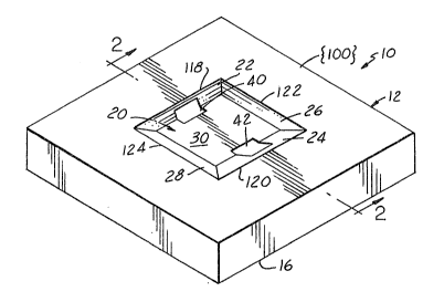
Referring first to Figure 1, aperture
assembly 10 is shown ~or the purposes of illustrating an
example in which the invention is used to advantage.
. .
.
.
~3~
Ap~rture assembly 10 is here shown fabricated ~rom a
~100~ sllicon substrate 12 which has been sawed ~rom a
wafer, by conventional means, such that top planar
surfaGe 14 and bottom planar surface 16 lie
sub6tantially in the ~1003 nominal crystalline plane.
First etchant pit 20 is shown formed through top planar
surfac~ 1~ with side walls 2~, 24, 26, and 28~ and
botto~ wall 30. Side walls 22, 24, 26, and 28 lie in
the ~ intersecting planes which intersect the (100~
nominal plane at an angle ~ of approximately 54.7. As
shown in more detail later herein with particular
ref2rence to Figure 2, aperture 40 and aperture 4~ are
symmetrically positioned in substrate 12.
It is to be unders~ood that although a ~100}
silicon substrate is shown, the invention may be used to
advantage with substrates having major surfaces lying in
other planar directions such as, for example, ~llO}
~ilicon. In general, the invention may be used to
advantage with any monocrystalline subætrate.
Referring now to Figure 2, aperture 40 and
aper~:ure 42 are generally defined by the intersection of
top etchant pit 20 with respeative bottom etchant pit 44
and bot~om etchant pit 4 6 . As described in greater
detail later herein with particular reference to Figures
25 3A through 3C, bottom etchant pit 44 is defined by side
walls 48, 50, 52 (not shown) and 54 (not shown) lying in
tha ~ intersecting planes, and top wall 56 lying in
thQ { 100 ) plane . Side walls 48, 50, 52, and 54 are
~ormed at an angle ~ with respect to bottom planar
~6~2~3
-- 6
surface 16 or the {100} planes in general.
Aperture plane 62 of aperture 42 is ~hown in
Figure 2 as a plane between protruding edges 64 and 66 of
aperture 42O Protruding edge 64 is deined by the
intersection of top etchant pit 20 with top wall 56 of
bottom etchant pit 44. Protruding edge 66 is defined by
the intersection of bottom etchant pit 44 with bottom
wall 30 of top etchant pit 20. Aperture a~is 68 of
aperture 42 is shown perpendicular to aperture plane 62
midway between protruding edges 64 and 66. The angle of
the aperture plane with respect to bottom planar surface
16, or the {100} planes in general, is herein
designated as angle B.
Aperture 40 is shown in Figure 2 as being
symmetrically formed in substrate 12 with respect to
aperture 42. Bottom etchant pit 46 is having top wall 76
lying in ths {100} plane and side walls 78, 80, 82
(not.shown~, and 84 (not shown) lying in the ~111}
planes. Side walls 78, 80, 82 and 84 are etched at an
angle ~ with respect tc bottom planar surface 16 or the
{100} planes in general.
Aperture plane 92 of aperture 40 is defined as a
planar surface between protruding edges 94 and 96 of
aperture 40. Protruding edge 96 is defined by the
intersection of top etchant pit 20 with top wall 76 of
bottom etchant pit 46. Protruding edge 94 is defined by
the intersection of bottom etchant pit 46 with bottom
wall 30 of top etchant pit 20. Aperture a~is 98 of
aperture 40 is shown perpendicular to aperture plane 92
midway between protruding edges 94 and 96. The angle of
aperture plane 92 with respect to top planar surface 14,
or the {100} planes in general, is herein designated
as angle B.
Referring now to Figures 3A through 3C, wherein
like numerals refer to like parts shown in Figures 1
~. ~
,
-- 7 --
and 2, the fabrication of aperture assembly 10 is now
described. The fabrication steps described herein
utilize photolithographic and etching teehniques well
known in the microelectronics industry. Substrate 12 is
illustrated in Figure 3A as a silicon substrate,
preferably having been sawed to a thickness of
approximately 200 to 500 microns with major surfaces
lying substantially in the {100} planes. Top and
bottom silicon oxide layers 102 and 104, respectively,
are grown on substrate 12 using conventional techniques
well known in the semiconductor industry. Layer of
silicon nitride 106 and layer of silicon nitride 108 are
deposited over respective silicon o~ide layers 102 and
104, respectively, using conventional vapor deposition
techniques. Silicon oside layer 102 and silicon nitride
layer 106, together define passivation layer 107.
Similarly, the combination of silicon oxide layer 104 and
silicon nitride layer 108 define passivation layer 109.
With particular reference to Figure 3B,
photo-resist layers 112 and 114 are deposited over
respective passivation layers 107 and 109. Rectangular
etchant pattern 116 is delineated in photo-resist layer
112 by conventional photolithographic techniques.
Rectangular etchant pattern 116 is etched through
passivation layer 107 thereby exposing a corresponding
rectangular portion of top planar surface 14 for etching
top etchant pit 20 in a subsequent etching step. In a
similar manner, bottom rectangular pattern 126 and bottom
rectangular pattern 128 are delineated through bottom
photo-resist layer 114 and passivation layer 109.
Re~erring now to Figure 3C, a wet anisotropic
etchant solution such as aqueous-potassium-hydroxide
solution or ethylene-diamine-pyrocatecol solution, is
applied to top rectangular pattern 116, bottom
rectangular pattern 126, and bottom rectangular pattern
.
.
.
.3
128 to form respecti~2 top etchant pit 20, bot-tom etchant
pit 44 and bottom etchant pit 46. For the {.100}
silicon wafer illustrated herein, the wet etchant acts
against the {100~ planes at a rate appro~imately 100
times greater than against the ~111} planes. The
etchant steps are timed such that top etchant pit 20 is
etched against the {100} planes to a distance dl
before bottom planar surface 16. Stated another way, top
etchant pit 20 is etched to a depth t-dl where t is the
thickness of substrate 12. During the etching of the
planes to a distance of dl, there will be relatively
little etching against the {111} planes.
Accordingly, sidewalls 22, 24, 26 tFigure 1) and 28
(Figure 1), which lie in the {111} planes, are
slightly offset from rectangular patt~rn 116. More
specifically, the intersection of sidewalls 22, 24, 26
and 28 with top planar surface 14 defines, respectively,
left transverse edge 118, right transverse edge 120,
longitudinal edge 122 (Figure 1), and longitudinal edge
124 ~Figure 1) of etchant pit 20, all of which are
slightly offset from rectangular pattern 116.
Both bottom etchant pit 44 and bottom etchant
pit 46 are etched to a depth d2 before top planar
surface 14. That is, bottom etchant pit 44 and bottom
etchant pit 46 are etched to a depth t-d2. With
respect to bottom etchant pit 44, the intersection of
sidewalls 48, 50, 52 (not shown) and 54 (not shown) with
bottom planar surface 16 defines, respectively, left
transverse edge 130, right transverse edge 132,
longitudinal edge 134 (not shown), and longitudinal edge
136 ~not shown), all of which are slightly offset from
rectangular pattern 126. Referring to bottom etchant pit
46, the intersect;on o sidewalls 78, 80, 82 (not shown)
and ~4 (not shown) with bottom planar surface 16 defines,
respectively, left transverse edge 138, right transverse
~3~
edge 140, longitudinal edge 142 (not shown), and
longitudinal edge 144 (not shown), all of which are
slightly offset from rectangular pattern 128.
Top etchant pit 20 and bottom etchant pits 44
and 46 are here shown etched to the same depth tdl=d2)
such that the etchant steps are performed concurrently.
That is, by etching to the same depth, the timing o~ the
etching step is ~bstantially the ~ame thereby enabling
the etching 8tep8 to be performed concurrently.
The trigonometric relationships o~ the various
etching parameters described herein above with respect
to the de~ired or preselected angle of the aperture
plane is now described with reference to Figure 4. For
clarity of illustration, the following description is
with particular reference to aperture 42. Those skilled
in the art, however, will recognize that the
de~cription herein is also applicable to aperture 40,
and is further applicable to other apertures desired by
a designer which are not specifically illustrated
herein. It is to be further noted that the de~cription
hQrein rela~es to a ~100} silicon wafer. The teachings
described, however, are applicable to other
monocrystalline ~ub~trates such as, for example, {110
crystalline structures wherein the ~111) planes
intersect the plane~ at an angle of 90.
A~ previously described herein with re~erence
to Figure 2, aperture plane 62 extends through
protruding edges 64 and 66 forming angle B with respect
to bottom planar sur~ace 16. S~de walls 48 and 50 of
etahant pit 44 lie along the ~111) planes at an angle ~
to the nominal ~100) plane of 54 . 7 . Preselected angle
B is related to the lonyltudinal distance between le~t
transvQr~e edge 130 of bottom etchant pit and the
opposing right transverse edge 120 o~ top etchant pit 20
.2~3642.
a-
~L~, the preselected distance of top etchant pit 20from bottom planar surface.16 (dl), the preselected
distance of bottom etchant pit 44 from top planar surface
14 (d~, the angle between the {111} planes and the
nominal {100} plane (~) and the thickness of
substrate 12 (t) by the following trigonometric relation:
r t - (dl + d2)1
tan 1 aL - ~dl ~ d2)
_ tan ~ _
Thus, it is seen that the preselected angle B may be
changed by the designer by changing any of the parameters
shown in the above equation. The designer is therefore
able to select a desired aperture angle by simply
selecting from: the type of monocrystaline substrate
t~); wafer thickness (t); longitudinal offset of
opposing etchant pits (QL~; and the etchant time or
thickness (dl + d2~.
This concludes the description of the preferred
embodirnent. The reading of it by those skilled in the
art will bring to mind many alterations and modifications
without departing from the spirit and scope of the
inventionO Accordinyly it is intended that the scope of
the invention be limited only by the following claims.
.
: ' . .