Note: Descriptions are shown in the official language in which they were submitted.
7~3
LOW POWER, HIGH NOISE MARGIN LOGIC GATES EMPLOYING
ENHANCEMENT MODE SWITCHING FETS
Field of the Invention
This invention relates to logic gates haviny
relatively low power consumption and relatively high noise
margins. More particularly, this invention relates to low
power, high noise margin logic gates which employ enhancement
mode field effect switching transistors (FETs).
Background of the Invention
A simple logic gate which employs enhancement mode
switching FETs comprises an enhancement mode switching FET
connected in series with a depletion mode load FET between
two voltage supply terminals, an input terminal connected to
the gate of the switching FET and an output terminal
connected between the switching FET and the load FET. This
logic gate operates as an invertor. If additional switching
FETs are connec~ed in parallel with the first switching FET
and a corresponding input terminal is connected to the gate
of each switching FET, a simple NOR gate is obtained.
Circuits made up of such simple logic gates are known as
Direct Coupled FET Logic (DCFL) circuits.
In order to function properly, DCFL logic circuits
must be designed such that the output "logic low" level is
below the threshold voltage of the enhancement mode switching
FETs. While this may be relatively easy to achieve for
silicon FETs which typically have threshold voltages of a few
volts, it is more difficult to achieve for GaAs MESFETs which
typically have threshold voltages which are an order of
magnitude smaller. Moreover, because the threshold voltage
is small, the noise margin of the l'logic low" level is also
small.
The "logic high't level of a DCFL logic gate is
limited by the output current which flows i~to downstream
logic gates. Thus, a DCFL logic gate which is connected to
several downstream logic gates in parallel may have a "logic
high" level which is close to its "logic low" level. In this
~2~
case, noise margin of the "logic high" level will also be
small.
The noise margins of DCFL gates can be improved by
adding a level shifting buffer stage at the output of each
gate. The level shifting buffer stage shifts the output
level lower to improve the noise margin of the "logic low"
level, and buffers the output to reduce the impact of fanout
on the "logic high" level. However, the level shifting
buffer stage significantly increases the power consumption of
the logic gate. Thus, the improved noise margins are
achieved at the expense of a significant power consumption
penalty. Moreover, most known level shifting buffer stages
require a supply voltage which differs from the supply
voltages applied to the switching stage. The requirement for
a third supply voltage complicates the design and incréases
the cost of circuits employing buffered gates.
Summary of the Invention
This invention seeks to provide logic gates which
employ enhancement mode switching FETs and which have noise
margins comparable to those provided by logic gates having
level shifting buffer stages, but which have lower power
consumption than those logic gates having level shifting
buffer stages.
A logic gate according to the invention comprises
an input tPrminal, an output terminal, and first and second
voltage supply terminals; an enhancement mode switching FET
having a gate connected to the input terminal, a source and a
drain; a load device connected between the drain of the
switching FET and the first voltage supply terminal; a
feedback device connected between the source of the switching
FET and the second voltage supply terminal; a two terminal
level shift device connected between the drain of the
switching FET and the output terminal; and an enhancement
mode pulldown FET having a gate connected to the source of
the switching FET, a source connected to the second voltage
33
supply terminal, and a drain connected to the output
terminal.
The load device may be a depletion mode FET having
a drain which is connected to the first voltage supply
terminal, and a gate and source, both of which are connected
to the drain of the switching FET. Alternatively, the load
device may be a linear or nonlinear resistance.
The feedback device may be an enhancement mode FET
having a source which is connected to the second voltage
supply terminal, and a gate and drain, both of which are
connected to the source of the switching FET. Alternatively,
the feedback device may be a depletion mode FET having a
drain which is connected to the source of the switching FET,
a source, which is connected to the second voltage supply
terminal, and a gate which is connected to either the source
or the drain. The feedback device may also be a diode, a
plurality of diodes connected in series, or a linear or
nonlinear resistance.
The two terminal level shift device may be a diode
or a plurality of diodes connected in series. Alternatively,
the two terminal level shift device may be a linear or
nonlinear resistance, or may be an enhancement mode FET with
its gate and drain connected to the drain of the switching
FET and its source connected to the output terminal.
The logic gate as defined above operates as an
invertor. The logic gate may further comprise one or more
additional enhancement mode switching FETs, each having a
drain connected to the load device, a source connected to the
feedback device, and a gate connected to a corresponding
input terminal. With the additional switching FETs and input
terminals, the logic gate functions as a NOR gate.
The two terminal level shift device of the logic
gate according to the invention shifts the output "logic low'~
level down while the feedback device effectively shifts the
threshold voltage of the switching FET to a level which is
further from the supply voltage at the second voltage supply
terminal to ensure that the "logic low" level is well below
the effective threshold voltage of the switching FETs of
3~
downstream gates. Moreover, the feedback device also shifts
the output "logic high" level higher by increasing the
effective input impedance of downstream gates. Thus the
logic gate according to the invention has better noise
margins than DCFL gates.
Moreover, because the load current is split between
the switching FET and the pulldown FET when the switching FET
is on, the switching FET can be made narrower than in DCFL
and buffered gates to reduce the power consumption by an
amount which is greater than the power consumption of the
level shift device, feedback device and pulldown FET. Hence,
the logic gate according to the invention provides good noise
margins with relatively low power consumption.
Furthermore, the logic gate according to the
invention requires only two voltage supply levels in contrast
to some high noise margin buffered gate designs which require
three voltage supply levels.
Brief Description of the ~rawings
Embodiments of the invention are described below by
way of example only with reference to the accompanying
drawings, in which:
Figure 1 is a schematic diagram of a direct coupled
FET invertor:
Figure 2 is a schematic diagram of a buffered FET
invertor;
Figure 3 is a schematic diagram of an invertor
according to a first embodiment;
Figure 4 is a schematic diagram of an invertor
according to a second embodiment;
Figure 5 is a schematic diagram o~ an invertor
according to a third embodiment;
Figure 6 is a schematic diagram of an invertor
according to a fourth embodiment; and
Figure 7 is a schematic diagram of a NOR gate
according to a fifth embodiment.
~8~;733
Detailed Description of Embodiments
Figure 1 is a schematic diagram of a direct coupled
FET invertor lo. The invertor lo comprises an input terminal
12, an output terminal 14, a firsk voltage supply terminal 16
for connection to a positive supply voltage VDD, and a second
voltage supply terminal 18 for connection to ground. The
invertor 10 further comprises an enhancement mode switching
FET 20 having a gate 22 connected to the input terminal 12,
a source 24 connected to the second voltage supply terminal
18, and a drain 26 connected to the output terminal 14. The
invertor 10 also comprises a depletion mode load FET 30
having a drain 32 connected to the first voltage supply
terminal 16, and a gate 34 and source 36 connected to the
drain 26 of the switching FET 20.
When a voltage which is less than the threshold
voltage of the switching FET 20 is applied to the input
terminal 12 of the invertor 10, the switching FET 20 is off
and the load FET 30, which is always on, pulls the voltage of
the output terminal 14 to a "logic high" level. The "logic
high" level is limited by the positive supply voltage VDD and
by the effective input impedance of downstream gates which,
together with the load FET 30 act as a voltage divider to
determine the "logic high" level. If the positive supply
voltage VDD is low or the effective input impedance of
downstream gates is s ~ relatively small (as will be the
case when several gates are connected in parallel to the
output terminal 14 of the invertor 10), the "logic high"
level will be close to the threshold voltage of the switching
FETs 20 of downstream gatesl and the "logic high" level will
have a small noise margin.
When a voltage which exceeds the threshold voltage
of the switching FET 20 is applied to the input terminal 12,
the switching FET 20 turns on, and the switching FET 20 and
the load FET 30 act as a voltage divider to determine the
voltage on the output terminal 14. I'he resulting output
voltage is a "logic low" for succeeding stages only if it is
less than the threshold voltage of the switching FET 20.
~L2~;7~3
Where the switching FET 20 is a GaAs MESFET, the
threshold voltage is approximately 0.25 volt. Thus, for a
typical supply voltage of VDD=2.5V, the on-state impedance of
the switching FET 20 must be made less than one tenth the on-
state impedance of the load FET 30. This is typicallyaccomplished by making the channel of the switchiny FET 20
approximately three times wider than the channel of the load
FET 30 and by arranging for the "logic high" level to exceed
the threshold voltage of the switching FET 20 by an amount
sufficient to ensure that a "logic high" input turns the
switching FET 20 fully on. This places constraints on the
"logic high" level which further limit the noise margin of
that level. Moreover, because the resulting "logic low"
voltage level is very close to the threshold voltage of the
switching FET 20, the noise margin of the "logic low" is also
very small when GaAs MESFETs 20, 30 are used.
Figure 2 is a schematic diagram of a buffered FET
invertor which comprises the invertor 10 described above, and
a level shifting buffer stage 50 connected to the output
terminal 14 of the invertor 10. The level shifting buffer
stage 50 comprises an enhancement mode FET 60 having a gate
62 which is connected to the output terminal 14 of the
invertor 10, a drain 64 which is connected to the positive
voltage supply terminal 16 and a source 66 which is connected
to a buffer stage output terminal 70. The level shifting
buffer stage further comprises a depletion mode FET 80 which
has a drain 82 which is connected to the buffer stage output
terminal 70, and a gate 84 and source 86 which are both
connected to a negative voltage supply terminal 90 for
connection to a negative supply voltage Vss
When a voltage which is less than the threshold
voltage of the switching FET 20 is applied to the input
terminal 12 of the invertor 10, the switching FET 20 is off
and the load FET 30, which is always on, pulls the voltaye of
3S node 14 to a level close to the positive supply voltage VDD.
This causes FET 60 to turn on, and FETs 60, 80 of the buffer
stage and the effective input impedance of downstream gates
act as a voltage divider to determine the voltage on the
33
output terminal 70. The channel of EET ~0 is made wider than
the channel of FET 80 to ensure that the voltage on the
output terminal 70 is considerably larger than the threshold
voltage of the switching FET 20 wh~n a voltage less than the
threshold voltage of the switching FET 20 is applied to the
input terminal 12, even when the effective input impedance of
downstream gates is relatively low. This ensures that the
voltage on the output terminal 70 will act as a "logic high"
for succeeding logic gates which employ switching FETs
similar to the FET 20, and that the noise margins for this
state will be acceptably large.
When a voltage which exceeds the threshold voltage
of the switching FET 20 is applied to the input ter~.inal 12,
the switching FET 20 turns on, and the switching FET 20 and
the load FET 30 act as a voltage divider to determine the
voltage on the node 14. If the voltage on the node 14 is low
enough, the FET 60 turns off and the FET 80, which is always
on, pulls the voltage on the output terminal 70 toward the
negative supply voltage Vss. The resulting output voltage is
considerably lower than the threshold voltage of the
switching FET 20 and will act as a "logic low" for succeeding
logic gates which employ switching FETs similar to the FET
20. Indeed, the "logic low" level can be below ground so
that the noise margin for this state is acceptably large in
spite of the low threshold voltage of the switching FET 20.
Unfortunately, in the buffered invertor shown in
Figure 2, the switching FET 20 must still be made wider than
the load FET 30 in order to ensure that the voltage on the
node 14 when the switching FET 20 is on is low enough to turn
off the FET 60 of the buffer stage 50. In particular, the
FET 20 must be made roughly twice as wide as the load FET 30.
As the minimum dimensions of the load FET 30 are determined
by processing considerations, a large switching FET 20 is
required. Moreover, the level shifting buffer stage~ 50
increases the power consumption of the buffer~d invertor.
Thus, the addition of the level shifting buffer stage 50
improves the noise margins and drive capability of the
invertor 10, but significantly increases the power
consumption of the resulting buffered invertor. The power
consumption of the buffered invertor is approximately 1.0 mW
when implemented in 1 micron GaAs MESFET technology with a
minimum transistor width of 3 microns.
The buffered invertor also requires three voltage
supply levels in contrast to the two voltage supply levels
required by the direct coupled FET invertor 10 shown in
Figure 1. This complicates the design and increases the cost
of circuits using the buffered FET invertor.
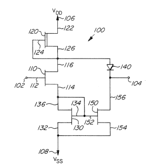
Figure 3 is a schematic diagram of a logic gate
according to a first embodiment in the form of an invertor
100. The invertor 100 comprises an input terminal 102, an
output terminal 104, a first voltage supply ter~inal 106 for
connection to a positive voltage supply VDD, and a second
voltage supply terminal 108 for connection to a negative
voltage supply Vss. The invertor 100 further comprises an
enhancement mode switching FET in the form of a GaAs MESFET
110 having a gate 112 which is connected to the input
terminal 102, a source 114 and a drain 116. A load device of
20 the invertor 100 comprises~a depletion mode GaAs MESFET 120
having a drain 122 which is connected to the first voltage
supply terminal 106, and a gate 124 and a source 126, both of
which are connected to the drain 116 of the switching FET
110. A feedback device of the invertor 100 comprises an
2S enhancement mode GaAs MESFET 130 having a source 132 which is
connected to the second voltage supply terminal 108 and a
gate 134 and drain 136, both of which are connected to the
source 114 of the switching FET 110. A two ter~inal level
shift device of the invertor 100 comprises a diode 140
30 connected between the drain 116 of the switching FET 110 and
the output terminal 104. The invertor 100 further comprises
an enhancement mode pulldown GaAs ~ESFET 150 having a gate
152 which is connected to the source 114 of the switching FET
110, a source 154 which is connected to the second voltage
35 supply terminal 108, and a drain 156 which is connected to
the output terminal 104.
When a "logic low" voltage i5 applied to the input
terminal 102, the switching FET 110 is off, so the feedback
7~
FET 130 and the pulldown FET 150 are also off. The load FET
120, which is always on, together with the diode 140 and the
effective input impedance of downstream gates act as a
voltage divider to determine the voltage on the output
terminal 104. However, the feedback and pulldown FETs
130,150 of the downstream gates increase the effective input
impedance of the downstream gates to a value which is higher
than the effective input impedance of DCFL gates such as the
invertor 10 which lack these components. Consequently, the
output "logic high" level for the invertor 100 is hiqher than
the output "logic high" level for the DCFL invertor 10 when
each is connected to an equivalent complement of similar
downstream gates. As a result, the noise margin for the
"logic high" level of the invertor 100 is larger than the
noise margin for the "logic high" level of the DCFL invertor
10 .
When a "logic high" level is applied to the input
terminal 102, the switching FET 110 turns on, thereb~ turning
on the feedback FET 130 and the pulldown FET 150. The load
FET 120 and the switching FET 110, feedback FET 130, diode
140, and pulldown FET 150 act as a voltage divider to
determine the voltage on the drain 116 of the switching FET
110. The diode 140 and the pulldown FET 150 act as a voltage
divider which fixes the voltage on the output terminal 104 at
a "logic low" level. The pulldown FET 150 pulls the voltage
on the output terminal 104 toward the negative supply voltage
VsS, and the diode 140 provides the required voltage shift
between the drain 116 of the switching FET 110 and the output
terminal 104. If a greater voltage shift between the drain
116 of the switching FET 110 and the output terminal 104 is
desired for improved noise margins, the diode 140 can be
replaced by a plurality of series connected diodes.
Because the current drawn by the load FET 120 is
divided between the switching FET 110 in series with the
feedback FET 130 and the diode 140 in series with the
pulldown FET 150, and because of the level shifting effect of
the diode 140, an acceptably low "logic low" output voltage
can be achieved even when all of the FETs 110, 120, 130, 150
have substantially the same channel width. Hence all of the
FETs can be made as small as the fa~rication technoloyy will
permit. Consequently, the power consumption of the resultiny
invertor 100 is substantially lower than that of the buffered
5 FET invertor shown in Figure 2. The power consumption of the
invertor 100 is approximately 0.25 mW when implemented in 1
micron GaAs MESFET technology using minimum transistor widths
of 3 microns, significantly lower than the power consumption
OI the buffered FET invertor shown in Figure 2 when
10 implemented in the same technology.
Moreover, the level shifting diode 1~0 shifts the
output "logic low" level down and the feedback and pulldown
FETs 130, 150 shift the input "logic high" level up to
increase the voltage swing and hence the available noise
15 margins of the invertor 100. Indeed, the logic levels and
noise margins of the invertor 100 can be made compatible with
the logic levels and noise margins of the buffered FET
invertor shown in Figure 2, so that the devices can be
combined in a common circuit. The invertor 100 can be used
20 where output drive is not important to reduce power
consumption, and the buffered invertor of Figure 2 can be
used to provide greater output drive where required at the
expense of higher power consumption.
The invertor 100 also requires only positive and
25 neqative supply voltages VDD and Vss. The elimination of the
ground connection required for the buffered FET invertor of
Figure 2 simplifies the design of circuits using the invertor
100 .
Figure 4 is a schematic diagram of a logic gate
30 according to a second embodiment in the form of an invertor
200. The invertor 200 comprises an input terminal 202, an
output terminal 204, a first voltage supply terminal 206 for
connection to a positive voltage supply VDD, and a second
voltage supply terminal 208 for connection to a negative
35 voltage supply Vss. The invertor 200 further comprises an
enhancement mode switching FET in the form of a GaAs MESFET
210 having a gate 212 which is connected to the input
terminal 202, a source 214 and a drain 216. A load device of
'733
11
the invertor 200 comprises a resistor 220 which is connected
between the first voltage supply terminal 206 and the drain
216 of the switching FET 210. A feedback device of the
invertor 200 comprises another resistor 230 which is
connected between the second voltage supply terminal 208 and
the source 214 of the switching FET 210. A two terminal
level shift device of the invertor 200 comprises another
resistor 240 connected between the drain 216 of th~ switching
FET 210 and the output terminal 204. The invertor 200
further comprises an enhancement mode pulldown GaAs MESFET
250 having a gate 252 which is connected to the source 214 of
the switching FET 210, a source 254 which is connected to the
second voltage supply terminal 208, and a drain 256 which is
connected to the output terminal 204.
When a "logic low" voltage is applied to the input
terminal 202, the switching FET 210 is of~, so no current
flows through the feedback resistor 230 and the pulldown FET
250 is also off. The load FET 220, which is always on,
together with the level shift resistor 240 and the effective
input impedance of downstream gates act as a voltage divider
to determine the voltage on the output terminal 204.
H~wever, the feedback resistor 230 and the pulldown FET 250
of the downstream gates increase the effective input
impedance of the downstream gates to a value which is higher
than the effective input impedance of DCFL gates such as the
invertor 10 which lack these components. Consequently, the
output "logic high" level for the invertor 200 is higher than
the output "logic high" level for the DCFL invertor 10 when
each is conn~cted to an equivalent complement of similar
downstream gates. As a result, the noise margin for the
"logic high" level of the invertor 200 is larger than the
noise margin for the 'llogic high" level of the DCFL invertor
10 .
When a "logic high" level is applied to the input
terminal 202, the switching FET 210 turns on, thereby
supplying enough current to feedback resistor 230 to turn on
the pulldown FET 250. The load resistor 220 and the
switching FET 210, feedback resistor 230, level shift
73;~
12
resistor 240, and pulldown FET 250 act as a voltage divider
to determine the voltage on the drain 216 of the switching
FET 210. The level shift resistor 240 and the pulldown FET
250 act as a voltage divider which fixes the voltage on the
output terminal 204 at a "logic low" level. The pulldo~m FET
250 pulls the voltage on the output terminal 204 toward the
negativP supply voltage Vss, and the level shift resistor 240
provides the required voltage shift between the drain 216 of
the switching FET 210 znd the output terminal 204. If a
greater voltage shift between the drain 216 of the switching
FET 210 and the output terminal 204 is desired for improved
noise margins, the resistance of the level shift resistor 204
can be increased.
Because the current drawn by the load FET 220 is
divided between the switching FET 210 in series with the
feedback resistor 230 and the level shift resistor 240 in
s~ries with the pulldown FET 250, and because of the level
shifting effect of the resistor 240, an acceptably low "logic
low" output voltage can be achieved even when the switching
FET 210 is made with the minimum channel width which
fabrication technology will permit. Consequently, the power
consumption of the resulting invertor 200 can be made
substantially lower than that of the buffered FET invertor
shown in Figure 2. Moreover, the level shifting resistor 240
shifts the output "logic low" level down and the feedback
resistor 230 and the pulldown FET 250 shift the input "logic
high" level up to increase the voltage swing and hence the
available noise margins of the invertor 200. The invertor
200 also requires only positive and negative supply voltages
VDD and Vss. Any or all of the resistors 220, 230, 240 may
be non-linear resistors.
Figure 5 is a schematic diagram of a logic gate
according to a third embodiment in the form of an invertor
300. The invertor 300 comprises an input terminal 302, an
output terminal 304, a first voltage supply terminal 306 for
connection to a positive voltage supply VDD, and a second
voltage supply terminal 308 for connection to a negative
voltage supply Vss. The invertor 300 further comprises an
33
enhancement mode switching FET in the form of a GaAs MESFET
310 having a gate 312 which is connecte~ to the input
terminal 302, a source 314 and a drain 316. A load device of
the invertor 300 comprises a depletion mode ~aAs MESFET 320
having a drain 322 which is connected to the firsk voltage
supply terminal 306, and a gate 324 and a source 326, both of
which are connected to the drain 316 of the switching FET
310. A feedback device of the invertor 300 comprises a diode
330 which is connected between the second voltage supply
terminal 208 and the source 314 of the switching FET 310. A
two terminal level shift device of the invertor 300 comprises
an enhancement mode GaAs MESFET 340 having a gate 342 and a
drain 344 which are connected to the drain 316 of the
switching FET 310 and a source 346 which is connected to the
output terminal 304. The invertor 300 further comprises an
enhancement mode pulldown GaAs MESFET 350 having a gate 352
which is connected to the source 314 of the switching FET
310, a source 354 which is connected to the second voltage
supply terminal 308, and a drain 356 which is connected to
the output terminal 304.When a "logic low" voltage is applied
to the input terminal 302, the switching FET 310 is off, so
no current flows through the feedback diode 330 and the
pulldown FET 350 is also off. The load FET 320, which is
a'ways on, together with the level shift FET 340 and the
effective input impedance of downstream gates act as a
voltage divider to determine the voltage on the output
terminal 304. However, the feedback diode 330 and the
pulldown FET 350 of the downstream gates increase the
effective input impedance of the downstre~m gates to a value
which is higher than the effective input impedance of DCFL
gates such as the invertor 10 which lack these components.
Consequently, the output "logic high" level for the invertor
300 is higher than the output "logic high" level for the DCFL
invertor 10 when each is connected to an equivalent
complement of similar downstream gates. As a result, the
noise margin for the "logic high" level of the invertor 300
is larger than the noise margin for the "logic high" level of
the DCFL invertor lO.
~21~73;~
14
When a "logic high" level is applied to the input
terminal 302, the switching FET 310 turns 021, thereby
supplying enough current to feedback diode 330 to turn on the
pulldown FET 350. The load FET 320 and the switching FET
310, feedback diode 330, level shift FET 340, and pulldown
FET 350 act as a voltage divider to determine the voltage on
the drain 316 of the switching FET 310. The level shift FET
340 and the pulldown FET 350 act as a voltage divider which
fixes the voltage on the output terminal 304 at a ~710gic low"
level. The pulldown FET 350 pulls the voltage on the output
terminal 304 toward the negative supply voltage Vss, and the
level shift FET 340 provides the required voltage shift
between the drain 316 of the switching FET 310 and the output
terminal 304.
Because the current drawn by the load FET 320 is
divided between the switching FET 310 in series with the
feedback diode 330 and the level shift FET 340 in series with
the pulldown FET 350, and because of the level shifting
effect of the FET 340, an acceptably low "logic low" output
voltage can be achieved even when the switching FET 310 is
made with the minimum channel width which fabrication
technology will permit. Consequently, the power consumption
of the resulting invertor 300 can be made substantially lower
than that of the buffered F~T invertor shown in Figure 2.
Moreover, the level shifting FET 340 shifts the output "logic
low" level down and the feedback diode 330 and the pulldown
FET 350 shift the input '~logic high" level up to increase the
voltage swing and hence the available noise mar~ins of the
invertor 300. The invertor 300 also requires only positive
and negative supply voltages VDD and Vss. The feedback diode
330 may be replaced with a plurality of series connected
diodes if required to ensure turn-on of the pulldown FET 350
when the switching FET 310 turns on.
Figure 6 is a schematic diagram of a logic gate
according to a rourth embodiment in the form of an invertor
400. The invertor 400 comprises an input terminal 402, an
output terminal 404, a first voltage supply terminal 406 for
connection to a positive voltage supply VDD, and a second
voltage supply ~erminal 408 for connection to a negative
voltage supply Vss. The invertor 400 further comprises an
enhancement mode switching FET in the form of a GaAs MESFET
410 having a gate 412 wh.ich is connected to the input
terminal 402, a source 414 and a drain 416. A load device o~
the invertor 400 comprises a depletion mode GaAs MESFET 420
having a drain 422 which is connected to the first voltage
supply terminal ~06, and a gate 424 and a source 426, both of
which are connected to the drain 416 of the switching FET
410. A feedback device of the invertor 400 comprises a
depletion mode GaAs MESFET 430 having a source 432 and a gate
434 which are both connected to the second voltage supply
terminal 408, and a drain 436 which is connected to the
source 414 of the switching FET 410. A two terminal level
shift device of the invertor 400 comprises a diode 440
connected between the drain 416 of the switching FET 410 and
the output terminal 404. The invertor 400 further comprises
an enhancement mode pulldown GaAs MESFET 450 having a gate
452 which is connected to the source 414 of the switching FET
410, a source 454 which is connected to the second voltage
supply terminal 408, and a drain 456 which is connected to
the output terminal 404.
The invertor 400 operates in essentially the same
manner as the invertor 100 shown in Figure 3, except that the
feedback device is a depletion mode FET 430 which pulls the
gate 452 of the pulldown FET 450 toward Vss when the
switching FET 410 is off to turn off the pulldown FET 450 and
which provides a voltage drop sufficient to turn the pulldown
FET 450 on when the switching FET 410 is on.
In the invertor 400, the gate 434 of the depletion
mode feedback FET may be connected to its drain 436 instead
of its source 432.
. Figure 7 is a schematic diagram of a logic gate
according to a first embodiment in the form of a NOR gate
35 500. The NOR gate 500 comprises three input terminals 502a-
c, an output terminal 504, a first voltage supply terminal
506 for connection to a positive voltage supply VDD, and a
second voltage supply terminal 508 for connection to a
'733
16
negative voltage supply Vss. The NOR gate 500 further
comprises three enhancement mode switchir.g FETs in the form
of GaAs MESFETs 510a-c, each having a gate 512 which is
connected to a corresponding one of the input terminals 502a-
c, a source 514 connected to the sources 514 of each of the
other switching FETs, and a drain 516 connected to the drains
516 of each of the other switching FETs. A load device of
the NOR gate 500 comprises a depletion mode GaAs MESFET 520
having a drain 522 which is connected to the first voltage
supply terminal 506, and a gate 524 and a source 526, both of
which are connected to the drains 516 of the switching FETs
510a-c. A feedback device of the NOR gate 500 comprises an
enhancement mode ~aAs MESFET 530 having a source 532 which is
connected to the second voltage supply terminal 508 and a
gate 534 and drain 536, both of which are connected to the
sources 514a-c of the switching FETs 510a-c. A two terminal
level shift device of the NOR gate 500 comprises a diode 540
connected between the drains 516a-c of the switching FETs
510a-c and the output terminal 504. The NOR gate 500 further
comprises an enhancement mode pulldown GaAs MESFET 550 having
a gate 552 which is connected to the sources 514a-c of the
switching FETs 510a-c, a source 554 which is connected to
the second voltage supply terminal 508, and a drain 556 which
is connected to the output terminal 504.
The NOR gate 500 is essentially the same as the
invertor 100 shown in Figure 3 except that three input
terminals 502a-c and three switching FETs 510a-c are
provided. When a "logic low" voltage is applied to all input
terminals 502a-c, all switching FETs 510a-c are o~f, so the
feedback FET 530 and the pu]ldown FET 550 are also off. The
load FET 520, which is always on, pulls the drains 516a-c of
the switching FETs 510a-c toward VDD, so that the output
terminal 504 is also pulled to a "logic high" level close to
VDD. When a "logic high" level is applied to one or more of
the input terminals 502a-c, the corresponding switching FET
or FETs 510 turn on, thereby turning on the feedback FET 530
and the pulldown FET 550. The load FET 520 and the switching
FET or FETs 510 which are turned on, feedback FET 530, diode
17
540, and pulldown FET 550 act as a voltage divider to
determine the voltage on the drains 516a-c of the switching
FETs 510a-c. The diode 540 and the pulldown FET 550 act as a
voltage divider which fixes the voltage on the output
5 terminal 504 at a "logic low" level. The pulldown FET 550
pulls the voltage on the output terminal 504 toward the
negative supply voltage V~s, and the diode 540 provides the
required voltage shift between the drains 516a-c of the
switching FETs 510a-c and the output terminal 504. If a
greater voltage shift between the drains 516a-c of the
switching FETs 510a-c and the output terminal 504 is desired
for improved noise margins, the diode 540 can be replaced by
a plurality of series connected diodes.
In the invertor 100 and particularly in the NOR
15 gate 500 the feedback FET 130, 530 reduces the temperature
sensitivity of the operating characteristics. A temperature
shift which increases the source current of the switching
FETs 110, 510a-c increases the voltage across the feedback
FET 130, 530 to reduce the gate to source voltage of the
20 switching FETs 110, 510a-c. A temperature shift which
decreases the source current of the switching FETs 110, 510a-
c decreases the voltage across the feedback FET 130, 530 to
increase the gate to source voltage of the switching FETs
110, 510a-c. Hence the feedback FET 130, 530 provides a
measure of temperature compensation.
While the invention has been described in terms of
embodiments employing GaAs MESFETs and is particularly useful
when these devices are employed, other types of FETs may be
employed. For example, Si or InP MESFETs, or JFETs, HEMTs,
HIGFETs or SISFETs may be used.
The invention, which is not limited to the
embodiments described above, is defined by the claims which
follow.