Note: Descriptions are shown in the official language in which they were submitted.
C-3951
F 1256
ELECTROOPTICAL DEVICE
Field Or the Inventlon
This invention relates to an electrooptical
device and more particularly to such a device whose
light transmittance or reflecting characteristics may
be controlled by an applied electrical field. Such a
device is often termed an electrochromic device.
Background of the_Invention
Electrochromic devices are of increasing
importance particularly in the automotive industry and
the invention will be described for specific use in
such industry although a wider use clearly is apparent.
In the automotive industry, electrochromic
devices would be use~ul in the glass portions of an
automotive vehicle. More particularly, an
electrochromic windshield would be useful so that the
transmission o~ light into the passenger compartment
could be regulated to facilitate the heat management of
such compartment. For example, it is advantageous to
control the transmittance o~ infrared and visible
radiatlon ~rom the sun into the passenger compartment
during the heat o~ the day to reduce the load on the
air conditioning requirement. Similarly, it would be
desirable to reduce the transmittance of vlsible light
through the slde wlndows of an automobile to permit
privacy to its interlor when deslred. Aq a
con~equence, the automotive industry i8 showing
considerable lntere~t in so-called "smart wlndows"
through whlch llght transmittance can be controlled
~k
3676~
either manually or automatically.
Additionally, there also are electrochromic
appllcatlons~ such as for a rear-vlew mlrror of an
automotlve vehlcle, in which it would be deslrable to
change its reflectance automatlcally in response to
photoelectrlc sensing of approachlng headlights, to
reduce the glare on the driver of the vehicle.
Electrochromic devices typically involve a
rlgid passive substrate that provides structural
support, such as a layer of glass, for the active
portlon whlch comprlses a multilayer sandwlch of
elements. Generally, the two outer layers of the
active portion serve as the two terminal electrodes for
the electronic current of the device. Between these
terminal electrodes are sandwiched an electrochemical
cell which generally comprises in succession a layer of
an electrochromic material, a layer of an electrolyte,
either solld or liquld, and a counter electrode. When
a dc voltage ls applied across the two terminal
electrodes, electrons are elther ln~ected ln or e~ected
out of the electrochromlc layer at lts interface with
the terminal electrode whlle sultable ions are in~ected
lnto or eJected from the electrochromlc layer at lts
electrolyte lnterface. The electrolyte must conduct
the ions participatlng ln the electrochemlcal reaction
that cau~es the color change. The counter electrode
must be reversible to the saMe ions slnce it must allow
the color changlng reaction to proceed ln the rever~e
dlrection so that the electrochromlc layer may be also
uncolored or "bleached" when deslred. The counter
7~
electrode may also store the lons involved ln the
coloratlon reaction. In some lnstance~, khe counter
electrode may also serve as one of the two terminal
electrodes. For most applicatlons, the electrolyte,
the counter electrode and the two terminal electrodes
need to be transparent.
The depth of color change and the resulting
transmittance change in the electrochromic layer depend
on the amount of ionic charge in~ected into or eJected
~rom the electrochromic layer. In one sense, an
electrochromic cell is basically a battery with a
visible state of charge.
A wide variety of materials are known to be
useful for coloring in the manner described and include
some which can be colored cathodically in an
electrochemical cell, such as tungstic oxide (W03) and
molybdenum oxide (MoO3), and others which can be
colored anodically in an electrochemical cell, such as
iridium oxide.
Similarly~ a wide range of materials have
been proposed, both liquid and solid, for use as the
electrolyte. Superionic conductors and polymeric ion
conductors are available ln solid form.
Typically, the terminal electrodes are of
transparent tin oxide doped to be highly conductlve.
When an electrochromic device of the kind
descrlbed has been used as the window o~ an automobile,
the wlndow is o~ten subJect to non-uniform coloratlon
(darkening) and bleaching (lightenlng) as its
transmission is varied. Such non-uniformlty is
~367~
undesirable and the present invention provides a
solution to thls problem.
Summary of the Invention
I have found that this nonuniformity in many
cases results from the nonunlformity ln the effective
potential actlng on the electrochemical cell. In
partlcular, the effective potential has a lateral
variation because of the voltage drop resulting from
the lateral resistance of the terminal electrodes. The
present invention i8 based on making more uniform the
potential acting on the electrochemical cell.
To this end, in accordance with the present
invention, there i8 included in the electronic part of
the circuit between the two terminal electrode layers
an auxiliary electronically conducting layer of
a material such that the resistance normal to the
surface of this layer effectively dominates the lateral
variation in the resistance of the terminal electrode
layers. This normal resistance may either result from
the resistance of the material in the bulk of the
auxillary layer or may result from the contact
resistance introduced by the barrler between the
auxiliary layer and the contlguous termlnal electrode
layer. As a result of the inclusion of this auxiliary
electrode layer, the potential over the entire surface
of the electrochemical cell is made more unlform
because the degree of lateral variation of the voltage
drop in the termlnal electrode layer ls reduced. The
resistivity of this layer however should not be so hlgh
3 that excessively high voltages need to be applied to
~86~
the terminal electrodes to achieve the electrochromic
ePfect.
Brief Description of the Drawin~s
The invention will be be~ter understood from
the Pollowing more detailed descriptlon t,aken ln
conJunctlon with the accompanylng drawings in whlch:
FIG. 1 lllustrates schematlcally a
cross-section of an electrochromlc devlce typical of
the prior art;
lo FIG. 2 shows schematically a dlagram of the
equivalent resistance circuit of the device of FIG. l;
FIG. 3 illustrates in the manner of FIG. 1 an
electrochromic device in accordance with an embodiment
oP the invention; and
FIGL 4 similarly shows schematically the
equivalent resistance circult of the embodiment of FIG.
4.
Detailed Descriptlon
A prior art electrochromlc device 10 shown in
FIG. 1 includes the planar glass substrate 11 which
provides structural support and ruggedness to the
device but is otherwise passive. Supported on this
substrate ls a stack oP coatings or layers 12 through
16, oP which layer~ 12 and 16 are the termlnal
electrode layers. Across these terminal layers, there
ls establi~hed a voltage supplied by a dc source 19
which may be varied, either manually or electronically.
Generally, these terminal layers are oP tin oxlde
(SnO2) doped to increase its electrical conductivity.
Such layers can be highly light-transmissive. A
7~2
typical thickness for each of these layers is about 100
nanometers b
The lntermedlate layers 13, 14 and 15
basically form a spectroelectrochemlcal cell or
thin-fllm batt~ry whose color is dependent on its state
of charge; to color or to bleach the cell requires only
the char~e or dlscharge of its electrochromic film. In
this cell, layer 13 is of the electrochromic material,
layer 14 is of an ionic conductor and layer 15 is the
counter electrode, that may also be electrochromic.
For example, layer 13 may be o~ hydrous nlckel oxide
Ni(OH)2.xH20 and of a thickness of about 50 nanometers.
The layer 15 that serves as the counter electrode
typically may be a layer o~ a materlal such as
manganese hydroxide whlch is both an ionic and an
electronlc conductor, of thickness comparable to that
of layer 15. The electrolytlc layer 14 may be o~ lM
potassium hydroxide, typlcally 100 micrometers thick.
The coloration reactlon ln a gross sense 18
similar to the anodlc charging reaction in nickel oxide
battery electrodes where dlvalent nickel oxide is
oxidized to rorm a more colored trivalent nickel oxlde.
Bleachlng occurs when the reactlon is reversed. The
change ln coloration tends to be contlnuous with change
ln the potentlal of the cell.
FIG. 2 1~ an equivalent circult schematlc
whlch lllustrates the resistance experlenced in the
terminal electrode layer 12 to reach lts electric
contact 12A by the electron current (as dlstlngulshed
~rom the lonlc current in the cell portion) that is
associated wlth the paths of three different llght
rays, A~ B and C shown ln FIG. 1. Each is through
regions of the termlnal electrode layer 12 su~ces31vely
further dlsplaced by a unit length from the edge of the
layer 12 where the voltage is being applied, The
resistance R in FIG. 2 is the resistance per unit
length in the lateral direction parallel to the plane
of the layer, A s~mllar situation exists at the other
terminal electrode 16. It is evident that at node 21,
corresponding to the Polnt of entry of ray A into layer
12, the voltage drop from the electrical contact 12A,
will be less than at nodes 22 and 23~ corresponding to
the points of entry of rays B and C lnto layer 12. This
means that the voltage at node 21 wlll be higher than
at nodes 22 and 23 so that the electrochemlcal cell
formed by layer 13~ 14 and 15 wlll experience a higher
applied potential at the point corresponding to node 21
than it will at points corresponding to nodes 22 and
23, resulting in a different amount of colorizatlon at
the point corresponding to node 21. Similar
considerations result in a different degree Or coloring
at the point corresponding to node 22 than at the point
corresponding to the node 23. If a low resi~tance
metal layer is deposited over all the edges of the
terminal layer 12 for use as the connection to a lead
from the voltage supply, electrlcal contact 12A
essentially corresponds to the edge nearest the point
being considered.
One solution to this problem would be to
3 increase the lateral conductivlty of the layer 12, as
7~i~
could be done by increasing the thickness of the layer,
since its conductlvity wlll increase with thickne3s.
However a trade of~ with the transparency of this layer
eventually needs to be made. With material~ presently
available ~or use as the layer 12, a limit in thickness
for adequate transparency ls reached before thl~
non-uniformity problem ls solved for electrochromic
wlndows of siæe needed for automobile use.
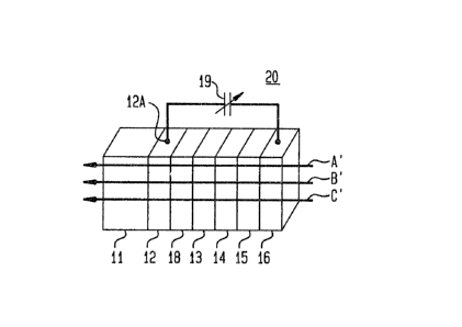
Referring now to ~IG. 3, there is shown an
lo electrochromic device 20 ln accordance with the present
invention. Device 20 lessens the dependence of the
effective potential on a particular point of the
electrochromic layer 13 on its distance from the
electrical contact 12A of the layer 12 where the full
voltage is being applied, through the use of an added
transparent auxiliary layer 18 between the terminal
layer 12 and the electrochromic layer 13. The
reference numerals used in FIG. 1 are carried over to
FIG. 3 for corresponding elements~
This auxiliary layer 18 is chosen to have a
resistance in the direction normal to the plane of the
layer which is high relative to its resistance in the
plane of the layer. The equivalent schematic circuit
for electrons along paths in the terminal electrode
layer 12 and auxiliary layer 18 corresponding to light
rays A, B and C ls depicted in FIG. 4 ln the manner
described in connectlon wlth FIG. 2. In this case, the
resistance normal to the surface per unlt area through
thls auxiliary layer 18 ls R'. If the value R' is
sufficlently higher than R, it is evldent from the
6~6~
equivalent circuit depicted, that the percentage
variatlon in total series resistance from either of the
nodes 31, 32 and 33 to node 34 will be less than the
percentage variation in series resistance from either
of nodes 21, 22 and 23 to node 24. In particular, if
R' is much larger, for example by a factor of ten, than
R, the reslstance in each of the three paths depicted
in FIG. 4 will remain approximately equal to R' whereas
for the three paths depicted in FIG. 2, the resistances
will be R, 2R and 3R, respectively.
It can be appreciated that the R' resistance
will be the sum both of the bulk normal resistance of
the auxiliary layer and of the contact resistance
between the auxiliary layer and the contiguous terminal
electrode layer. In particular, it appears that
relatively high conductivity nickel oxide can be used
as the auxiliary layer because of the relatively high
contact resistance it forms wlth a terminal electrode
layer of fluorine-doped tin oxide.
The inclusion of the transparent auxiliary
terminal layer 18 will necessitate a higher applied
voltage to compensate for the voltage drop added by
such lnclusion. However, this is not a serlous
disadvantage because the power dissipation by the
electrochromic voltages will remain low. However, to
avoid the need for an unnecessarily high applied
voltage, R' advantageously is larger than R by a factor
of ten to twenty.
As was previously mentioned, the problem of
3 lateral voltage drop in a terminal electrode exlsts at
~867f~
each of the two terminal electrodes. It is sufflcient
to include only one auxiliary layer to solve the
problem at both terminal electrodes if its rormal
resistance i8 sufficiently high. Typically if the two
termlnal electrodes are of ~he same kind, a single
auxiliary layer with a normal reslstance per unlt area
o~ about twenty times the lateral resistance per unit
length of each terminal layer should be sufficient for
high uniformity with convenlent voltage levels.
It should be apparent that the auxiliary
layer may be added anywhere ln the path of the electron
current as distinguished from the path of ionic
current. Accordingly, the auxiliary layer ma~
alternatively have been inserted between the counter
electrode layer 15 and the terminal electrode layer 16
although this normally would be an inferior location.
In some instances it may by preferable to add separate
auxiliary layers at opposite ends, e.g. one between
layers 12 and 13 and one between layers 15 and 16 to
dlstribute the desired normal reslstance between them.
At the present date, the best transparent
conductor available for use as a terminal electrode
layer is fluorine-doped tin oxide (FT0). If the layer
12 consl~ts of an FT0 coating with a resistance of 10
ohms per square, an added layer of a thlckness to add a
normal resistance of 100 ohms to a one square
centimeter area might comprise a thickness of 10
micrometers of a materlal having a resistlvity of
1 ~ 105 ohms-centimeter.
Ç;2
The design of a two layer coating wlll depend
on the area of the coating. The lateral or parallel
reslstance oP the termlnal or underlayer 12 wlll remaln
constant as the area is increased provided the geometry
remains the same, i.e., the two lateral dlmenslons are
belng lncreased by the same ~actor. However the normal
reslstance of the auxiliary overlayer 18 wlll decrease
proportionally with area. Thus, the product of the
overlayer resistivity and its thicknes~ must increase
proportlonally with area to maintaln the desired ratio
of parallel to normal resistance. For example, a 5000
centimeter square area, the typical size of an
automobile window, requires a resistivity film
thickness product 5000 times that in the one centimeter
square example discussed above. As is known, the
resistivity of tin oxide can be controlled by its
doping. A film of sultable resistlvity is achievable
by tin oxide with little or no doping.
Accordingly, in a presently preferred
embodlment of the invention, each of layers 12 and 18
will be of tin oxide with the former doped with
~luorine to be highly conductive while the latter would
be essentially undoped to be several orders o~
magnitude less conductive. Each o~ these layers can be
readily prepared by metallo-organic deposition.
In lnstances where higher normal
resi~tivitles than realizable with undoped tin oxlde
are needed, tantalum oxlde or titanium oxlde may be
u~ed lnstead.
It should be recognized that the inventlon ls
11
7~X
broadly appllcable to electrochromic devlces of the
general klnd discussed ln which the lateral resistance
of the terminal electrodes reqult in a lateral voltage
drop that results ln nonunlformlty of the effectlve
potential on the electrochemical cell portion of the
devlce wlth resulting non-unlform coloring and
bleaching. Accordingly, the inventlon 1~ not limited
to the speclfic set of materlals used ln the
illustrative embodlment descrlbed.
It should be appreciated that various
arrangements can be used to control the transmittance
of the electrochromic device. For examplé, provision
can be made to ad~ust the voltage supplled by the
source manually, as when a deslred level of privacy ls
deslred withln the interlor of an automobile provided
with electrochromic windows. Alternatively, sensors
can be used to ad~ust the voltage supplied
automatically in response to environmental conditlons,
such as the amount of sunlight incident an an
electrochromic windshleld. Addltlonally, ~or use as a
reflectlng near-view mirror, a re~lective coating would
be deposited over one of the termlnal electrode layers.
12