Note: Descriptions are shown in the official language in which they were submitted.
~a68~
TELEPHONE AND DATA OVERVOLTAGE PROTECTION APPA~ATUS
BACKGROUND OF THE INVENTION
l. Field of the Invention
This invention relates generally to an over-
voltage protection circuit for a pair of telephone
lines and similar data communication channels and,
more particularly, to circuitry for filtering noise
and transient voltage signals above data signals on
the lines or channels.
2. Prior Art
Various arrangements have been used for
protecting telephone and communications equipment
against hazardous voltages due to lightening or power
surges. However, conventional arrangements are effec-
tive for clamping transient voltages at a rated poten-
tial selected above the ring signal of conventional
communications systems. The typical ring signal is
about 170 volts AC peak with a frequency between 15
and 30 hertz so that the conventional arrangements
typically have a rated clamping voltage of approximately
200 volts. Consequently, such arrangements are
ineffective for filtering noise and transient voltage
signals occurring below this standard clamping voltage.
SUMMARY OF THE INVENTION
It is an object of the present invention to
provide an overvoltage protection arrangement that
overcomes many of the disadvantages of the prior art
lX868~
-2- 63076-1072
systems.
It is another object of the present invention to provide
an improved overvoLtage protection apparatus for coupling a
subscriber's station to a telephone system or other similar commu-
nications source.
It is another object of the present invention to provide
such apparatus that is effective for protecting communications
equipment against hazardous voltages due to lightening or power
surges.
. It is yet another object of the present invention to
provide such apparatus further effective for suppressing or mini-
~mizing noise and transient voltage signals occurring below a pre-
defined potential of a ring signal supplied by the telephone or
other communications system.
Therefore, in accordance with the preferred embodiments
of the invention, there are provided an overvoltage protection
circuit used with a pair of telephone lines and similar data
communications channels comprising:
first voltage clamping means for clamping voltage signals on
said lines at a first predetermined voltage potential,
second voltage clamping means for clamping voltage signals on
said lines at a second predetermined voltage potential; and
filter means responsive to said second voltage clamping means
for filtering noise or transient signals from said voltage signals
: only when said voltage signals exceed said second predetermined
voltage potential.
In accordance with an important feature of the inven-
1~868~
- 2a - 63076-1072
tion, tlle overvoltage protection circuit is effective for suppres-
sing noise and transient voltage signals occurring above the data
signal and does not require a transient voltage signal to exceed
the ring signal for operation.
~.
.
~8681~
--3--
ESCRIPTION OF TE~E DRAWING
These and other objects and advantages of
the present invention will become readily apparent
upon consideration of the following detailed descrip-
tion and attached drawing wherein:
FIGURE l is an electrical schematic represen-
tation of an overvoltage protection apparatus arranged
in accordance with the principles of the present in-
vention; and
FIGURE 2 is an electrical schematic repre-
sentation of an alternative overvoltage protection
apparatus arranged in accordance with the principles
of the present invention.
DETAILED DESCRIPTION OF THE PREFERRED EMBODIMENT
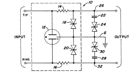
Referring now to the FIGURE l, there is
illustrated an electrical schematic representation of
an overvoltage protection circuit according to the
invention generally designated by the reference numeral
10. The overvoltage protection circuit 10 is adapted
for connection via TIP and RING conductors to a tele-
phone system or other similar communications source
at its INPUT. A subscriber's station, such as a key
set, modem or private branch exchange is connected to
the OUTPUT of the circuit 10. The overvoltage pro-
tection circuit 10 includes a gas discharge tube 12or similar device that is connected between the TIP
and RING conductors and to ground potential at ground
line G. A resistor 14 is cornected in series with
the TIP line and a resistor 16 is connected in series
with the RING line.
A transient voltage suppressor 18 is con-
nected between the resistor 14 and ground potential
and similarly a transient voltage suppressor 20 is
connected between the resistor 16 and ground potential.
The gas discharge tube 12 clamps transient voltages
that appear both across the TIP and the RING con-
ductors with respect to the ground line G and provides
--4--
a high impedance to the ground line G when a high
voltage transient is not present. A three electrode
gas discharge tube device such as, a Milli-Triac part
number MLTOO90, rated for a breakdown voltage of 600
volts, manufactured by Reynolds Industries may be
employed for the gas discharge tube 12. The transient
voltage suppressors 18 and 20 conduct whenever the
voltage potential applied to the TIP or RING lines,
respectively, exceeds a predetermined breakdown voltage
potential, for example, at 200 volts. The gas dis-
charge tube 12, resistors 14 and 16 and the transient
voltage suppressors 18 and 20 are enclosed in dotted
lines in the accompanying figure and are effective
for protecting the communications equipment from
hazardous voltages due to lightening and power surges.
Transient voltage suppressors of a type manufactured
and sold by General Semiconductor Industries, Inc., a
Square D Company under a registered trademark ~ransZorb,
such as part number SCM170C rated for a reverse stand-
off voltage without conduction at 170 volts and for abreakdown voltage in a range between 189-231 volts,
advantageously may be employed for suppressors 18 and
20.
A capacitor 22 and a transient voltage sup-
pressor 24 are connected in series between the ground
line G and a junction 26 of the series connected re-
sistor 14 and transient voltage suppressor 18. Simi-
larly, a capacitor 28 and a transient voltage suppres-
sor 30 are connected between the ground line G and a
junction 32 of the series connected resistor 16 and
transient voltage suppressor 20. Similar devices as
used for the transient voltage suppressors 18 and 20
advantageously can be employed for the suppressors 24
and 30, except having a lower breakdown voltage rating,
such as part number SCM5.0C with a breakdown voltage
rating in a range between 6.4 - 7 volts or part number
SCMlOC with a breakdown voltage rating in a range
1~681~
--5--
between 11.1 - 13. 6 volts. The transient voltage
suppressors 24 and 30 are selected to have a breakdown
voltage rating above a predefined potential of a data
signal carried by the TIP and RING conductors, such
as, for example, 5 volts or 10 volts.
In operation, the series connected resistor
14, capacitor 22 and transient voltage suppressor 24
suppress noise and transient voltage signals having a
predefined threshold rate of change and that are above
the breakdown potential of the suppressor 24. This
predefined threshold rate of change or frequency re-
sponse is determined by the component values of the
resistor 14 and capacitor 22. For example, capacitors
22 and 28 may be provided in a range of 0.1 and 1
15 microfarad with resistors 14 and 16 selected in a
range between 10 and 30 ohms. Otherwise, in normal
operation data signals are unaffected by the frequency
response of the filter comprised of resistor 14 and
capacitor 22 with the suppressor 24 blocking current
20 flow. Similarly, the resistor 16, capacitor 28 and
transient voltage suppressor 30 clamp noise and tran-
sient voltage signals occurring on the RING line.
Referring now to FIGURE 2, there is shown
an alternative embodiment of an overvoltage protection
25 circuit according to the invention generally designated
by the reference numberal 10'. The same reference
numerals are used for similar components of FIGURE 1.
The protection circuit 10' includes a star arrangement
of unipolar transient voltage suppressors 34, 36 and
38. The transient voltage suppressors 34, 36 and 38
perform the same function as the bidirectional sup-
pressors 24 and 30 as before described. Unipolar
transient voltage suppressors are available from
General Semiconductor Industries, Inc. also sold under
35 the registered trademark TransZorb as device types
SCM5.0A through SCM170A .
In both protection circuits 10 and 10', the
gas discharge tube 12 can be omitted. In addition,
~868~2
--6--
both protection circuits can be provided without the
bidirectional transient voltage suppressors 18 and
20. It should be understood that the gas discuarge
tube 12 and the suppressors 18 and 20 can be eliminated
and the protection circuits 10 and 10' remain effective
for suppressing noise and transient voltage signals
above the data signal.
Although the present invention has been
described in connection with details of the preferred
embodiment, many alterations and modifications may be
made without departing from the invention. Accordingly,
it is intended that all such alterations and modifica-
tions be considered as within and spirit and scope of
the invention as defined in the appended claims.