Note: Descriptions are shown in the official language in which they were submitted.
1~37117
CONTROL D~VIC~ ~OR COO~ING ~PP M ~SVS
~CKGROVND OP THB INV~N~ON
1 ~ield of the lnventlon
Shi~ lnventlon relate~, ln general, to eooklng
appar~tu~ Hore peclflcally, the lnvention relate~ to a
eontrol panel for a eooklng apparatu~ through ~hich a u~er
nay lnput de~lred eooklng eonditlon~, ~uch a~, e 9 , eooklng
tlne or de~lred eookln~ node
2 De~crlptlon of the prlor art
Well known eooklng apparatu~, uch as nlcro~ave oven~,
typlcally are provlded with a control panel ~ plurality of
eooklng eonditlon key~, ~uch a~, e g , ~ ~tart key, a cancel
key, a plurallty of eooking node key~, ete noraally are
arran~ed on the eontrol panel
~n exa~ple of the bove-de~crlbed control panel 1~
di~elo~ed ln ~ S P ~ S,S8~ ued on Mar 20, 1979 ln the
naae Or Jon ~ Otterlel, and entitled ~L~XIBL~ K~Y~OARD
SWITCH WITH INT~GR~ SP~C~R PROTRUSIONS In thl~ prlor art,
a plurallty of eooking eondltlon et key~ ~ncludlng -
plurality of eooklng node key~, a eaneel key, a ~tart key
ete , are provided on one lde of a fold llne of a Hylar
heet A plurality of eonductlve area~ eorresponding to the
eooklng eondltlon et key~ are arranged on the correspondln~
rear urfaee of the Mylar heet ~ key-natrlx eireuitry
eonprl~es tho~e eonduetlve reas eonnected to one another
plur-llty of key cannlng ignal llne~ eonnected bet~een
tbe key-natrlx elreultry and a naln eontrol eetlon are
foraed on the rear urface of tbe Mylar he-t a plur~llty
* Trademark
_ ~ _
~,
~ '
:~ '
~2~3~7
of conductlve ele~ents corre~pondln~ to the conductlve ~rea-
are provlded on the rear urface of the Mylar hcet at the
opposlte lde of the fold llne fron the et key~ ~ach
conductlve ele~ent lncludes a palr of terninals ~ kcy
~ignal llne forned on the oppo~ite slde of the rear urface
ls connected to each conductive ele-ent When thc heet ls
folded along the fold line, each conductive rea of one ~ide
urface and the corresponding conductive ele~ent cone lnto
appo~itlon, to act as a flxed contact of a nornally open
single-pole ~in~le-throw switch For exa~ple, when a
desired key ls pressed, the corresponding conductive area
co~es into contact with the opposite conductive ele~ent
Therefore, the conductlve area ~akes the pair of terninals
of the conductlve elenent electrically contact with one
another therethrough
In this arrange~ent descr~bed above, since a large
nu ber of si~nal llnes are provided on one sheet, the
arran~enent of those signal llnes is co~plicated, and a
large ~heet ls needed for arranglng those signal llnes and
the cooking conditlon et keys
S~MM~RY OF TN~ INVENTION
It ls an ob~ect of the present lnventlon to slnpllfy
the con~tructlon of an lnput panel for a cooklng apparatus
To acconplish above object, the cookin~ apparatus
lnclude- a control panel wherein a flexible panel ls
provided a plurality of ¢ooking condltion set key-patterns
~re forned on the flexible panel When a deslred cookln~
condition et key-pattern ls operated, the flexlble panel
outputs a voltage correspondlng to the deslred cooklng
- 2 -
'
1~71~7
condltion ~et key-pattern The volt~e output fron the
flexible panel i~ changed ~tep by tep fro~ one ~lde ~ey
pattern ~f the cookln~ conditlon ~et key pattern~ toward the
other side key-pattern
The cooking condition ~et key-pattern~ ~ay lnclude a
cooklng tl~e ~cale pattern for lnputting a desired cooklng
tine
BRI~F D~SCRIPTION OF TH~ DRAWINGS
The present invention t~ be3t under~tood with reference
to acco~panying dr~wing~ in which
FIG~R~ a per~pective view lllu~trating one
enbodi~ent of the pre~ent invention;
FIGURB 2 is an enlarged plan view illustrating an input
panel a~ shown in FIGUR~ l;
FIGUR~ 3 ls a cross-~ectional view taken on line III-
III of Figure 2
FIGUR~ ~ is a view for explaining the operation of the
lnput panel shown in FIG~RE 2 and 3;
FIGUR~ 5 i~ a circuit dia~rao of the enbodi~ent shown
in FIG~R~ l;
FIGUR~ 6 l~ a ~raph ~howing the relationship between
cooklng condition ~et key-pattern and cach value of the
digital ~ignal of an ~/D converter ~hown in FIGUR~ 5;
FIGUR~ 7 ls a scheuatic vi-w of a ~econd enbodiuent of
thc pro ent invention;
FIG~R~ B is a per~pective vlew illuQtratlng a third
enbodinent of the pre~ent invention;
FIGUR~ 9 is an enlarged plan view lllu~trating an input
panel, a~ hown ln FIGUR~ 8;
~2~37117
FIGURE lO 1~ ~ clrcult dl~or of tbe thlrd e~bodluent
h~wn ln FIG~JR15 8; ~nd
FI¢UR~ a graph ~howlng the relatlon~hlp bet~een
cooklng ¢ondltion et key-pattern and each value of the
s di~ital ~l~nal of an ~/D converter hown ln FIGUR~ lO
D~AIL~D D~SCRIPTION OF TH~ PR~F~RR~D ~MBODIM~NTS
The preferrcd e-bodi~ents of the pre-ent lnventlon ~lll
now be de~crlbed ln nore detail ~ith reference to the
acconpanying dra~lngs
FIG~R~ a per~pective view of a uicrowave oven
nlcrowave oven 11 ls provided with a cooking cha~ber (not
~hown) therein a front door 13 i~ hln~ed at the front aide
of nicrowave oven 11 to open and clo~e the cooking cha~ber
In ~eneral, front door 13 includes a tran~parent panel 15 to
cnable a u-er to ~ee food dl~po~ed ln the cooking chanber
durin~ cooklng ~ bandle 17 1~ provided on the ~ide of
tran~parent panel 15 oppo~ite to the hlnged portion of front
door 13 ~n operatlon panel 19 18 provided on the front
~ide of nicrowave oven 11 ad~acent to front door 13
Operatlon panel 19 1~ provided wlth an lnput panel 21 for
lnputtlng de~lred cooklng ondltlons Operatlon panel 19
al~o l- provlded ~lth a digltal dlaplay 23 for dl~playln~
cookin~ lnfornatlon, uch a~ the lnputted de~lred cookln~
ode ~ tlner knob 25 al~o 1~ provlded on operatlon panel
19 for ~ettln~ a de~ired cooklng tine
~ hown ln ~IGUR~ 2, lnput panel 21 lnclude~ an
elongated ela~tlc heet 27 on ~hich a plurallty of cooking
conditlon ~et key-pattern- 29 are forned The cooklng
condltlon key-pattern- re arranged at prescrlbed lnterval-
"
., ,;.
12~7117
along the elon~ated dlrectlon of heet 27 Cookingcondltlon key-patterns 29 lnclude cooklng uode keys, a
cookln~ tart key, etc ~lastlc elon~ated cheet 2~ ls
provlded ~ith an elongated hollow port~on ~1 thereln A
5 flexible electric conductlve layer 33 1- provlded, ln the
elongated direction of sheet 27, on the one ~urf~ce of
hollow portlon 31 corresponding to the front urface of
~heet 27 The cooklng conditlon ~et key-patterns 29 are
forned thereon, as shown ln ~IGUR~ 3 Conductive layer 33
ls rorued ln an arc-shape ~n elongated plate-shaped
reslstor 35 i~ provided on the othcr surface of hollow
portlon 31 opposite to conductive layer 33 A conductlve
lead pattern 37 also ls provided in elongated sheet 27 ln
parallel to plate-shaped resi~tor 35, as shown in FIGURES 2
and 3 One end of plate-shaped resi~tor 35 i~ connected to
lead pattern 37, and the other end thereof is ~rounded for
applying DC voltage +V to resistor 35 through lead pattern
37 A ter~lnal 39 ls connected to one side of conductive
layer 33 Input panel 21 with the above-described
construction ls arran~ed on operation panel 19 such that the
front urface of elastic sheet 2~ ls flush wlth operation
panel 19
As can be understood fro- ~IG~R~ ~, when a desired
cooklng conditlon et kcy-pattern ls pressed, the portlon of
conductlve layer 33 corresponding to the desired cooking
conditlon set key-pattern deforas, ~nd co-es lnto contact
wlth the corresponding portlon of resistor 35 ~s a re~ult,
a prescribed voltage Vo is produced between terninal 39 and
the other lde (~rounded lde) of re~lstor 35
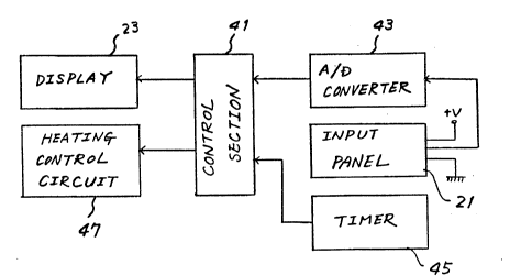
FIGUR~ 5 is a control block dia~ra~ of the above-
- 5 -
.
.
~ 2~7117
de~cribed oven ~ey~ nal data fro~ lnput panel 2l i~
lnput to a control eectlon ~l through an ~/D
(analo~/digital) converter ~3 Control ection ~l lncludes
a ~icroco~puter and lts peripheral control unit Cookln~
tine data ~et by tlner knob 25 ls lnput fron a nechanical
tl~er ~5 to control ection ~l Control ~ectlon ~l control~
di~play 23 for di~playing the de~ired cooking ~ode or other
cooking infor~ation Control section 4l al~o control~ a
heating control oircuit 47 for controlllng output of a
nagnetron (not ~hown) in accordance with those lnput data
A~ ~hown in FIG~R~ 6, when each cooking condition ~et key-
pattern is pres~ed, the corresponding digital ~gnal (Sa,
Sb, Sc, , or Sz) i~ ~enerated fro~ A/D converter ~3
The relation~hip between each cooking condition key-pattern
and the corresponding digital ~ignal (hereinafter referred
to a~ K~Y TABL~) i9 prevlously ~tored in a ROM tread only
~e~ory) in control ~ection 4l
The operation of the above-described con~truction will
be de~cribed hercafter First, food i~ put in the cooking
cha~ber of oven ll When the u~er pre~e~ a desired cooklng
xode key-pattern arranged on input panel 2l, A/D converter
~3 outputs the digital ~ignal corresponding to the voltage
Vo produced fron input panel 21 The uicroco~puter of
control ~ection ~l receive~ the digital signal, as de~cribed
above According to the digital ~ignal, the ~icroco~puter
read3 out the desired cooklng node fro~ the ROM in which the
K~Y TABL~ is ~tored For exa ple, the de~ired cooking ~ode
i~ di~played in dioplay 23 In accordance with the cooking
xode read out fron the ROM, the ~icroconputer energize~ the
~agnetron through heating control circuit ~7
~'
-- 6 --
~ ccordin~ to the nbove-described enbodinent, lnput
panel 21 eonprl~es elon~ated flexlble conductlve layer 33
and elon~ated plate-~haped resistor 35 oppo~ite to one
another. ~he voltage Vo between layer 33 and rcsi~tor S5
varles ln accordance ~ith the po~ition at ~hich conductlve
layer 33 contacts with resi~tor 35 when a de~ired cookin~
condition ~et key-pattern i~ pre~ed Based on the voltage
Vo fro~ lnput panel 21, A/D converter ~3 generates the
corresponding digital ~ignal Therefore, since a large
nunber of ~ignal lines of the above-de~cribed prior art are
elininated, the con~truction of the inut panel ay be
~i~pllfied In addition, the nanufacturing cost of an input
panel ~ay be reduced
FIGUR~ 7 is a ~chematic view illu~trating a ~econd
e~bodiment of the pre~ent invention In this enbodi~ent, a
plurality of cooking condition ~et key-patternc are provided
on operation panel 19 A plurality of pres~-bar ele~ents 51
corresponding to cooking condition ~et key-patterns
perpendicularly pro~ect fron the rear ~urface of operation
panel 19 at pre~cribed lntervals The area around each
pres~-bar elenent 51 of the rear ~urface of operation panel
lg i~ concaved toward the front surface thereof to easily
reciprocate press-bar elenent 51 Conductive layer S3 i~
posltloned apart therefro~ between oper&tlon panel 19 and
re~istor 35
In the second enbodinent described above, when a
desired cooking condition ~et ~ey-pattern on operation panel
19 is pressed, pre3~-bar element 51 co~e~ in contact with
conductive layer 33 at a point Therefore, conductive l-yer
33 and re~i~tor S5 produce one voltage Vo correspondin~ to
- 7 -
~ 2~37117
each pre~-bar elenent 51 of cooklng ¢ondltion et key-
pattern A~D converter ~3 outputs ~ dl~ital ~l~nal b-~ed on
the voltage Vo Accordingly the uicrocouputer of control
~ection ~1 uay exactly ldentify the de~ired cookln~
condition on the basis of the digital signal fed fro~ ~/D
converter ~3
FIGUReS B, 9, 10 and 11 show a third e~bodinent of the
prescnt invention In th$s third e~bodiuent, the cookin~
tlne scale pattern 61 of a cooking tiner ls provided on
elastlc sheet 2~, instead of echanical ti~er ~5 shown ln
FIGUR~ 5 ~Q shown ln FIGUR~ 11, ~hen the u~er pres~es a
desired portion of the tine scale pattern, the correQponding
voltage Vo is produced between conductive layer 33 and
resistor 35, as described before A/D converter ~3 provide~
a digital ~ignal (Stl,~ ------, or St60) representing the
desired cooking tlne to control section ~1 after receiving
the voltage Vo fron input panel 21 After that, as
describcd above, the uicrocouputer of control section ~1
control~ the oQcillating period of the nagnetron through
heatlng control circuit ~7 in accordance ~ith the digital
signal fron A/D converter ~3 representing the desired
cooklng tlae
Wlth the tblrd enbodlnent described above, since the
cooking tiae set function ls provided on the input panel, -
aechanlcal ti~er nay be ell~inated, and the construction ofa cooking tl-er aay be sl-plified further
In the tbird enbodi-ent, a tenperature scale pattern
for inputting desired tenperature data uay be provided on
the lnput panel ~urther-ore, it ay u~e onc cale pattern
both s a oooklng tiae cale and a teaperature cale
- 8 -
~ ~171~7
The pr~c~nt lnvent~on h~s been de~crlbed ~lth ra-pect
to pectflc e~bodi~ent~. ~o~ever, other oubodinent~ ba~ed
on the principlc~ of the pre~ent lnvention ~ill be obvlou~
to tho~e c~f ordim~ry klll ln the ~rt. Such e~bodl~ent~ re
5 lntended to be covered by the clai~