Note: Descriptions are shown in the official language in which they were submitted.
ll lZ~371~
ELECTRIC DISCHARGE MACHINING APPARATUS
BACKGROUND 0~ TNE INVENTION
l. Field of the Invention
This invention relates generally to a discharge machin-
ing apparatus for machining a workpiece by electrical dis-
- 5 charge into desired dimensions and surface roughness, and
more particularly to a discharge machining apparatus a-
dapted to realize improvements in electrode consumption
and in the surface quality of the machining surface.
.,~ 2. DescriDtion of the Prior Art
In a discharge machining apparatus in which a wor~piece
~ ls machined by electrical discharge caused by appIying a
d-c voltage across an electrode and the workpiece, the
electrode is inevitably worn out so long as discharge is
; ^ maintained. It hàs been experimentally confirmed that
there ls a relationship as shown ln Fig. 5 among the
perlod in which a discharge current flows as a d-c voltage
ls applied ln the form of pulses, or the width of the
discharge current pulse; the value of discharge current;
and the amount of electrode consumption. In other words,
if the discharge current value Ip is constant, the lower
- - the discharge current pulse width the higher becomes elec-
trode consumption. And, if the discharge current pulse
width is constant, the higher the discharge current value
Ip the higher becomes electrode consumption, -
In a discharge machining apparatus of a conventional
, ~ ~,,
type, therefore, a discharge voltage pulse V and a dis-
, charge current pulse I are usually set as shown in Fig. 4.
That is, discharge machining is performed by setting the
discharge current value Ip and the discharge current ON
~g
- 2 -
' "'
~ ' ,
~2~7~
duration TON at such values that electrode consumption
can be minimized within a permissible range where energy
can be maintained at a level required for discharge
machining. Now, supplementary description will be made,
referring to waveforms shown in Fig. 4. The waveform of
the discharge voltage V steeply rises at the initial
stage and then lowers stepwise in the later stages
because a voltage application does not necessarily
initiates discharge. SON refers to the duration in
which a voltage is applied, i.e., the ON duration of the
discharge voltage pulse, while SOFF to the duration in
which the voltage is not applied, i.e., the OFF duration
of the discharge voltage pulse. ToFF denotes the
duration from the time when the discharge current stops
flowing to the time when the next voltage is applied.
With the prior art, however, electrode consumption
can be reduced so long as discharge is performed
properly. In the actual discharge machining, an
abnormal phenomenon, such as an instantaneous
interruption of discharge current or an electrical
shortcircuiting between the electrode and the workpiece
often occurs. When any of such abnormal phenomena takes
place, the prior art has the following problems.
(Problems associated with the instantaneou-~ interruption
of discharge current)
As it now will be necessary to refer to the
drawings, these will first be briefly described as
follows:
Fig. 1: Waveforms of discharge voltage and discharge
current pulses in an embodiment of this
invention
Fig. 2: Waveforms of discharge voltage and discharge
current pulses with the prior art in the event
of an instantaneous interruption of discharge
current or an electrical shortcircuiting
between the electrode and the workpiece
Fig. 3: Waveform when discharge current is cut off
with the prior art in the event of an
instantaneous interruption
Fig. 4: Waveforms of discharge voltage and discharge
current pulses with the prior art
Fig. 5: Diagram of assistance in explaining the
relationship between discharge current pulse
width and electrode consumption
Fig. 6: Main circuit of the first embodiment of this
invention
Fig. 7: Control circuit of the first embodiment of
this invention
Fig. 8: Circuit for generating a control circuit
signal in th~ first and second embodiments of
this invention
Fig. 9: Waveforms relating to Fig. 8
Fig. 10: Circuit for detecting the state of discharge
Fig. 11: Diagram of assistance in explaining the method
of detecting the state of discharge
Fig. 12: Waveforms relating to Figs. 6 and 7
Fig. 13: Main circuit of the second embodiment of this
invention
Fig. 14: Control circuit of the second embodiment of
this invention
Fig. 15: Diagram of assistance in explaining the
operation of the resistor RD in Fig. 13
The waveforms of the discharge voltage pulse V and
the discharge current I when discharge is normally
maintained are as shown in Fig. 4.
It sometimes happens, however, that discharge is dis-
3a
,~.
.
~ ~2~7~
continued for some reason, such as a sudden widening ofthe machining gap, reducing the discharge current to zero
(i.e., leading to an instantaneous interruption).
The change in the discharge voltage pulse V and the
discharge current pulse I in this case are shown in Fig.
2A. Since the ON duration of the discharge current pulse
I is kept constant with the prior art, the instantaneous
interruption divides the discharge current I into two
parts. This means that a discharge current pulse I is
"~ 10 divided into two successive pulses having narrower widths,
with the magnitude thereof remaining unchanged. If the
;j pulse width is reduced with the magnitude thereof kept
constant, electrode con8umption is increased, as described
earlier, referring to Fig. 5. To avoid a successive
generation of narrower-width pulses, the method of turning
off the discharge current upon detection of an instanta-
~, neous lnterruption has been conceived. The method of
merely turning off the discharge current, however, cannot
prevent a,narrower-width pulse having the same magnitude
from being produced, though a succession of such pulses
can be prevented to be sure. This method has proved
unpractical because of the resulting high electrode con-
sumption.
Furthermore, when pulses having narrow widths are kept
produced sucessively as with the prior art, a sort of arc
discharge may result. In such an arc discharge, unwanted
by-products, sùch as tar, of machining may be deposited on
the machining part, making the subsequent machining un-
stable and causing further instantaneous interruptions.
As described above, the prior art has a problem of
accelerated electrode consumption in the event of instan-
taneous interruption of discharge current.
(Problems associated with electrical shortcircuiting)
An electrical shortcircuiting may occur between the
electrode and the workpiece in the course of the ON dura-
tion of the discharge current pulse I due to the reduced
gap between the electrode and the workpiece or other
reasons. Fig. 2B shows the change in the discharge vol-
.,~ tage pulse V and the discharge current pulse I in the
event of electrical shortcircuiting. With the prior art,
the discharge current pulse I ls maintained for a prede-
termined duration, causing a shortcircuit current to flow
during the period from the start of shortcircuiting to the
end of the predetermined duration. This shortcircuit
current may deteriorate the quality of the machining sur-
face of the workpiece.
That is, the prior art has a problem of the deterio-
rated quality of the machining surface caused by the con-
tinued flow of a shortcircuit current in an electrical
shortcircuiting.
As a means to overcome this problem, it may be con-
ceived that upon detecting a shortcircuiting, the dis-
charge current pulse I is forcibly cut off immediately to
prevent a shortcircuit current from flowing. With this
arrangement, however, a discharge current pulse I having a
narrow width could result, increasing electrode consump-
tion.
Consequently, a technology of eliminating an instan-
taneous interruption or electrical shortcircuiting, which
1~371~9
may adversely affect discharge machining, without
causing increased electrode consumption or deteriorated
machining surface of a workpiece has long been desired.
This invention is intended to meet such a need.
SUMNARY OF THE INVENTION
It is an object of an aspect of this invention to
provide a discharge machining apparatus which is adapted
to cut off the supply of discharge current, in the event
of an electrical shortcircuiting of electrode, or an
instantaneous interruption of discharge current during
discharge machining, without causing increased electrode
consumption.
It is an object of an aspect of this invention to
realize the foregoing object by immediately eliminating
such an abnormal state as an electrical shortcircuiting
or an instantaneous interruption of discharge current to
prevent the quality of the machining surface of a
workpiece from deteriorating.
An aspect of the invention is as follows:
A discharge machining apparatus having a discharge
current control means for controlling a discharge
current flowing between an electrode and a workpiece as
a result of the application of a d-c voltage, a
discharge current value setting means for setting the
value of said discharge current, such that said value
rises in a special manner and a discharge current pulse
width setting means for setting the pulse width of said
discharge current, in which said discharge current
control means carries out discharge machining by
controlling said discharge current in accordance with a
discharge current value set by said discharge current
value setting means and a discharge current pulse width
set by said discharge current pulse width setting means;
characterized in that an abnormal mode detecting means
for detecting an instantaneous interruption of s~id
,, .
7~19
discharge current taking place during an ON duration of
said discharge current pulse, and a forced cut-off means
for cutting off the supply of said discharge current for
a predetermined period of time immediately after said
S abnormal mode detecting means detects the occurrence of
said instantaneous interruption is provided; said
discharge current value setting means being adapted to
set a discharge current value which is gradually
increased with the lapse of said discharge current pulse
ON duration; whereby the maximum value of said discharge
current during said ON duration being reduced when said
instantaneous interruption occurs.
By way of added explanation, the invention in an
aspect thereof comprises a discharge current value
setting means for setting a discharge current value in
such a manner that the discharge current value is
gradually increased in accordance with the lapse of the
ON duration of the discharge current pulse, an abnormal
mode detecting means for detecting an electrical
shortcircuiting or instantaneous interruption, and a
forced cut-off means for cutting off the supply of
discharge current for a predetermined duration
immediately after the abnormal mode detecting means
detects such an electrical shortcircuiting or
instantaneous interruption.
Since the discharge current value setting means
sets the discharge current value in a gradually
increasing fashion, electrode consumption is not related
to the length of the ON duration of discharge current
pulse. Thus, the discharge machining apparatus can cut
off the supply of discharge current immediately upon
detecting an electrical shortcircuiting or instantaneous
interruption of discharge current, preventing the
surface quality of a workpiece from deteriorating.
~2~37~
DESCRIPTION OF THE PREFERRED EMBODIMENTS
In the following, preferred embodiments of this
invention will be described in detail, referring to the
accompanying drawings.
This invention has such a construction that the
value of discharge current is gradually increased in
accordance with the lapse of the ON duration of
discharge current pulses, taking into account the
relationship between the pulse width of discharge
current and electrode consumption (refer to Fig. 5), and
that when an instantaneous interruption of discharge
current takes place, the discharge current pulse is
immediately cut off for a predetermined duration.
First, the operation of this invention will be des-
7~
cribed, referring to Fig, 1. Fig. lA sh~ws the state
where discharge is performed normally. V1 in Fig. lA
refers to a discharge voltage pulse when discharge is
being performed normally, and I1 to a discharge current
pulse at that time, which is gradually increased with the
lapse of time. Both pulses change minutely for a while
after the start of discharge due to minimal changes in the
state of discharge. V2 in Fig. lA refers to a discharge
voltage pulse when an instantaneous interruption of dis-
charge current has occurred, and I2 to a discharge current
"~ pulse at that time. Upon detection of an instantaneous
interruption of discharge current, the applica~ion of
power is immediately discontinued, and resumed after the
lapse of a predetermined time. V3 and I3 indicate dis-
charge voltage and discharge current pulses during the
. next discharge.
V2 in Fig. lB is a discharge voltage pulse when a
shortcircuiting has occurred, and I2 a discharge current
pulse at that time. Upon detection of a shortcircuiting,
the application of power is immediately stopped, and re-
sumed after the lapse of a predetermined time. Vl and Il,
and V3 and I3 in Fig. lB are discharge voltage and dis-
charge current pulses during normal discharge before and
after a shortcircuiting, respectively.
Z5 Next, why the increase in electrode consumption or the
deterioration of the surface quality of the workpiece
caused by an electrical shortcircuiting or an instanta-
neous interruption of discharge current can be prevented
by employing this invention having the aforementioned
construction and operation will be described.
37~9
Setting the discharge current pulse in such a manner
that the value of discharge current is gradually increased
with the lapse of time means that the electrode consump-
tion characteristic curve shown in Fig. S is shifted
S continuously from a curve having a small current value to
another curve having a larger current value, one by one,
with increases in the width of the discharge current pulse
I (that is, as the coordinates advance in the direction of
~ the abscissa axis). By selecting the time elapsed from
" 10 the start of the discharge current pulse (the abscissa l'1,
T2 ~~~) and the value of discharge current (Ipl, Ip~ ---)
so that the tra~ectory of shifting points becomes parallel
with the abscissa axis, as shown by dotted lines in the
figure, electrode consumption is kept at all times at a
predetermined value M even when the discharge current
pulse is turned off at any point of time in the course of
discharge .
Consequently, when the discharge current pulse is imme-
diately cut off at any point of the discharge current
pulse I, upon detection of an instantaneous interruption
or a shortcircuiting, an increase in electrode consumption
can be prevented. Since the discharge current pulse can
be immediately cut off in the event of an instantaneous
interruption of discharge current or a shortcircuiting
without regard to electrode consumption, the roughening of
the surface quality of the workpiece can be eliminated.
In the following, the construction of this invention
will be described more specifically.
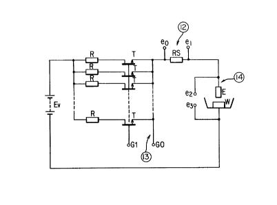
Fig. 6 shows the main circuit of a first embodiment of
this invention. In Fig. 6, T indicates a transistor; R a
' _ ~o_
'
,
t3711~3
derating resistor for the transistor T; RS a current
detecting resistor (or a current detector using a Hall
element); E an electrode; and W a workpiece, respectively.
Each of series circuits comprising the resistors R and the
transistors T almost equally shares a current, and the
magnitude of the current is controlled by changing the
internal resistance of the transistor T by a control
signal. A control signal is produced by comparing the
discharge current detecting signal detected by the current
"~ 10 detecting resistor RS with a reference value which is
set in advance so that the discharge current is increased
gradually. Using the resulting control signal, the tran-
sistor T is controlled. As a result, the discharge cur-
rent pulse assumes a waveform in which the current value
~- 15 increases gradually as desired. A control circuit for
producing this control signal is shown in Fig.7.
In Fig. 7, Pl and OP2 indicate operational amplifiers;
D/A a digital/analog converter; and C6 a counter, respec-
tively. The output ( ~ ) of the digital/analog converter
D/A is thë aforementioned gradually increasing reference
value, with which the discharge current detecting signal
~ entering from terminals el and eO is compared, and a
control signal for controlling the transistor T is trans-
mitted from terminals Gl and Go~ The gradually increasing
reference value is produced by the digital/analog con-
verter D/A and a ROM as the preceding stage thereof, the
counter C6, etc. The counter C6 is caused to operate by
a ToFF end signal ~ , a TON end signal ~ , and a clock
~ . (These signals are generated in the circuit shown in
Fig. 8.) The counter C6 is cleared with the ToFF end
119
signal ~ prior to the start of one discharge current
pulse. Then, the counter C6 starts counting up sequen-
tially by counting the clock ~ which is inputted as
discharge begins. The ROM transmits to the digital/analog
converter D/A the information on the discharge current
stored in the addresses designated by the counts counted
by the counter C6 that counts up. In this way, a gradual-
ly increasing reference value is produced. An ALL.F data
is loaded on the counter C6 by the TON end signal ~ to
.,~ 10 prevent the discharge current from flowing during the TQFF
duration. Waveforms of the signals designated by en-
circled numerals and symbols in Fig. 7 are shown in Fig.
12.
Fig. 8 8hows a circuit for generating a control circuit
;. 15 signal in the first embodiment and a second embodiment,
.. . ,, ,, ~, .
:; which will be described later (refer to Figs, 13 and 14),
~^ ~ - of this invention. With reference to the first embodi-
ment, the circuit shown in Fig. 8 is a circuit for produc-
ing the ToFF end signal ~ , the TON end signal ~ , and
the clock ~ required in Fig. 7. With reference to the
second embodiment, the circuit shown in Fig. 8 is a cir--
cuit for producing the abovementioned signals and a signal
. . ~ for telling the duration from the end of the ToFF
duration to the end of the next TON duration (that is, the
,~ 25 duration from the ToFF end signal ~ to the next TON
~f'~ ~ ' duration ~ ). In Fig. 8, C2 refers to a counter to which
the data on the length of the TON duration is set through
a bus 7-1, while C1 is also a counter to which the data on
the length of the ToFF duration is set through the bus 7-
~ FF1 ls a flip-flop for setting the TON duration, and
- 12 -
FF2 is a flip-flop for setting the ToFF duratlon. MV
through MV3 are multivibrators for shaping waveforms.
When a discharge start signal ~ enters the flip-flop
FFl, a logic element 7-5 is turned on by the output of the
flip-flop FFl, causing the clock to pass through the logic
element 7-5. The clock then partly goes out through ~ ,
and partly enters the counter C2 to count and decrease the
data set therein. When a predetermined value is reached,
a signal indicating the end of the TON duration (TON end
signal ~ ) is transmitted through a logic element 7-6.
At the same time, the TON end signal is fed to the flip-
. `flops FP1 and FF2. The flip-flop FFl-reverses the output
to turn off the logic element 7-5, preventing the clock
from passing. The flip-flop FF2, on the other hand, turns
~'~ 15 ` on the logic element 7-8, causing the clock to pass.~The
clock passing the logic elemene 7-8 ~-decreases -the`;---data
.- - set in th- counter C1. When a predetermined value ~is
reached, a signal indicating the end of the ToFp duration
(ToFF end signal ~ ) i6 transmitted. At the same time,
this signal is fed to the set terminal S of the flip-flop
. FF2 to set the flip-flop FF2, feeding the outout thereof
to the flip-flop FFl. Upon receiving the output, the
` flip-flop FF1 is put on standby in the state ready for
starting the counting of the aforementioned TON duration
as soon as the discharge start signal ~ appears. In
this way, the TON duration and the ToFF duration are set
- -to desired lengths, and if an instantaneous interruption
or a shortcircuiting occurs during discharge (that is,
during the TON duration), the following operations are
carr$ed out to immediately generate a TON end signal
- 13 - `
: :
,: . ~.,`'
3'~
(a signal to instruct DISCH~RGE END). During discharge, a
signal to turn on the logic elements 7-3 and 7-4 enters
the input terminals of any one of these logic elements
from the flip-flop FFl. When a shortcircuiting or an
instantaneous interruption occurs, a shortcircuiting de-
~ecting signal ~ or an instantaneous interruption de-
tecting signal ~ enters, causing the logic element 7-2
to generate an output to transmit a TON end signal ~ via
the logic element 7-6 and trigger the flip-flop FFl to
.,~ lO carry out the predetermined operations required to termi-
nate the TON duration. The data is set to the counters Cl
and C2 at the time when an input enters the L/D terminal
of these counters. The path containing the MV3 is a path
for passing a signal indicating POWER ON. At the outset
;.; 15 of POWER ON, a signal i8 fed to the L/D terminal of the
counter Cl through the logic element 7-9 to initiate a
ToFF duration.
and ~ shown in Fig. 9 are waveforms at portions
~ and ~ shown in Fig. lO, and the remaining ones indi-
cate waveforms at other portions indicated by the corres-
ponding symbols in Fig. 8.
Fig. lO shows a circuit for detecting the state of
discharge for detecting, by a change in discharge voltage,
whether discharge is started, or a shortcircuiting or an
instantaneous interruption occurs. The discharge voltage
is a vol~age across the terminals e2 and e3 shown in Fig.
6. Fig. ll is a diagram of assistance in explaining the
method of detecting the state of discharge by means of the
circuit shown in Fig. lO. V in Fig. ll indicates a
discharge voltage pulse when normal discharge is perform-
- 14 -
37~9
ed. The start of discharge is detected by knowing that
the magnitude of the discharge voltage becomes smaller
tha~ a predetermined voltage Vc. An instantaneous inter-
ruption is detected by knowing that the discharge voltage
becomes larger than a predetermined voltage VB. And, a
- shortcircuiting is detected by knowing that the discharge
voltage becomes smaller than a predetermined voltage Vc.
The circuit shown in Fig. 10 performs the abovementioned
detecting operations. A discharge voltage is applied to
"~ 10 the terminals e2 and e3, as described above. Comparators
COMPl through COMP3 compare the discharge voltage with
predetermined voltages Vc through VA, and generate a dis-
charge start signal ~ , an instantaneous interruption
detecting signal ~ and a shortcircuiting detecting sig-
lS nal ~ . These signals are used in the circuit shown in
Fig. 7-
: Fig. 12 ls a diagFam illustrating waveforms relating to
Figs. 6 and 7. The waveforms indicated by encircled nume-
rals and symbols in Fig. 12 are waveforms at portions
designated by the corresponding numerals and symbols shown
in Figs.~6 and 7.
Fig. 13 shows the main circuit of the second embodiment
of this invention. The first point different from the
first embodiment is that control transistors Tol through
. 25 T80 are subjected to an on-off control. The second dif-
ference is that the currents allocated to series circuits
having resistors Rol through R80 and transistors Tol
through T80 and comprising a control section are set to
have different magnitudes for the purpose of weighting.
With this arrangement, the magnitude of current is ad-
37~19
justed to a de~ired level by selecting a transistor being
turned on by a control signal (the circuit for generating
the control signal is shown in Fig. 14, which will be
described later.) The third difference is that an induc-
tor L, a flywheel diode FD, a damper resistor RD, and a
transistor TD are provided to carry out a flywheel opera-
tion in accordance with the on-off control. The flywheel
operation can prevent the intermittent breaking of the
" discharge current at the time of current value changeover.
As the control signal for the transistor TD, a signal ~
obtained in Fig. 8 is used to keep the transistor TD
turning on for a period when voltage is applied across the
electrode E and the workpiece W. The damper resistor RD
has a role of rapidly damping the waveform of the di-
scharge current at the end of the TON duration, as shown
- in Fig. 15.
Fig. 14 shows the control circuit of the second embodi-
ment. A counter C13 and a ROM in Fig. 14 serve the same
role as the counter C6 and the ROM shown in Fig. 7. On
the basis of a signal fetched from the ROM, a driver 13-1
transmits a control signal to the transistors To1 through
T80 shown in Fig. 13.
As described above, this invention makes it possible to
forcibly turn off the discharge current pulse immediately
ZS after an instantaneous interruption or a shortcircuiting
occurs because such a forced turning-off does not lead to
an increase in electrode consumption. Consequently, the
quality of the machining surface of a workpiece can be
prevented from deteriorating because such a forced
cutting-off does not develop into an arc discharge nor a
- 16 -
7 ~
continued flow of shortcircuit current for a long time.
- 17 -
: