Note: Descriptions are shown in the official language in which they were submitted.
C0440/7001WO
0324~I
PROGRAMMABLE LOCiIC CELL AND ARRAY
Field of the Invention
This invention relates to the field of digital
logic circuits and, more pàrticularly, to
programmable and reprogrammable logic devices, and a
graphics-oriented system for programming such
devices.
Backqround of the Invention
In the field of digital systems design,
considerable efforts have been directed towards
shortening product-development cycles. One of the
significant factors in the length of such product
deyelopment cycles is the time required for the
design and fabrication of digital integrated
circuits (IC's). Once a circuit design is
completed, it generally takes at least four weeks,
and often several months, to fabricate a silicon
version of the circuit in a "chip." To reduce the
design and fabrication interval, attempts have been
i
7~Z~
Co440/7001WO
--2--
made to provide various types of user-definable, or
programmable, logic devices (PLD's). Prior PLD' s
include, inter alia, programmed logic arrays (PLA's~
and gate arrays.
In the field of programmable logic, there are
generally four strata of integrated-circuit
customization available: ~1) fu'l custom IC's;
(2) standard-cell-based IC's; (3) mass-programmable
IC's, such as gate arrays; and (4) user-programmable
IC's, such as programmable logic devices. The first
two alternatives involve customization of all mask
layers required to manufacture the IC to the user's
specifications and are therefore often referred to
as "custom" IC design. The third alternative is
sometimes called "semi-custom" IC implementation
because only a few of the mask layers are customized
to the users' specifications. The fourth
alternative, user-programmable IC's, includes those
IC's in which no customization of mask layers is
required. The present invention falls into that
latter category. The trade-offs between these
various alternatives involve the time required to
bring a new product design to market, engineering
cost, expected unit volume, ease of use of design
tools and familiarity with the design methodology.
Until recently, PLD's generally could be
programmed only once, at the time of manufacture --
they were generally not reprogrammable. Such
programming has been accomplished by various
methods. In PLA's, fusible-link technology has been
12~37~
C0440/7001WO
--3--
employed, wherein"such links are "blown" open to
program ~hese devices. In gate arrays, a custom
metallization layer is deposited to interconnect the
logic elements and provide the programming.
Alternatively, a laser may be used to break
connections in a metalliza~ion layer. The most
significant limitation on these approaches is that
the device can be programmed only once. For
example, after an internal fuse has been blown, the
device cannot be reprogrammed. Further, since fuses
can only be blown once, PLD's can only be tested
destructively. Such testing methods naver allow for
full evaluation, so most us.ers of bipolar
programmable logic devices have rosorted to
extensive post-programming testing specif~c to their
applications. Additionally, a device which is only
programmable one time (i.e., at the factory or in
the field) must be discarded if a programming error
is discovered or a change of program is desired.
Recently, a new genre of user-programmable IC's
has been developed; these new IC's are
electrically-programmable and reprogrammable logic
devices, such as reprogrammable gate arrays and the
devlce and system of my US patent 4,700,187 issued
October 13, 1987 for "Programmable, Asynchronous Logic
Cell and Array." To emphasize the reprogrammability
of such components, they are sometimes called
"erasable, programmable logic devices," or EPLD's.
By contrast with earlier program-once technologies,
an EPLD can be programmed more than once; therefore,
C0440/7001WO
--4--
an error in programming can be corrected by simply
reprogramming the device. Further, since the
devices are reprogrammable, the entire device can be
fully, nondestructively tested at the factory; such
testing is independent of any device application and
therefore need not be the user's responsibility.
In general, an EPLD comprises an array of logic
elements and programmable means for interconnecting
~hose elements. The choice of logic elements made
available in the device, the interconnection
mechanism and the logical and physical layout of
components greatly influence the properties and
capabilities o an EPLD. Consequently, EPLD's
designed for one type of application may not be
optimal for another type of application.
The most common earlier approaches in
programmable logic devices, and a currently leading
approach in EPLD's, employ variations of the PLA
architecture, which is composed of an AND-array
connected to an OR-array. Most PLD's add to these
arrays input and output blocks containing registers,
latches and feedback paths. The connections between
the AND and OR arrays are programmable, as are the
input and output blocks and feedback paths.
Programmability of these connections is achieved
through the use of fusible links, EPROM cells,
EEPROM cells or static RAM cells.
. ~ ..... .... . . . .
371~_~
C0440/700lWO
--5--
Typical EPLD's are represented by the EPLD
models 5C031, 5C032, 5C060, 5C090, 5C121, 5C180 and
related devices of Intel Corporation, Santa Clara,
California, described in the Intel publication
titled User Defined Loqic Handbook EPLD Volume,
1986. Another good example of a programmable logic
device is the Logic Cell Array (a trademark) from
Xilinx, Inc. Both companies market EP~D's and
associated development systems which provide tools
to aid in the design of logic systems employing
their resp~ctive programmable devices.
The Intel devices employ an architecture based
on the "sum of products" PLA structure with a
programmable AND-array feeding into a fixed
OR-array. Design entry is accomplished by one of
four methods: (1) schematic input of the logic
circuit; (2) net list entry, by which the user
enters the design by describing symbols and
interconnections in words, following a standardized
format; ~3) state equation/diagram entry; and (4)
Boolean equations. Intel's development system
converts all design entry data into Boolean
equations which are then converted to a
sum-of-products format after logic reduction. The
configurable logic block used in the Xilinx product
is programmed either by the entry of Boolean
equations or by the entry of a Karnaugh map.
12~371~",
C0440/7001WO
--6--
While these EPLD architectures may represent an
advance over prior logic systems which did not
provide user programmability, they are far from
ideal. The requirement that Karnaugh ~aps and
Boolean equations be used to program these devices
means the user must have extensive training in
digital logic design. This, of course, limits the
user base. Neither does either approcch provide a
tool for the modular, hierarchical design of complex
circuits. Other deficiencies will be apparent to
those skilled in the art.
Accordingly, it is an object of the present
invention to provide a reprogrammable digital logic
device which can be programmed easily to implement a
large class of digital circuits.
Another object is to provide such a device which
is electrically reprogrammable.
It is a further object of the invention to
provide a programmable~ universal digital logic cell
or set of cells which can be employed to implement a
large class of digital circuits.
Yet another object of the invention is to
provide a computational apparatus and architecture
in which concurrency can be achieved at a very low
level of granularity.
371~
Co440/7001WO
--7--
Another object of the invention is to provide a
reprogrammable digital logic device which can be
programmed and reprogrammed easily to implement
self-timed logic systems.
Still another object of the invention is to
provide a method, based upon graphics operations, to
facilitate the programming of indiv dual EPLD's as
well as systems built up from a plurality of similar
EPLD's.
A still further object of the invention is to
provide a programmable logic device and a graphical
programming environment therefor, which together
support the modular, hierarchical construction of
logic circuitry by means of block diagrams.
Yet another object of the invention is to
provide a programmable logic device and a
development system therefor, which support the
translation, rotation and reflectior, of logic
circuits and circuit blocks as part of the process
of designing a system with one or more of such
devices.
Summarv_of the Invention
These objects are achieved in the present
invention by the use of particular programmable
logic cells, and arrays of those cells, having
certain characteristics. These characteristics
.. .
~ ~71~
C0440/700lWO
--8--
include, inter alia, the following: (1) the ability
to program each cell to act either as a logic
element or as one or more logical "wiee~' elements
(i.e., identity functions between one or more
specified inputs and one or more specified outputs
of the cell -- these identity functions include
crossovers, bends, fan-outs, and routings running
both horizontally and vertically); (2) the ability
to rotate circuits (through 90 increments) and to
reflect circuits about horizontal and vertical axes;
(3) an integrated logic and communication structure
which emphasizes local communications; (4) a simple
structure at the cell level, thereby making
available a very fine-grained logic structure; and
~5) suitability for implementation of both
synchronous and asynchronous logic, including
spéed-independent circuits.
In an exemplary implementation, each cell has
two inputs and two outputs, allowing the cells to be
arranged in a grid such that each cell communicates
with its north, east, south and west neighbors. The
cells are programmable to assume any one of several
states, to provide the foregoing characteristics.
Such arrays of cells are well-suited to
implementation in an integrated circuit "chip" using
modern, very-large-scale integration (VLSI). On a
chip, the logical wiring capabilities of the cells
make it possible to "wire around" defective cells
C0440/7001WO
_g _
and elements. Thus, the inventlon shows promise for
so-called "wafer-scale" integration or fabrication.
If a large wafer contains a few defective cells,
those cells can simply be avoided and bypassed, with
the remainder of the wafer remaining useful. This
may permit the fabrication of much larger chips than
has heretofore been possible, since defects normally
render a chip useless.
These chips can themselves be assembled into
arrays and other configurations. Such an arrangment
of cells (whether disposed on one or more chips) may
be referred to as a "medium." For contrast and
clarity of expression, an array of chips will be
referred to hereinafter as a "matrix," to
distinguish from an array of cells. A matrix of
chips can be extended freely in any dimension
desired. Thus, computing power can be increased by
simply adding more chips to the matrix.
The basic logic cell is programmable and
reprogrammable in accordance with existing
technology adaptable to that purpose. Programming
is accomplished by setting the states of an
appropriate number of storage (i.e., memory)
elements associated with each cell. In a first
exemplary embodiment, the cells may be composed of
NOR gates, transistor switches and gain elements for
driving adjacent-cells. The gain elements .~ay be
., . , . ., ., , . ,, . _ ... _ , _ , ., _ . . . .. . .. . . . ...
~L2 ~71~d
Co440/7001WO
--10--
inverters or tri-state devices; the latter may also
provide the switching functions.
A reduction in cell complexity and increase in
cell speed may be achieved by composing the medium
from two types of cells which alternate with each
other. The two types of cells may differ from each
other only in that inverters are added on the inputs
of the cells of a first type and on the outputs of
the cells of the second (i.e., other) type. The
inverters, though not providing logical function,
cannot be eliminated, since they provide needed gain
for logical wires. Since these inverters occur in
pairs, their addition does not alter the logical
operation of the array; indeed, as far as the user
is concerned, the inverters may be ignored and the
array may be dealt with as if it contained only one
kind of cell.
The invention provides a general-purpose
architecture for computation and digital systems.
Using a programming system such as the exemplary
graphical programming environment described below,
the individual logic cells may be programmed and
connected together to implement an extensive class
of logic circuits. Further, different cells on the
same chip may operate concurrently and even
independently of each other. Configurations for
(i.e., programs for setting cell storage elements to
create) circuit blocks such as adders, multiplexers,
~2371~
-- 1 ].
buffer stacks, and so forth, may be stored in a
library for use in building more complex blocks.
With an adequate library, custom hardware can be
designed by simply mapping stored blocks onto
selected portions of chips (i.e., the mediu~) and
connecting the blocks together. This generates a
tremendous savings in the time required for the
development of many types of application-specific
integrated circuits (ASIC's). Moreover, this
approach allows the designer to construct systems at
a pictorial block-diagram level, as well as at the
circuit or detailed logic level. Further, blocks
retrieved from the library may be moved, rotated, or
reflected about a horizontal or vertical axis, to
place their input and output connections on different
sides and positions without altering the internal
electrical operation of the block. This capability
allows the user to (1) construct systems at a
pictorial block-diagram level without having to be
concerned about the internal structure of each block
and (2) create large blocks from smaller blocks, the
larger blocks also being storable in the library for
recall and for use in creating even larger blocks.
Further, it enhances the designer's freedom in laying
out a chip design and reduces the size of the block-
function library needed for any particular
application.
In accordance with a particular eMbodiment
of the invention there is provided a digital logic
cell for use in a programmable logic device, such
cell having:
1~37~2~
- llA -
a. first and second signal inputs -Eor receiv-
ing input signals and first and second
signal outputs for supplying output
signals;
b. means responsive to programming signals
applied thereto for programming the cell to
assume one of a plurality of available
states, each state uniquely defining the
type of signal supplied to the signal
outputs, and each of the available cell
states having the property that, when the
cell is programmed in that state, if the
first and second signal inputs of the celi
are interchanged, and concurrently the
~irst and second signal outputs of the cell
are interchanged, then the resulting state
of the cell is one of the available cell
states; and
c. the means for programm:ing the cell provid-
ing a state wherein at least one of the
signal outputs supplies an output signal
comprising a logical function of the input
signals received by both the first and
second signal inputs.
In accordance with a further embodiment of
the invention there is provided a digital logic cell
for use in a programmable logic device, such cell
having:
a. only first and second signal inputs for
receiving input signals and only first and
second signal outputs for supplying output
signals;
- l~B -
b. means responsive to programming signals
applied thereto for programming -the cell to
assume one of a plurality of available
states, each state uniquely defining -the
type of signal supplied to the signal out~
puts, and each of the available cell states
having the property that, when the cell is
programmed in that state, if the first and
second signal inputs of the cell are inter-
changed, and concurrrently the first and
second signal outputs of the cell are
interchanged, then the resulting state of
the cell is one of the available cell
states; and
c. the means for programming the cell provid-
ing a state wherein at least one of the
signal outputs supplies an output signal
comprising a logical function of the input
signals received by both the first and
second signal inputs.
From a different aspect, and in accordance
with the invention, -there is provided a digital
device containing an array of programmable logic
cells, comprising:
a. a plurality of programmable logic cells,
each having two signal inputs and two
signal outputs and being programmable to
assume one of a plurality of available
states;
b. said plurality of cells being arranged in
an array wherein, except for those cells on
the periphery of the array, each of a
~2~37~Z~
- llC -
cell's signal inputs and each of a cell's
si~nal outputs is operatively connected to
a neighboring cell in the array; and
c. said array possessing certain attributes of
symmetry such that an original circuit
formed in the array, by programming an
appropriate set of cell states, can be both
reflected about an axis in the array and
rotated by 90, by an appropriate
reprogramming of cell states of the array,
to form a circuit that is functionally and
topologically identical to said original
circuit.
In accordance with a further ernbodiment of
the second aspect there is provided a digital device
containing an array of programmable logic cells,
comprising:
a. a plurality of programmable logic cells,
each having two signal inputs and two
signal outputs and being programmable to
assume one of a plurality of available
states;
b. said plurality of cells being arranged in
an array wherein, except for those cells on
the periphery of the array, each of a
cell's signal inputs and each of a cell's
signal outputs is operatively connected to
a neighboring cell in the array; and
c. said array possessing certain attributes of
symmetry such that an original circuit
formed in the array, by programming an
appropriate set of cell states, can be
reflected about an axis in the array, by an
appropriate reprogramming of cell states of
, ~ .
i..~ r ~7~
- :I.lD -
-the array, to form a circui-t tha-t is
functionally and -topologically identical to
said original circuit.
In accordance with a still further embodi-
ment of -the second aspect there is provided a digital
device containing an array of programmable logic
cells, comprising:
a. a plurality of programmable logic cells,
each having two signal inputs and two
signal outputs and being programmable to
assume one of a plurality of available
states;
b. said plurality of cells being arranged in
an array wherein, except for those cells on
the periphery of the array, each of a
cell's si.gnal inputs and each of a cell's
signal outputs is operatively connected to
a neighboring cell in the array; and
c. said array possessing certain attributes of
symmetry such tha-t an original circuit
formed in the array, by programming an
appropriate set of cell states, can be
rotated 90 in the array, by an appropriate
reprogramming of cell states of the array,
to form a circuit that is functionally and
topologically identical to said original
circuit.
In accordance with a still further embodi-
ment of the second aspect there is provided a digital
device containing an array of programmable logic
cells, comprising:
a. a plurality of functionally identical,
programmable logic cells, each having a
plurality of signal inputs and a plurality
lZ87~
- llR -
of signal ou-tputs and beinq programmable to
assume one of a plurality of available
states;
b. said plurality of cells being arranged
operatively in a topology forming an array
of rows and columns of cells SUCil that each
cell except those cells on the periphery of
the array has four immediate neighbor
cells;
c. each of said cells being disposed in one of
a plurality of distinct possible cell
orientations, the orientations being
related such that any cell orientation can
be obtained from any other cell orientation
through one of a reflection, a rotation,
and a rotation followed by a reflection;
and
d. said array containing at least one cell in
each of said cell orientations.
In accordance with a still further embodi-
ment of the second aspect there is provided a digital
device containing an array of programmable logic
cells, comprising:
a. a plurality of programmable logic cells,
each having (l) first and second signal
inputs for receiving input signals and
first and second signal outputs for supply-
ing output signals and (2) means responsive
to programming signals applied thereto for
programming the cell to assume one of a
plurality of availabLe sta~es, eacll state
uniquely defining the type of si~nal
supplied to the signal outputs;
,, :J
- llF -
b. said plurality of cel].s being arranged
operatively in a topology formi.ng an array
of rows and columns of cells such that each
cell except those cells on the periphery of
the array has four immediate neighbor
cells, referred to as the cell's north,
east, south and west neighbors; and
c. said array containing at least one cell in
each of four available orientations,
wherein
(i) in a first cell orientation, the first
input of the cell is operatively
connected to an output of the cell's
western neighbor, the second input is
operatively connected to an ou-tput of
the cell's northern neighbor, the
first output is operatively connected
to an input oE the cell's eastern
neighbor, and the second output is
operatively connected to an input of
the cell's southern neighbor;
(ii) in a second cell orientation, the
first input of the cell is operatively
connected to an output of the cell's
northern neighbor, the second input is
operatively connected to an output of
the cell's eastern neighbor, the first
output is operatively connected to an
input of the cell's southern neighbor,
and the second output is operatively
connected to an input of the cell's
western neighbor;
~z~
- llG -
(iii) in a third cell orientation, the first
input of the cell is operatively
connected to an output of the cell's
eastern neighbo:r, the second input is
operatively connected to an output of
the cell's southern neighbor, the
first output is operatively connected
to an input of the cell's western
neighbor, and the second output is
operatively connected to input of the
cell's northern neighbor; and
(iv) in a fourth cell orien-tation, the
first input of the cell is operatively
connected to an output of the cell's
lS southern neighbor, the second input is
operatively connected to an output of
the cell's western neighbor, the first
output is operatively connected to an
input of the cell's northern neighbor,
and the second output is operatively
connected to an input of the cellls
eastern neighbor.
From a still further aspect, and in accord-
ance with the invention, there is provided a method
of designing a digital circuit in an array of
programmable logic cells each of which may be
programmed to assume one of a plurality of states,
including a state wherein an output of a cell
provides a Boolean logic function of the signals
applied to at least two inputs of the cell, at least
one state wherein one of the cell's inputs is
connected as a logical identity to one of its out-
puts, such method comprising on a work station having
a display screen, input means, and a processor for
i2871~
- 1111 -
generating on the display screen displays of each of
the possible cell states and for processi.ng inpu-t
instructions from the input means, the steps of:
a. providing on the display screen a template
representing an array of cells; and
b. in response to input instructions from the
input means, representing the selection of
a state for a particular cell, modifying
the image on the display screen to display
a cell in the selected state and generating
appropriate instructions for programming
the corresponding cell in the array to
assume the selected state.
From a still further aspect, and in accord-
ance with the invention, there is provided a method
of changing data stored in the computer memory
representing an array of cells such that a circuit
module formed of a set of cells is reflected about a
vertical axis so as to create an identical circui-t
module having correct horizontal parity at a
different location within the array, the module to be
so reflected being termed the "original module" and
the module after reflection being termed the
"reflected module", the method being characterized by
the steps of:
a. defining in the array coordinates a
tentative location for the reflected
module, such that the top row of cells in
the reflected module is coincident with the
top row of cells in the original module and
such that the leftmost column in the
reflected module is coincident with the
leftmost column in the ori~inal module;
lX871ZX
b. offsetting the tentative location for the
reflected module by an odd number of cells
in the vertical direction, to ensure
correct, horizontal parity of the reflected
module;
c. if the module spans an even number of cells
in the horizontal direction, then off-
setting the tentative location by an odd
number of cells in the horizontal
direction;
d. mapping each cell of the original module to
a cell located in the reflected module and
choosing a proper state for the latter cell
so as to preserve operatively the circuit
of the original module; and
e. generating appropriate instructions to
cause a corresponding change in the memory
which retains the states of the cells in
the old module and the states of the cells
in the reflected module.
In accordance with a still further aspect
there is further provided a method of changing data
stored in computer memory representing an array of
cells such that a circuit module formed of a set of
cells is reflected about a horizontal axis so as to
create an identical circuit module having a correct
vertical parity at a different location within the
array, the module to be so reflected being termed the
"original module" and the module after reflection
being termed the "reflected module", the method being
characterized by the steps of:
a. defining in the array coordinates a
tentative location for the reflected
module, such that the top row of cells in
~71~X
the reflected module is coincident with the
top row of cells in the original module and
such that the leftmost column in the
reflected module is coincident with the
leftmost column in the original module;
b. offsetting the tentative location for the
reflected module by an odd number of cells
in the horizontal direction, to ensure
correct vertical parity of the reflected
module~
c. if the module spans an even number of cells
in the vertical direction, then offsetting
the tentative location by an odd number of
cells in -the vertical direc-tion;
d. mapping each cell of ttle original module to
a cell located in the reflected module and
choosing a proper state for the latter cell
so as to preserve operatively the circuit
of the original module; and
e. generating appropriate instructions to
cause a corresponding change in the memory
which retains the states of the cells in
the old module and the states of the cells
in the reflected module.
From a still further aspect, and in accord-
ance with the invention there is s-till further
provided a method of changing data representing an
array of cells such that a circuit module formed of a
set of cells is rotated ninety degrees within an
array of such cells to create an identical circuit
module having correct vertical and horizontal parity
at a different location within the array, the module
to be so reflected being termed the "original module"
~87~X2
and the module after rotation bein(3 termed the
"rotated module", the method being characterized by
the steps of:
a. initializing the location and dimensions of
the rotated module so that the left-most
column of the original module becomes the
left-most column of the initial location of
the rotated module and the top-most row of
t.he original module becomes the top-most
row of the initial location of the rotated
module, the width of the original module
becomes the length of the rotated module
and the length of the rotated module
becomes the width of the rotated module;
b. if the horizontal parity of the original
module is the same as the vertical parity
of the original module, then offsetting the
location of the rotated module by an odd
number of cells in the horizontal
direction;
c. if the horizontal parity of the original
module differs from the vertical parity of
the rightmost column of the orignal module,
then offsetting the location of the rotated
module by an odd number of cells in the
vertical direction;
d. mappping each cell in the original module
to a cell in a corresponding location in
the rotated module and choosing a proper
state for the latter cell so as to preser~e
operatively the circuit of the original
module; and
il'
.,~
~2871ZX
- llL -
e. generati.ng appropriate instructions to
cause a correspondin~ change in the memory
which retains the states of the cells in
the original module and the states of the
cells in the reflected module.
The invention is pointed out with particu-
larity in the appended claims. The above and further
1~8712~
C0440/7001WO
-12-
objects, features and advantages of the invention
may be better understood by referring to the
following detailed description, which should be read
in conjunction with the accompanying drawing.
Brief Description of the Drawinq
Fig. 1 is a diagrammatic illustration of an
exemplary portion of an array of cells according to
the present invention;
Figs. 2A-2D are diagrammatic illustrations of a
possible set of states for the cells of Fig. l;
Fig. 3 is a schematic diagram for a circuit for
implementing the four-state cell of Figs. 2A-2D;
Fig. 4 is a table listing the values of the
control bits x and y which when applied to the
circuit of Fig. 3 will produce the states of Figs.
2A-2D;
Fig. 5 is a diagrammatic illustration of an
array of cells according to the present invention,
utilizing two types of cells, referred to as "red"
cells and "black" cells;
Figs. 6A-6D are schematic illustrations of four
possible states for the red cells of Fig. 5;
1287~ZX
C0440/7001WO
--13--
Figs. 7A-7D are schematic illustrations of four
possible states for the black cells of Fig. 5;
Fig. 8 is a schematic diagram for a circuit for
implementing the red cells of Figs. s and 6A-6D;
Fig. 9 is a table relating the control bits x
and y to the appropriate state of Figs. 6A-6D which
they would select when applied to the circuit of
Fig. 8;
Fig. 10 is a schematic diagram for a circuit for
implementing the black cells of Flgs. 5 and 7A-7D;
Fig. 11 is a table listing the correspondences
between the control bits x and y and the states they
would produce in Figs. 7A-7D when applied to the
circuit of Fig. 10;
Fig. 12A-12H are schematic circuit diagrams
representing the possible states of an eight-state
cell according to the present invention;
Fig. 13 is a schematic diagram of a circuit for
implementing the eight-state cell of Figs. 12A-12H;
Fig. 14 is a table listing the correspondences
between the three control bits x, y and z and the
states of Figs. 12A-12H which they select when
applied to the circuitry of Fig. 13;
128712X
C0440/7001WO
-14-
Figs. 15~-lSD are diagrammatic illustrations
showing the progression from a conventional logic
diagram (Fig. 15A) to a block subsuming that circuit
(Fig. 15B), to the incorporation of that block along
with other blocks into a higher-level module (Fig.
15C) to the display of that higher-level module as a
larger block (Fig. 15D);
Fig. 16 is a diagrammatic illustration of an
array of cells according to the present invention,
showing a module formed by a group of cells therein;
Fig. 17 is a flow chart showing the steps for
reflecting a block of cells about a vertical axis;
Fig. 18A shows a block in the array which is to
be reflected about a vertical axis;
Fig. 18B shows the block of Fig. 18A after being
reflected about a vertical axis in accordance with
the steps of Fig. 17;
Fig. 19 shows a flow chart for the procedure for
reflecting a block about a horizontal axis;
Fig. 20A shows a block of cells in the array
which is to be reflected about a horizontal axis;
Fig. 20B shows the block of Fig~ 20A after
reflection about the horizontal axis 222;
~287122
C04~0/7001WO
-15-
Fig. 21 is a flow chart for the procedure for
rotating a module in the array counterclockwise by
9oo;
Fig. 22 is a diagrammatic illustration of a
module in the array, which module is to be rotated
by 90 counterclockwise;
Fig. 23 is a diagrammatic illustration of the
block of Fig. 22 in a tentative new position after
rotation but prior to translation for parity
adjustment;
and Fig. 24 is a diagrammatic illlustration
showing the module of Fig. 22 in its final position
after rotation and adjustment for parity.
Detailed DescriPtion of the Illustrative Embodiments
A First Embodiment
With reference now to Fig. 1, an array 10 of
identical cells 20 (only a few of which are
labelled) represents a segment of medium according
to a first embodiment of the present invention.
Each cell has two input connections and two output
connections. One input connection (e.g., input
connection 22 of cell 20') links the cell to its
northern or southern neighbor; one output connection
(e.g., 24) links the cell to the other of its
.. ., .. _ .. .. . . . _, _. .. _ .. .. _ .. ... . . .. ... .. . .. . . . . . . .
~37~
C0440/7001WO
-16-
northern and southern neighbors. The second input
connection (e.g., 26) links the cell to its eastern
or western neighbor and the second of the cell's
output connections (e.g., 28) links the cell to the
other of its eastern and western neighbors.
As the foregoing statement implies, a cell may
be disposed in one of four possible orientations;
these orientations are displaced at ninety degree
increments of rotation, though in this embodiment
each cell has a fixed orientation and is not
rotatable. In the array, cell orientations
alternate along rows and columns. The pattern is
shown in Fig. 1. Looking at the second-from-left
column of the array, 21, each cell receives one
input from its northern neighbor and supplies one
output to its southern neighbor; successive cells in
the column are reflected about a vertical axis
(i.e., they are "flipped" horizontally relative to
each other). Thus, each of cells 20A and 20C
receives an input from its eastern neighbor and
supplies an output to its western neighbor, whereas
the converse applies to cells 20B and 20D. That ls,
cells 20B and 20D are flipped horizontally relative
to cells 20A and 20C. In the next column, 23, the
cells maintain the same east-west input-output
orientations as their neighbors in the second
column, 21, while their north-south input-output
connections are reversed with respect to the second
column. That is, each cell in column 23 (e.g.,
. ,~......
12871Z~
C0440/7001WO
-17-
cells 20E, 20F and 20G) receives a first input from
its southern neighbor and supplies a first output to
its northern neighbor. This arrangement produces
the four cell orientations represented by cells 20A,
20B, 20F and 20G.
Each of cells 20 can be programmed to assume (at
any appropriate time) one of a number of different
states, each providing an associated function.
(Hereinafter, the term "state" is sometimes used to
refer to the function, not just the state
assignment.) To avoid unnecessary distraction from
the explanation of the invention, the cell state
memory is not illustrated, though it will be
understood to be present. Figs. 2A-2D show a set of
states in which a cell 30 may be placed; additional
states may be provided at the designer's
discretion. In the first state, illustrated in Fig.
2A, the output connections 24 and 28 of the cell are
both connected to a logical zero source. The input
connections 22 and 26 are not operatively connected
to either output. In the second state, illustrated
in Fig. 2B, a "crossover" type of connection is
implemented; that is, two identity operations are
provided. Input connection 22 is logically
connected to output lead 24 without any logical
transformation and input connection 26 is logically
connected to output lead 28 without any logical
transformation; there is no coupling between those
two connection-pairs. Fig. 2C depicts a double
:
-
12~37122
C0440/7001WO
-18-
right-angle bend: input connection 22 directly feeds
output connection 28 wit~out logical transformation
and input connection 26 directly feeds output
connection 24 without logical transformation; there
is no coupling between those two connection-pairs.
In a fourth state, such as the state shown in Fig.
2D, cell 30 implements a universal two-input logic
element with a fan out of two; the universal logic
element may be a NOR gate, such as the one
illustrated at 32, or another element of choice.
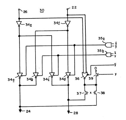
A schematic circuit for implementing the
four-state cell 30 of Figs. 2A-2D is shown in Fig.
3. The circuit comprises four tri-state inverters
34a-34d, two regular inverters 34e and 34f, two AND
gates 35a and 35b, a tri-state NOR gate 36 and three
transistor switches 37-39. The state of cell 30 is
controlled (i.e., programmed) by two bits, labelled
"x" and "y". Fig. 4 contains a self-explanatory
table listing the state of cell 30 as a function of
bits x and y. The tri-state inverters 34a-34d, the
tri-state NOR gate 36, and the transistor switches
37, 38 and 39 are turned on (i.e., closed) when the
applied control signal is high (i.e., a logical "1").
As previously stated, each cell or some cells
may need appropriate gain elements between its inpu.
and output connections in order to ensure that
logical wires function properly. Generally, pairs
of inverters are used for this purpose. To reduce
1287~22
C0440/7001WO
--19--
the number of inverters and thereby speed up the
circuit, adjacent cells may employ opposite logic
conventions on their inputs. That is, for a
particular cell a high input may correspond to a
logical "1", while for an adjacent cell a high input
may correspond to a logical "0". For ease of
reference these two types of cells may be referred
to as "red" cells and "black" cells since they are
arranged in the array similarly to the red and black
squares of a checkerboard. Fig. 5 illustrates the
resulting topology, with black cells 20-2 and 20-3
labelled "B" and red cells 20-1 and 20-4 labelled
"R". Figs. 6A - 6D depict the four states of the
"red" type of cell 40, while Figs. 7A - 7D depict
the corresponding states of the "black" type of cell
50. The red cells and black cells differ from the
basic cell 30 of Figs. 2A - 2D by the addition of
two inverters in each cell; in the red cells 40, the
inverters 41 are added in each output line of the
cell, whereas in the black cells 50, the inverters
51 are added on each input line of the cell. When
an inverter in the input circuit of a black cell is
connected to an inverter in the output circuit of a
red cell, the effects of the inverters cancel each
other, leaving the circuit the equivalent of that
which would be formed from the basic cell 30 of
Figs. 2A - 2D. For this reason, the inverters have
no effect on the logical operation of the array, and
the term "logical identity" as used herein refers to
the situation wherein an input line of a cell is
..... . ..
~. .
~2~371ZX
C0440/7001WO
-20-
connected directly to an output line of a cell as
well as the making of such a connection through an
inverter when opposite logic conventions are
employed on the inputs of adjacent cells.
Schematic circuit diagrams for red and black
cells 40 and 50, respectively, are contained in
Figs. 8 and 10. With reference to Fig. 8, red cell
40 is formed from four tri-state inverters 62, 64,
66 and 68; a tri-state OR gate 72; a pair of AND
gates 74 and 76; and three transistor switches 78,
82 and 84. The state of cell 40, like that of cell
30, is programmed by two bits, labelled "x" and
"y". Fig. 9 contains a self-explanatory table
listing the state of cell 40 as a function of x and
y, Correspondingly, Fig. 10 shows how a black cell
50 may be created from four tri-state inverters 92,
94, 96 and 98; a tri-state AND gate 102; a pair of
AND gates 104 and 106; and three transistor switches
108, 112 and 114. The state of cell 50 is also
-programmed by two bits, again labelled "x" and ~'y".
Fig. 11 provides a table listing the state of cell
50 as a function of bits x and y.
Since the term "cell" is used extensively
herein, it is important to appreciate that that term
has somewhat arbitrary boundaries, as Fig. 5
demonstrates. Thus, blocks of four cells may be
aggregated to form a regular structure having a
single type of "macro-cell" building block. Thus,
1~37~2X
C0440/7001WO
-21-
the group of cells 20-1, 20-2, 20-3 and 20-4 may be
considered the basic element of the structure, as
suggested by the dashed line 25 enclosing them. The
macro-cell enclosed by line 25 has both an input
connection and an output connection on each of its
north, south, east and west sides; and it can be
programmed to any of 256 states. Clearly this
approach may be extended in any dimension.
An array may also be built of cells of two
dist~nct types, which provide different logic
functions. This is to be contras~ed with the use of
red and black cells, which provide the same logic
functions and differ only in their electrical
implementations. However, even if two or more types
of cells are employed, it is still possible to
define a block, or macro-cell, such that the array
may be described as being built from such a single
type of block connected to its immediate neighbors.
A S__ nd Embodiment
Cells which make available more than four states
may also be employed. Figs. 12A - 12H depict one
possible set of states for an eight-state cell 120,
which is programmed by three bits x, y and z. Other
states (both in function and number) are, of course,
possible. Cell inputs are received on leads 123 and
125; outputs appear on leads 124 and 126. In Fig.
~ 287~2~
C0440/7001WO
-22~
12G, the logic element 122 is a Muller C-element:
this elemen~ is particularly useful in the
implementation of speed-independent logic. The
other states represented in Figs. 12A-12F and 12H
are self-explanatory, including outputs set to zero,
inputs wired directly to outputs tfor crossovers,
right-angle bends and fan-outs), and two-input OR
and NOR gates. Other states which might be of
interest include states containing flip-flops and
more complex circuits; the C-element might be
exchanged for a flip-flop, for example.
A schematic circuit diagram for the cell 120
appears in Fig. 13. This cell has five inverters
142A - 142E, a C-element 122, a NOR gate 146 and
fourteen transistor switches labelled 148A`- 148N.
The switches are programmable by three bits labelled
x, y and z. Fig. 14 provides a table listing a
mapping between bits x, y, and z and the various
cell states.
The Proqramminq System
In uS Patent 4,700,187, I described the essential of a
graphical system for programming an earlier form of
programmable logic cell and array which shares with
the present invention the basic concRpt of a
cellular arrangement of programmable logic units.
122
C0440/7001WO
23-
That programming system is also useful in connection
with the present invention and it has been enhanced
to provide the system designer with even more
powerful tools than were taught in the
aforementioned patent.
The programming system provides two design modes
to the user: (1) a circuit mode for creating the
lowest-level modules and ~2~ a block-diagram mode
for creating higher-level modules. In the circuit
mode, the user works directly with individual cells,
determining the function of each cell (which may
include, for example, a logic function or an
interconnection function).
Collections of cells may then be treated as a
block representing a functional module to be used in
the block-diagram mode. In the block-diagram mode,
the user does not deal directly with individual
cells or logic elements but, rather, with blocks
representing previously created modules. The size
and location of each block reflects ~he actual size
and location of the module in the array. Thus, a
block diagram on the screen of the graphics
programming terminal provides not only a functional
definition of the composite module, but also the
topological layout of the associated circuit.
In the block-diagram mode, the user is able to
create and manipulate a complex circuit by recalling
371ZZ
C0440/7001WO
-24-
previously created modules, moving modules, flipping
and rotating modules, duplicating modules,
interconnecting modules, and deleting modules and
interconnections. This ability to reorient modules
(and, therefore, circuits) without changing their
functionality facilitates the efficient
interconnection of functional blocks. Figs. 15A-15D
illustrate the progression from a logic diagram
(Fig. 15A) to a block representing the logic circuit
(Fig. 15B) to a module incorporating that circuit
(Fig. 15C), and thence to a higher-level block
representing that module (Fig. 15D). The techniques
for transforming modules by translation, rotation
and reflection (i.e., flipping) are developed below.
For purposes of the following discussion, it
will be assumed (to simplify the presentation) that
rectangular blocks are to be transformed. In
general, though, a "block" or "module" is any region
of the array, of arbitrary shape and size. A module
and its "origin" are considered to be "located" at
the position of its upper left corner cell (or the
equivalent, for non-rectangular modules), as a
convenient convention; other definitions can be used
just as easily, with appropriate modification of the
text which follows. Within a module, a cell is
located at coordinates (i,j), where the cell in the
upper left corner of the module is at coordinates
(1,1); "i" increases from left to right and "j"
increases from top to bottom.
, . ., , ~
128~1Z~
C0440/7001WO
-25-
Each module has a "vertical parity" and a
"horizontal parity"; these parities identify the
orientation of the inputs and outputs of the
module's cells. Parity will best be understood by
reference to Fig. 16. There, a module 152 appears
within dashed line 154. A module's horizontal
parity is determined by the direction of the
horizontally-directed output of each cell in the top
row of the module; with respect to module 152,
refer to output/input leads 156a-156f. Horizontal
parity is said to be "even" or "1" if the
horizontally-directed output from each cell in the
top row of the module is supplied to its eastern, or
right hand, neighbor. Conversely, a module's
horizontal parity is said to be "odd" or "0" if the
horizontally-directed output from each cell in the
top row of the module is supplied to the cell's
western, or left-hand, neighbor. Module 152 thus
has odd horizontal parity. Vertical parity is
treated in comparable fashion. A module's vertical
parity is said to be "even" or "1" if the
vertically-directed output from each cell in the
leftmost column of the module is supplied (e.g., see
leads 158a-158c) to the cell's southern, or lower,
neighbor. Conversely, a module's vertical parity is
said to be "odd" or "0" if the vertically-directed
output of each cell in the leftmost column of the
module is connected to its northern, or upper,
neighbor. Module 152 thus has even vertical parity.
12~712~
C0440/7001WO
-26-
A row or column may also be said to have parity,
with the same definitions being applied; thus, the
row or column may be thought of as a module which is
only one cell high or one cell wide.
To ensure that a transformed module has the
correct parities, an appropriate horizontal or
vertical translation of the module may be required
when a module is translated, rotated or reflected.
Note that translating a module by an odd number of
cells in the horizontal direction will cause a
reversal of the module's vertical parity and
translating the module by an odd number of cells in
the vertical direction will cause a reversal of the
module's horizontal parity.
For a simple translation of a module,
maintaining the correct parities in the transformed
modùle is accomplished by restricting movement to an
even number of cells in each direction. For
reflection and rotation, the situation is more
complicated and detailed procedures are given below.
The steps for reflecting a block about a
vertical axis are depicted in Fig. 17, which should
be read in relation to Figs. 18A and 18B. The
module shown in the dashed lines 170 in Fig. 18A is
to be reflected about its central vertical axis 172
(which bisects the module through its central
column, since the module is an odd number of columns
wide). Broadly speaking, reflection is accomplished
128~1ZZ
C0440/7001WO
-27-
by (1) establishing the position of the new,
transformed module in accordance with parity
requirements and (2) mapping the original cells onto
the cells of the new module. In detail, the
reflection proceeds as follows: First, the location
and dimension of the new module (i.e,, the module
resulting from the transformation) are initially
defined to be the same as those of the original
(i.e., untransformed) module (Step 192). Second,
the new module's location is offset (i.e., shifted)
by an odd number of cells vertically, to provide the
appropriate horizontal parity; typically, the offset
will be one cell in either direction (Step 194).
The module may also have to be shifted horizontally,
to achieve proper vertical parity; such a shift is
only required, however, if the new module spans an
even number of cells in the horizontal direction.
Such parity adjustment is necessary to ensure that
the new module contains the correct circuit. If
module parity is improper, the circu~t will not only
be reflected about the axis, but also the circuit
and its function will be altered. The parity
adjustment routine begins with a test to determine
whether the horizontal size of the module is even,
Step 196, and a horizontal shift is performed in
Step 198 if required. Having properly situated the
new module, each cell of the old module must be
mapped into the- space occupied by the new module.
In Step 202, a Pascal-type expression is given for a
procedure which accomplishes that operation. This
12~71~
C0440/7001WO
-28-
procedure comprises a pair of nested loops wherein
the new cell state assignments are calculated and
then replace the old cell state assignments. The
outer loop is indexed by the variable "j", which
denotes the vertical coordinate of a cell in the
new, reflected module, relative to the module's
origin (i.e., upper left hand corner). The
horizontal size of the new module (i.e., after
reflection), is represented by the variable
newModuleSize.h. The inner loop is indexed by the
variable "i", which denotes the horizontal
coordinate of a cell in the new module, relative to
the module's origin. The quantity "newCell[i,j]"
represents the state, or function, of the cell at
coordinates (i,j) in the new module; the quantity
"oIdCell[moduleSize.h-j+l,i]" represents the state
of the cell in the original, "old" module at the
indicated coordinates. The procedure of Step 202
first maps cell states of the old module into cell
states of the new module and then makes adjustments
in the new states, as required, to reflect its
reorientation. Some cell states retain their
identities through the transformation. The
adjustments of states for the new cells can be
performed through a look-up table or other
mechanism. Once the new cell states are known, the
corresponding bits in the cell state memory, which
control the programming of those cells, are set to
the appropriate values.
~871~
C0440/7001WO
-29-
The transformed module 170~ is shown in Fig.
18B, from which it will be appreciated that a
vertical translation was needed in order to achieve
proper parities. Cells 176, 178 and 182 have been
mapped to cells 176', 178' and 182'.
The steps for reflecting a block about a
horizontal axis are depicted in Fig. 19, which
should be read in conjunction with Figs. 20A and
20B. In Fig. 20A, a block originally shown at the
position of dashed line 220 is to be reflected about
horizontal axis 222. The reflection is performed as
follows: First, the location and dimensions of the
new module (i.e., the module resulting from the
transformation~ are initially defined to be the same
as those of the original (i.e., untransformed)
module (Step 242). Second, the new module's
location is offset (i.e., shifted) by an odd number
of cells horizontally, to provide the appropriate
vertical parity; typically, the offset will be one
cell in either direction (Step 244). The module may
also have to be shifted vertically, to achieve
proper horizontal parity; such a shift is only
required, however, if the new module spans an~even
number of cells in the vertical direc~ion. A test
for thls condition is performed in Step 246 and the
vertical shift is performed in Step 248 if
required. Having properly situated the new modules,
each cell of the old module must be mapped into the
space occupied by the new module. The procedure for
.
.
- .
:
,.
. .
.
~287~22
C0440/7001W0
-30-
doing so is performed at Step 252 and mirrors the
procedure in Step 202 of Fig. 17 for the reflection
about a vertical axis.
The transformed module 224 is shown in Fig. 20B,
with cells 226, 228, and 232 mapped on~o cells 226',
228' and 232', respectively. Note that both
vertical and horizontal shifting was required to
preserve vertical and horizontal parity.
A flow chart for accomplishing module rotation
is shown in Fig. 21. This flow chart should be read
in relation to Figs. 22-24. Fig. 22 shows a block
within dashed 'ine 260, prior to rotation. Fig. 23
shows the same block in its tentative new position
260' after rotation, prior to translation for parity
adjustment. Fig. 24 shows the block at its final
position 260" after rotation and translation.
The Fig. 21 procedure rotates a module by ninety
degrees in the counterclockwise direction. First,
the location and dimensions of the new module are
initialized (Step 270). This involves aligning the
cells at the upper left hand corners of the new
module and the old module and setting the horizontal
and vertical sizes of the new module equal to the
vertical and horizontal sizes, respectively, of the
old modul~. Next, the old module's horizontal
parity is compared with the old module's vertical
par1ty (Step 272). If the two parities are equal,
~28712~
C0440/7001WO
-31-
the location of the new module is offset
horizontally by an odd number of cells (Step 274).
Following that step, or following Step 272 if the
parities were unequal, a test is performed to
determine whether a vertical offset is required to
correct the horizontal parity of the new module
(Step 276). This latter step more specifically
involves comparing the horizontal parity of the old
module with the vertical parity of the rightmost
column of the old module. The rightmost column of
the old module becomes the topmost row of the new
module, so a comparison of their parities will
determine if the rotation will, without
compensation, produce the wrong horizontal parity in
the new module. If so, the parity is corrected by
offsetting the new module by an odd number of cells
in the vertical direction, Step 278. The function
[oldModuleParity.v XOR ODD(oldModuleSize.h-l)] in
Step 276 evaluates the parity of the column at
oldModuleSize.h-l, where oldModuleSize.h represents
the horizontal size of the old module, in numbers of
cells. The ODD function is TRUE when its argument
is odd and FALSE when its argument is even.
Performing the exclusive-OR operation (i.e., shown
as XOR in the drawing) on the vertical parity of the
old module and the function ODD(oldModuleSize.h-l)
yields the parity of the rightmost column of the old
module, which controls whether a vertical offset is
required in order to ensure that the new module will
have the proper horizontal parity.
128~ X
C0440/7001WO
-32-
Once the new module is properly positioned so as
to have the desired parity, each cell in the old
module's array must be moved to the proper location
in the new module's array. That is the function of
Step 280.
In the latter step, a Pascal-type expression is
given for a procedure which accomplishes that
operation. This procedure comprises a pair of
nested loops.. The outer loop is indexed by the
variable "i", which denotes the horizontal
coordinate of a cell in the new, rotated module,
relative to the module's origin (i.e,, upper left
hand corner). The horizontal size of he new module
(i.e., after rotation), is represented by the
variable newModuleSize.h. The inner loop is indexed
by the variable "j", which denotes the vertical
coordinate of a cell in the new module, relative to
the module's origin. The quantity "newCell[i,j]"
represents the state, or function, of the cell at
coordinates (i,j) in the new module; the quantity
"oldCell[oldmoduleSize.h-j+l,i]" rapresents the
state of the cell in the original, "old" module at
the indicated coordinates.
The flow charts of Figs. 17, 19 and 21 present
only the overall procedures used for reorienting
modules. In addition, various ministerial details
must be carried out in connection with the
12~37~22
C0440/7001WO
-33-
implementation of these procedures; for clarity of
explanation, these low-level details have not been
expressly discussed, as they will be readily
apparent to a skilled programmer.
In addition to implementing procedures for
rotating modules and reflecting modules about
horizontal and vertical axes, a graphics-based
programming environment for the array is capable of
allowing modules to be "dragged" across a display
screen (i.e., relocated on the medium by translation
of location) in the horizontal and vertical
directions. As this operation involves only a
simple translation of cell coordinates, its
implementation will be straightforward and requires
no further explanation.
Having thus described two exemplary embodiments
of the invention, it will be apparent that other
embodiments also may be created. It will further be
apparent that various alterations, modifications and
improvements will readily occur to those skilled in
the art. For example, other circuits may be used
for the cells and the cells may be assigned other
combinations of states. Additionally, cells may be
operatively connected to each other through
intermediate elements, such as switching elements
(which may also provide cross-overs, ninety-degree
bends and other wiring functions), in addition to
being directly connected. Such obvious alterations,
lZ~37~''2
C04~0/7001WO
-34-
modifications and improvements, though not expressly
described herein, are nevertheless intended to be
suggested by this disclosure and are within the true
spirit and scope of the invention. Accordingly, the
foregoing discussion is intended to be exemplary
only, and not limiting. The invention is limited
only as set forth in the following claims and
equivalents thereto.