Note: Descriptions are shown in the official language in which they were submitted.
~ ~ ~7 1~ 9
The present invention relates to a range determination
or ranging method using optical pulse signals transmitted by à
transmitter in the direction of a target and which are received
after reflection, converted into electrical signals and converted
in a signal processing means to a distance or range information.
The invention also relates to an apparatus for performing this
method.
Ranging methods are known which, in accordance with the
radar principle, use as aids pulsed electromagnetic signal so
that, with the knowledge of certain boundary conditions, it is
possible to determine the range by measuring the signal behaviour
between the target and the transmitter-receiver.
More sensitive ranging methods operating in the optical
frequency spectrum use solid state lasers (e.g. YAG, ruby or the
like) as transmitters. These lasers are optically pumped, the
range being determined by measuring the behaviour of an individ-
ual laser pulse with a correspondingly high energy. The electri-
cal efficiency of an optically pumped solid state laser is gener-
ally very poor due to the discharge lamps used for pumping. The
frequently necessary battery change is also disadvantageous in
operation. In order that an individual backscattered pulse has
sufficient energy to permit its detection, the energy of the
individual transmitted pulses must be very high. However,
pulses, whose energy exceeds a certain threshold value are pre~u-
dicial to the eyes, unless special safety measures are taken.
Semi-conductor lasers which, although allowing higher pulse
rates, e.g. lO to 100 kHz for GaAs have not hitherto been consid-
ered for ranging methods ln open terrain, i.e. at least over sev-
eral hundred metres, due to their relatively low peak output
power, which may not be exceeded for thermal reasons.
The present invention improves a ranging method and
apparatus of the aforementioned type, so that on the one hand
higher pulse rates than hitherto can be used for ranging purposes
-- 1 --
,.....
," ~
~ ~71q~3
and that on the other hand the signal strength of the received
signals is sufficient in order to permit completely satisfactory
signal processing and therefore ranging over the deslred range
with an adequate reliability level.
According to the invention there is provided a ranging
method between a transmitter-receiver for optical pulse signals
and a target, by the transmission of optical pulse signal groups,
the reception of the signals reflected by the target, converting
the received optical signals into electrical signals and then
processing the signals for deriving a measuring criterion, where-
in the transmitter directs pulse groups with a pulse rate in the
range between approximately 10 and approximately 150 kHz onto the
target, the reflected and received signal sequence is scanned
with a scanning frequency dependent on the transmission pulse
rate and digitized, the scan values obtained are continuously
added to the corresponding value for each individual transmission
pulse in the clock of the scanning frequency and the range infor-
mation is derived from the resulting signal. Suitably scanning
of the incoming signal sequence is performed with a scanning fre-
quency in the n~nosoaond range. Desirably the scanning of the
incoming signals is per~form~ed with a scanning frequency of
approximately ~ nun~eee*dG.
The present invention also provides an apparatus for
effecting said method which comprlses an analog-digital converter
supplied with the incoming signal and whose scanning frequency
can be controlled by a processor as a function of the pulse rate
of the transmission signal and downstream of said converter are
connected means for the parallel addition of the data supplied on
a parallel line from the analog-digital converter and the addend
signals of adder means processed in parallel form. Suitably
downstream of the analog-digital converter is connected a paral-
lel adder, whose output is connected across a shift register to
the input for the second addend of the parallel adder. Desirably
in the output line of parallel adder is provided a sensor for
7 ~4
indicating an overflow bit MSB to processor and in the parallel
connection between shift register and the input for the second
addend on parallel adder is provided a switch controlled by pro-
cessor and which, when an overflow bit MSB is lndicated by sen-
sor, downwardly displaces by one position the parallel signallines from the shift register to the parallel adder. Suitably
the processor is a microprocessor operating in the nanosecond
range and which contains the function of the transmission pulse-
related parallel adder.
The advantage of this solution is that, contrary to
original expectations, despite their low peak output powers, the
relatively inexpensive laser diodes which can be very adequately
controlled from the circuitry standpoint can be used for range
measurements over at least several hundred metres. This has sur-
prisingly led to considerable improvement in the sensitivity of
the measuring method by at least a power of ten, by typically by
several powers of ten, e.g. by a factor of 100. In addition,
equipment operating according to this method can be made very
small and have a light weight. The energy supply and control of
the laser diodes, as well as the subsequent signal processing can
be realized particularly simply, largely using standard compo-
nents. The higher electrical efficiency of a semi-conductor
laser compared with the hitherto used solid state lasers, as well
as the possibility of being able to operate with higher pulse
rates also constitute advantages.
Despite the lower peak power the inventive measure per-
mits larger ranges to be covered when measuring in a manner safe
for the eyes than when using individual pulsed lasers. Due to
the marked focusing of the laser beam, this method permits the
measurement of target distances with extremely high precision and
even without reflectors, i.e. without the prior fitting of
reflecting elements at the target.
Whereas hitherto scanning or sampling methods have been
~ 2~7~49
used in signal processing procedures for improving the resolution
of the signals received, i.e. for the better dlrect identifica-
tion thereof, the present method and/or apparatus aims at the use
of the sampling method for ~mproving the sensitivity of the
receiver and therefore for improving the wanted~spurious signal
ratio S/N.
The invention is described in greater detail here-
inafter relative to non-limitative embodiments and the accompany-
ing drawings, whereln:-
Fig. 1 is the block circuit diagram of a preferredembodiment for illustrating the method;
Fig. 2 is a time diagram for illustrating the method;
and
Fig. 3 is the block circuit diagram of a simplified
embodiment.
The principle of the inventive method essentially com-
prlses the use of the knowledge that the sensitivity of the mea-
suring method can be improved through the use of N pulses by a
factor of V N in accordance with information theory rules. It
has been found that through an optimum utilization of high pulse
rates, in accordance with such information theory rules it ls not
only posslble to overcome the disadvantages of the relatively low
admissible peak output powers for laser diodes, but in fact that
the measuring sensitivlty can be significantly improved, e.g. by
a factor of 100 compared with conventional methods.
Through the use of th0 scanning or sampling method on
the received pulse signal groups, it is possible to derive an
extremely precise decision criterion for the arriving again of
the pulses reflected by the target and therefore for the time
delay of the pulses between the time of transmission and the
- 3a -
~37'149
rearrival. Despite a low transmission energy relatlvely large
distances can be accurately measured in the case of a very good
S/N ratio.
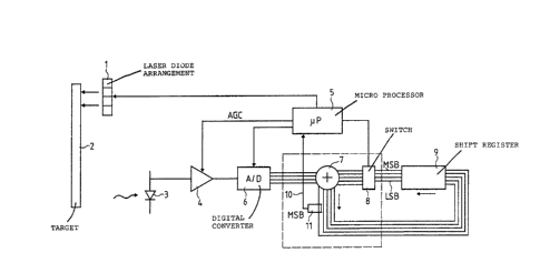
As is diagrammatically shown by Fig. 1, the pulse
sequence transmitted by a laser diode arrangement 1 is reflected
by a target 2 and then received by a light-sensitive cell, e.g.
an
- 3b -
,,
~ 2~37149
avalanche diode ~ preferably arranged in the transmitter
receiver. The~selected repetition frequency is e.g. in the
range 10 to ~g~ kHz. Pulsing is controlled and preferably
program-controlled by a micro processor 5.
The signals detected by the avalanche diode 3 are amplified
in an amplifier 4 to the extent necessary for the following
processing. In a following analog - digital converter 6, the
pulses received are digitized with a scanning frequency given
by the microprocessor 5. The clock of the scanning
operation is in the example 100 ns (nanoseconds). The
digitized data are e.g. transferred in the form of 4 or 6 bit
parallel signals to a parallel adder 7 and directly in the
clock of the a~forementioned scanning operation are added to
the corresponcling value for each individual pulse within a
scanning interval. This adding of the scan values of the
periodically t:ransmitted pulse sequences related in each case
to correspondLng scanning times leads to an increase in the
evaluated incoming signals and therefore to the indicated
rise in the s~ensitivity for the overall arrangement.
In order to obtain this action, in the represented example a
4 bit line from the analog - digital converter 6 is supplied
as a first adclend input to the parallel adder 7. The second
addend input of parallel adder 7 is in the form of a 5 bit
input and the adder output also has a 5 bit line. The
parallel line corresponding to the lowest point of the
parallel transmitted signal is designated LSB and that
associated with the highest point is designated MSB. A
sensor 11 is provided for establishing a bit signal appearing
on line MSB at the output of parallel adder 7 and is
connected across a MSB indicator line 10 to an input of
microprocessor 5. Microprocessor 5 establishes in
program-controlled manner whether a bit appearing on line MSB
is present during a complete scanning cycle between two
pulses transmitted by the laser diode arrangement 1.
The output of parallel adder 7 is connected to the input of a
7~49
--5--
shift reg:ister 9, in which there is a continuous intermediate
storage o:E the scanning cycle value supplied by parallel
adder 7.
A switch 8 controlled by microprocessor 5 is preferably
provided at the output of shift register 9 via a 4 bit
parallel lin.e. At the output side, switch 8 is connected via
a 5 bit parallbl line to the second addend input of parallel
adder 7. Thusr compared with its input, switch 8 has an
additional bit line on its output leading to the adder.
In the conn,ection between shift register 9 and switch 8,
according t:o fig 1 the lines for the lowest and highest
positions a,re once again designated LSB and MSB. The output
bit lines of switch 8 are switched up or down by one bit
position in. accordance with a criterion described hereinafter
and supplled by microprocessor 5, so that the association of
the incoming and outgoing bit lines is in each case displaced
by one position.
If an overflow signal from parallel adder 7 is detected on
the MSB indlcator line by microprocessor 5 and is maintained
over a complete scanning period, then microprocessor 5
supplies a switching signal to switch 8. The switch then
switched all its input lines to in each case an output line
lower by one place and remains throughout the next scanning
period in said position. Thus, during this time, the
previous MSB is now supplied as the second hiqhest bit to
parallel adder 7, the second highest as the third highest etc
and the information of the lowest position is not taken into
account during this time. All incoming bits during this
scanning period are therefore displaced downwards by one
pOSitiOIl by this measure.
Fig 2 diagrammatically illustrates the action of the
described signal processing on the received pulse signals I.
Whereàs signal line A shows the actual course of the signal
sequence received, line B represents the result of the signal
1~37~49
processing with the clearly raised scanning pulses. Such a
signal permits target acquisition and therefore reliable
ranging with a roughly 100 times better sensitivity when
using 10,000 pulses compared with a known method using a
threshold value detection within a given pulse window.
As a result of the selected, completely parallel siqnal
processing, there is a very high processing rate for the
pulses received from the avalanche diode. There is a
correspondingly high resolution or sensitivity of the means
for relatively weak pulse signals of the laser diodes
received over a greater distance. As a variant of the
previously described embodiment, the parallel adder 7
represented in fig 1 as a discrete component can be
integrated into microprocessor 5. When using a
correspondingly fast microprocessor 5, it is even possible to
obviate the use of a discrete shift register 9 and its
function can then be performed by the processor.
Fig 3 shows a simplified exemplified variant, in which a
microprocessor 20 with parallel adder integrated therein is
used for direct signal processing. Preferably this function
is fulfilled by very fast signal processors, whose operating
frequency is in the nanosecond range. The functions
described for the first embodiment according to fig 1 are
realized by corresponding programming of processor 20. As
the processing principle has already been described, details
of a corresponding program are not explained here. As in
the embodiment according to fig 1, here again a gain control
signal AGC for amplifier 4 can be derived from microprocessor
20.
Apart from the indicated embodiments, other solutions
realised by programming or circuitry are possible, which make
use of the same, previously described method features, in
order to obtain a usable criterion for ranging from
relatively weak incoming signals.
. .