Note: Descriptions are shown in the official language in which they were submitted.
3~ ~
1~69-004
BAC~GROUND OF TEIE INVENTION
1. Field of the Invention
The present invention relates to a controlled-output
amplifier whose output power may be set to any of a number
of predetermined levels. More specifically, it relates to a
controllable-gain amplifier whose output is controlled by a
servo loop that includes a half-wave rectifier ~or sensing
the output power and whose gain is controllable to maintain
a desired power level over a wide ran~e of amhient
temperature.
2. Discussion of the Prior Art
Controlled-output amplifiers known in the prior art
include a controllable-gain amplifier stage connected in a
servo or feedback loop in which the output power is sensed
and compared with a reference. The resulting difference or
error signal is used to control the gain of the amplifier
stage, thereby maintaining the amplifier output at the
desired power level. Power sensing is usually accomplished
by a diode, frequently referred to as a "detector diode,"
which is connected to a capacitor to form a half-wave
rectifier. However, diodes possess certain characteristics
~L
,.~,,",,,~.~
~' ' : ':'' '
.
28~384 `
R69-004
which may produce adverse effects in some application~.
First, if the monitored power levels are relatively low
~e.g. on the order of tens of milliwatts or less), the
forward voltage drop of the detector diode is large in
comparison to the rectified signal and variations in the
forward drop may therefore introduce significant errors into
the rectified signal.
Unfortunately, the forward voltage drop of a diode is
highly temperature dependent. For silicon diodes, the
forward drop typically varies on the order of -2mV/C. In
addition, the rate of change of the forward drop with
respect to temperature is dependent on the bias current
flowing through the diode. Thus, over a wide ambient
temperature range, the forward voltage drop will vary
significantly.
Third, diodes typically provide very limited dynamic
ranges. In other words, a diode can sense signals only
within a narrow amplitude range without being driven into
saturation. In applications where the sensed ~ignal may
vary by an order of magnitude or more, the diode may
saturate, thereby lntroducing errors into the rectified
signal.
A conventional solution for minimizing the problems
--3--
~. ",
......
. . .... ., .. ... .; . . . ~ .. ,~....... . . .. .: , .. ...... .. . . ...... . ... .
.
' ~L2~73~3~
R69-004
with forward voltage drop and drift described above i~ the
application of temperature compensation to the detector
diode. In one form of compensation, a "compensation diode"
i6 connected 60 that its forward drop biases the detector
diode at the threshhold of conduction and thus effectively
cancels the forward voltage drop of the detector diode.
Assuming that the two diodes have "matched" temperature
characteristics, their forward voltage drops will
substantially track each other as the temperature varies ~nd
the detector diode will thereby remained biased at the
threshhold of conduction.
There are several disadvantages associated with this
type Df temperature compensation. First, the detector and
compensation diodes must have nearly identical temperature
characteristics to ensure close tracking between their
forward voltage drops. Such matched diodes are relatively
expensive components; typically they must be tested for
close matching before they can be assembled in a desired
circuit. Second, the two diodes must be located in close
thermal proximity to each other in order to minimize any
difference in ambient temperature. If a significant
temperature difference exists, the forward voltage drops of
the two diodes will not be the same and the forward voltage
--4--
`
. '
: , ' .
,
lZ~7~84t `~
~ 69-004
drop of the detector diode will not be effectively cancelled
as the temperature varies, resulting in temperature-related
variations in the output of the detector diode.
SUI~MARY OF THE INVENTION
The present invention provides a controlled~-output
amplifler whose output power may be set to one of a number
of predetermined levels and maintained substantially
constant over a wide ambient temperature range. The
amplifier comprises a detector which senses the output power
of a controllable-gain amplifier ~tage and produces a half-
wave rectified signal in response thereto. The detector
includes a diode which may be biased to one of a number of
preselected states by a bias control unit. Thus, when the
controlled-output amplifier is operating at relatively low
power levels, the diode is biased with a relatively small
current. The result is that the diode has a high impedance
and a large proportion of the sensed signal appears across
the diode. Thus, the diode is configured for maximum
sensitivity for sensing the relatively small signals.
Alternatively, if the controllsd-output amplifier is
operating at relatively high power levels, the bias current
~. ~
3~3~
6~ 40~
o~ the diode is increased, thereby reducing ~he impedance of the
diocle. As a result, a lesser proportlon of the sensed signal
appears across the diode, which tends to prevent the diode from
being driven into saturation.
By virtue of these multiple bias "sta~es"~ ~he detector
displays a wide dynamic range ard is capable of accurately sensing
signals which may vary hy an order of magnitude or more. Because
the bias control unit establishes the corxect bias state of the
dlocle regardless of the ambient temperature, there is no need for
a conventional compensation diode. Thus, a siynificant cost
savinys may ~e reali~ed by the elimination of both the
compensatiorl diode and the accompanying pre-installation testing
which is normally required for matched diodes.
In summary, the present invention provides a controlled-
output amplifier having an input and an output, said input for
receivi.ng a preselected input signal, said output for producing an
output signal having a substantially constant predetermined
magnitude, said amplifier comprlsing: controllable-~Jain amplifier
means having first and second inputs and an output, said first
input adapted to receive said preselected input signal, said
second input adapted to recelve a gain con~rol signal, said output
providincJ the output slgnal of said controlled-outpllt amplifier;
rectlfier means having an :lnput and an output, said input coupled
to the output of said controllable-gain anlplifier means, said
rectiEier means producing at said output a signa~ indicative of
the magnitude of the output signal of sai.d controlled-ou~put
amplifier; bias control means having an input and an output, said
.: ~
~ !
'
' ' '
73~'~
64~ 40~
input adapted to receive a bias con~rol siynal, .said output
coupled to the rect.ifier meansr said control means biasiny said
reetifier means in one of a plurality of predetermined bias ~tates
in response to said bias control signal; comparison means having
flrst and second inputs and an output, said first input couple~ to
the output of said rectifier means, said second input adapted to
.receive a re~erence signal r said comparison means producing a
signal at said output which is indi.cative of the dif-ference in
magnltude of the reference signal and the signal produced at the
output of said rectifier ~eans; and con~rol signal generator means
having an inpu~ and an output, said inpu~ coupled to the output of
said comparison means~ said output coupled to the second input o~
the controllable-gain amplifier meansr said generator means
producing th~ gain control signal in response to the signal
produced at the output of the comparison means r whereby the gain
of the controllable-yain amplifier means is adjusted so as to
maintain the output signal of the controlled-output amplifier, at
the predetermined magnitude.
BRIEF DESCRIPTION 0~ THE DRAWINGS
This invention is polnted out with particularity in the
appended claims~ The above and further advantayes of this
invention may be better understood by referring to the followlng
descripkion ta]cen in conjunc~ion with the accompanying drawinqs,
ln which:
Fiyure 1 is a block diagram of a controlled-output
6a
,,.~
.~
7~
~ 6~-004
amplifier known in the prior art;
Figure 2 is a block diagram of a controlled-output
~mplifer constructed in accordance with the preferred
embodiment of the present invention; and
Figure 3 is a detailed circuit diagram of the detector
shown in Figure 2.
DETAILED DESCRIPTION OF AN ILLUSTRATIYE EME~ODIMENT
Figure 1 is a block diagram of a controlled-output
amplifier 10 known in the prior art. The amplifier 10
includes a feedback or servo loop which operates to maintain
the output power at a substantially constant, prede~ermined
level. An input signal Ei is received at an input terminal
12 of a controllable-gain amplifier 2. An output signal E
is provided at an output terminal 14 of the amplifier 2. An
input terminal 16 of a detector 4 is connected to the output
terminal 14. An output terminal 18 of the detector 4 is
connected to an inverting input terminal of a comparator 6.
A re.~erence signal V f is provided to a non-inverting input
tecminal o~ the comparator 6. An output terminal 20 of the
comparator 6 is connected to a control signal generator 8.
Finally, an output terminal 22 of the control signal
'
~:!373~3~
R69-004
generator 8 is connected to the controllable-gain amplifier
2.
The detector 4 typically includes a half-wave
rectifier, which produces a rectified ~DC) signal at output
terminal 18 that is indicative of the magnitude of E . The
comparator 6 in turn compares the rectified signal with the
reference signal V ~ and produces an error signal at output
terminal 20 which is indicative of the difference in
magnitude of these input signals. In response, the control
signal generator B psoduces a signal at output terminal 22
which causes the gain of the amplifier 2 to either increase
or decrease so as to reduce the error signal. In this
manner, the output power of the amplifier 10 is maintained
at a substantially constant level. Additional conventional
circuitry (no~ shown) may be included to provide a plurality
of reference signals similar to V f, thereby permitting the
amplifier 10 to operate at any of a number of predetermined
power levels.
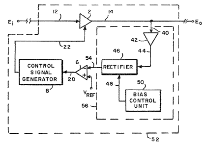
Figure 2 is a block diagram of a controlled~output
amplifer 52 constructed in accordance with the preferred
embodiment of the present invention. For simplicity,
components, terminals and signals which are similar to those
shown in Figure 1 retain the same reference numerals~ A
.
.
',
:.' ' ,
~ :~Z1~3~
R69-004
detector 56 comprises an amplifier 42, a rectifier 46 and a
bias control unit 50. An input terminal 40 of the ampli~ier
42 i~ connected to the output terminal 14. ~n output
terminal 44 of the amplifier 42 is connected to the
rectifier 46. An output terminal 48 of the bias control
unit 50 is also connected to the rectifier 46 to establish a
predetermined bias current through the rectifier. An output
terminal 54 of the rectifier 46 is connected to the
inverting input terminal of the comparator 6. The remaining
components and connections are similar to those shown in
Figure 1.
Figure 3 is a detailed circuit diagram of the detector
56 shown in Figure 2. Referring now to Figures 2 and 3, the
amplifier 42 comprises a transistor 68 in combination with
resistors 60, 64, 66 and 70. A coupling capacitor ~8,
connected to the base of the transistor 68, couples the
amplifier 42 to the input terminal 40. A source of supply~
voltage V provides a DC bias voltage to the transistor 68.
~ he rectifier 46 comprises a detector diode 102, a
capacitor 104, and a resistor 110 connected in a half-wave
rectifier configuration. The collector of the tranfiistor 68
iB coupled to the rectifier 46 by a coupling capacitor 72
and a resistor 76. The output of the rectifier 46 in turn
' : '
' ' ,
~ ~LZ~73~ `
~ 69-004
ifi coupled to an invertin~ input terminal of a comparator
130 by a resistor 120~
The bias control unit 50 compsises transi~tors 86, 90,
100 and 112, related capacitors and resistors, and the
c~mparator 130 as indicated in Figure 4. A source of
control voltage V is provided to the base of the transistor
86 through a resistor 84.
The operation of the bias control unit 50 may be
summarized as follows. First, assume that the control
voltage V is sufficiently high that transistor 86 is turned
on, thereby turning off transistors 100 and 112 ~nd thus
turning off transistor 90. In this bias state, the DC bias
path for the detector diode 102 extends from the supply
voltage V , through the resistor 82, through the diode 102
and through the resistor 110 to ground. Using the
components and nominal values listed below in the Table of
Components, the detector diode 102 will receive a bias
current of approximately 25uA and will therefore have a high
impedance relative to the output impedance of the amplifier
42. Accordingly, a large proportion of the signal voltage
received from the amplifier 42 will appear across the diode
102. Thus, the diode will exhibit a relatively high
detection sensitivity, which is desirable for sensing
_,ln.-
. .
`~
,~i
3 ~:8~38~
R69--004signals of relatively small magnitudes (e.g. on the order of
approximately -12 dsm to 2 dBm).
As described above, the forward voltage drop of the
detector diode 102 will vary in response to changes in the
ambient temperature. However, due to the relatively small
~ias current, the effect of any change in the for~ard
voltage drop due to temperature is minimized by the
increased sensitivity such that over a range of
approximately -35C to 80C, the output power level of the
controlled-output amplifier 52 may be maintained within 2
d~m of the predetermined level. In this bias state, the
detector diode 102 is optimally configured, both in terms of
sensitivity and temperature stability, for sensing signals
of relatively small magnitudes without the use of a matched
compensation diode. The pre-installation testing normally
required for such matched diodes is also advantageously
eliminated.
Now assume that the control voltage V is decreased
sufficiently to turn off transistor 86, thereby turning on
transistors 90, 100 and 112. A bias current of
appcoximately 8mA now flows through the detector diode 102
and the small-signal impedance of the diode is reduced ti.e.
to the order of 50 ohms). The decreased impedance of the
_~ I
. . ; l; ,. :
' '.
' ~
373~3~
Rb~-004
detector diode 102 attenuates signals received from the
amplifier 42, which prevents the diode from being driven
into 6aturation by signals of large~ magnitude (e.g. on the
order of approximately 2 dBm to 12 dBm)O
Again, the forward voltage drop of the detector diode
102 will vary in response to changes in the alnbient
temperature. Also, due to the larger bias current, the rate
of change of the forward drop with respect to temperature
will increase. However, since the magnitudes of the sensed
signals are larger, the change in the forward drop of the
diode is still small by comparison, and the output power
level of the controlled-output amplifier 52 may still be
maintained within + 2 dBm of the predetermined level over
the same ambient temperature range as above.
It should be apparent to those having ordinary skill in
the art that any number of preselected bias states may be
provided to meet the requirements of a particular
application.
The following Table of Components identifies components
and nominal values for the detector 56 shown in Figure 3.
.
~69-~04
~ABLE OF COMPONENTS
Reference Number Component Number or Nominal Value
V BVDC
58 33pF
1 kilo-ohm
62 33pF
64 4 kilo-ohms
66 10 ohms
68 NE85634
7~ 47 ohms
72 33pF
74 .01uF
76 4.7 ohms
78 470 ohms
33pF
82 lS0 kilo-ohms
84 10 kilo-ohms
~6 MM~2222
88 4 kilo-ohms
MMBT2907
~ 92 680 ohms
iJ
: .,
- ' ,'' ' '
:' ~', ;, ' , ' , '
1~73~
R69 - 004
100 MMBT2222
102 1 SSg7
104 33pF
106 4 kilo-ohms
108 4 kilo-ohms
110 150 kilo-ohms
112 MMBT2222
114 680 ohms
116 33pF
118 . OluF
120 1 kilo-ohm
122 lO kilo-ohms
124 68 kilo-ohms
126 6800pF
128 8 kilo-ohms
130 LM2902
The foregoing description has been limited to a
specific embodiment of this invention. It will be apparent,
however, that variations and modifications may be made to :
the invention, with the attainment of some or all of the
advantages of the invention. Therefore, it is the object of
~ the appended claims to cover all such variations and
,, ~
. ~ . , .
. .
.
'
;, ' : .
` ~Z8~3~4
6~421-~5
modi.fications as come within the true spirit and scope of the
invention.
,