Note: Descriptions are shown in the official language in which they were submitted.
7~)8
~OR-CO~ECTING BIT-SE~IAL 3ECODER
BACKGROUND OF THE INVENTION:
This invention relates to an error-¢o.rrectin~ decoder
for use as a counterpart of an error-correction encoder,
In the manner which will later be describecl more in
detail, an error-correction encoder is for use in encoding an
information symbol sequence into a code symbol sequence which
comprises the information symbol sequence and a redundancy bit
sequence in aeeordanee with a predetarmined rule, The oode symbol
sequence is either transmitted to a transmission channel or route
or stored in a storage medium,
Eithar transmitted through the transmission channel
or reproduced from the storage medium, the code symbol sequence
is supplied to a counterpart errOr-corrQcting decoder as an input
code sequence, When compared with the code symbol SeqUQnce produced
by the encoder, the~input eode sequence may have an error or
errors mainly due either to noise in the transmission channel
or to physical defects of the storage medium. Regardless of
presence and absenee of sueh an error, it is possible to understand
that the input eode sequenee eorresponds to the eode symbol sequence,
The redundaney bit sequence is used in the decoder ~n automatically
eorreeting the eror or errors. Correeting the error or errors,
the decoderdecodes the input eode sequence into a decoded symbol
sequence which gives a reproduction of the information symbol
sequence.
'~. . '
~2a740~
~.
It will also be described more in detail later in the
J followinæ that a conventional error-correcting decoder comprisss
an encoder repllca responsive to the input cods sequen¢e for
producing a repllca output signal with reference to the predete~mined
rule and a sequential decode oontroller for exeoutlng a sequential
decodlng algorlthm on the lnput aode sequence and the replica
output signal to produce a control signal, Controlled by the
control signal, the encoder replica decodes the input code sequence
lnto the above-mentloned decoded symbol sequence,
The sequential decoding algorithm has been executed
on the input code sequence and the replica outpus signal on a
symbol by symbol or code by code basis, It has now been confirmed
as will become clear as the description proceeds that the prior
art error-correcting decoder has a slo~ decoding speed as a result
of execution of the sequential deooding algorithm on such a symbol
by ,symbol basis when each information symbol of the information
symbol sequence has a long bit or symbol length, On the other
- hand, it is highly desirable to deal with a great amount of data
or information at a high speed with no error in the present-day
information-intensive social system which is realiæed by a combination
of electrical and/or optical communication systems and electronlc
digital computers,
SUMMARY OF THE INV~NTION~
It is therefore an object of the present invention
to provide an error-correcting decoder which has a high decoding
speed even for an input code sequence wherein each information
symbol has a long bit length,
37~08
It is another object of thls invention to provlde an
error-correcting decoder of the type described, which co~prisss
an encoder replica and processes an output signal of the encoder
replica on a bit by bit basis, that is, which is operable as
an error-correcting bit-serlal decoder,
Other ob~ects o~ thls lnventlon will beoome clear as
the description proceeds,
It is possible on describing the gist of this invention
to define that an error-correcting decoder to whlch this invention
is applicable, is for use as a counterpart of an error-correction
encoder for encoding an information symbGl sequence into a code
symbol sequence comprising the information symbol sequence and
a redundancy bit sequence in accordance with a predetermined
rule and comprises (1) an encoder replica responsive to an input
code sequence corresponding to the code symbol sequence for producLng
a replica output slgnal with reference to the predetermined rule
and ~2) a sequential decode controller for executing a sequential
decoding algorithm on the input code sequence and the replica
output signal to supply the encoder replica ~ith a control signal
for use in making the encoder replica decode the input code sequence
into a decoded symbol sequence ~hich gives a reproduction of
the information symbol sequence.
Accordlng to this invention, the above-defined decoder
is characterised in that the encoder replica comprises (A) a
one-bit memory, (B) input means for delivering consecutive bits
of the input code sequence to the one-bit memory to make th~
one-bit memory successively memorize the consecutive bits, and
- (C) output means for producing replica output bits in response
FROII PRTENT5 ~I~JISION,NE~ 7~ 3i~ a4~ IS PRIJE :~
'Z,.
4~3
to the consecutive blt~ succeesively memoxi~ed ln the one-bi*
memory and for dellv~rlng the replica output bits in bit eeries
to the sequentlal decode oontroller as the repllca output slgnal
produoed with referenoe to the predetermined rule 80 tha~ the
enooder replloa may bo respon~ive to the oontrol si~nal to pro~uoe
the decoded ~ymbol sequence in response to the conseolltlv3 blts
sucoessively memoxized ln the one-bit memory.
Preferably, the deooder further oomprl~e~ (i) blt positlon
counting mean~ respon~ive to the control slgnal for counting
positions of the respective oonsecutive blts ln the ~nput code
sequence to produce a blt position count ~ignal representativs
of the positions and (il) a discriminator re~ponslve to the bit
position ¢ount slgnal for produoing a first and a second disorimina-
tlon signal whereln the first dlsorimination si~nal indioates
positions of span blts colleotively oorrespondlng ln the input
aode sequence to the information symbol seguence and wherein
the second discrimination 3ignal indicate3 positions of interml-ttent
bits collectlvely oorrespond1ng in the ~nput code sequence to
the redundancy ~lt ~equence, In thi~ event, the output means
comprises a replica output selector responsive to the fir~t discrimina-
tlon slgnal for selecting, as tentatively predioted bits, the
oonsecutlv~ bits successively me~ori~ed in the one-bit ~emory
and responqive to the second discrimination signal for selectin~,
as parlty bies, the output bits of a function generator
25 to deliver the tentatively predic~ed blts .
and the dummy blt~ in bit serle~ to the sequential decode aontroller
as the replica output bits,
-- ,
- \
7408
According to an aspect of thls in~ention, thc bit position
counting means comprises a position counter responsive to the
control signal for counting the positions of the res~ective consecuti~e
blts in the lnput code sequence to produce -the bit position count
signal,
According to another aspect of this invention, the
bit positlon counting means comprises (a) ~.po~it~ion co~n.ter
responslve to the control signal for counting the positions of
the.respectl~e consecutive bits in the input code sequence to
producs a subsidiary position count signal representative of
the positions of the respective consecutive bits, (b) synchronism
shift counting means responsiYe to the control signal for counting
an amount of shift in synchronism of the input code sequence
to produce a synchronism shift count signal representative of
the amount of shift, and (c) a correction circuit responsi~e
to the subsidiary position count signal and the synchronism shift
count signal for correcting the subsidiary position count into
the bit position count in response to the amount of shift to
produce the bit position count signal.
BRIEF DE9CRIPTION OF THE DRAWING:
Fig, 1 shows a block diagram of a specific example
of error-correction encoders for use in facilitating an understanding
of the instant invention;
Fig, 2 shows a block diagram of a more general example
of the error-correction encoders for a similar use;
Fig, 3 is a block diagram of an error-correct~ng decoder
according to a first specific embodiment of this invention;
F ~ O II P R T E N T S D I ~ S I I~ N, I~I E C I g ~ 7 ~ ':J rJ l ~ 4 ~ b l 'J r ~
7~08
Fis, ~ iq A blook diagram of an error-correoting de¢oder
ao¢ording to a first more general embodiment of thi~ lnvontion~
Fi~ 5 15 a block dlaer~m of an error-corr~cting deooder
aooording to a second ~peoi~lo ombodlment o~ ~hi~ lnvontlon
and
Fig, 6 is a block diagram of an arror-corre¢tlng decoder
aooording to a seoond more general embod~ment of thls l~ve~tion,
DESC~IPTION OF THE PREFERRED EMBODIMENT~
~ eferring to Fig, 1, a speoifi¢ example o~ error-corre¢tion
enooder~ will be desoribed at first in ordar to ~acllitate an
under~tanding of the present invention, Such an error-coxrection
encodar wlll briefly be called an encoder in~ofar a~ no lnoonYenience
arises,
In Flg, 1, the encoder has encoder input and output
ter~inal~q 21 and 22. The ancoder outp~t terminal 22 ls for ¢on~ection
to either a txansmission ohannel or xoute or to a storage medium
: (not shown), It will be assumed for a short while that the output
term~nal 22 ls connected to a transmission channel,
The enooder input terminal 21 i supplied Nith a sequence
of information bits representatlve of data or information which
should be transmitted to the transmlssiQn channel to~ether wlth .
a ~equenoe of redundancy blts, For thi~ purpose, the information
blt sequenoe is delivered from the input terminal 21 to a se~ial-~o-
~arallel converter 23 whioh is ~or segmentlng the informatlon
blt ~equence into a sequenoe of information symbol~ having a
oommon blt or symbol length of three blts and i~ for producing
the bits of each information symbol in bit parallel at a tim~.
,
F R Q M F~ R T E N T S D l V l S l O N ~ N E ~ , 7 i~ u ~ J l ':~ d~ J :'LI ,~ l .J , ,, .~
'.~ C~.
l~:r~'740~3
The encoder compri~es an ano~der state holdi.ng oircult
2~ which, ln turn, oomprises flrst through thlrd parallel shi~t
registers 26, 27, and 28 depioted ln A staggered fa~hlon merely
for oonvenienoe o~ lllustration, In the ex~mpls b*ln~ lllust~atcd,
each shift reglstex has ~ir~-t -through thlrd ~tage~ f~om a le~t
end to a right end o~ that ~hiYt register, The first stage~
of the respeotive shift reglster6 26 through 28 are conneoted
to the serie~-to-parallel conYerter 23 to rece~Ye parallel bits
of each informat~on symbol from the serles-to-paxallel converter
23, Inasmuch a~ each shift register has three stages, such parallel
bits of three informatlon symbol~ are held in the state holdin~
oircult 25 at a time ~nd are shifted through the respective shift
register~ 26 to 28 r~ghtwardly of the figure in the ~anner known
in the art. In this manner, the state holding circuit 25 has
an en¢oder lnternal ~tate which is renewed when suppl~ed ~ith
each informatlon symbol from the erie6-to~parallel converter
23 a~ a fresh lnformation symbol At this instant o~ t~me, the
state holding circuit 25 produces, as an output information symbol~
in bit parallel, one of the three information symbols that ~ held
20 in the l~ft end~ of the respecti~e shift registers 26 to 28,
The encoder further comprise~ an encoder function generator
29 coupled to the encoder ~tate holding circuit 25 in a predetermined
manner which will presently be exempl~fied, Re~pon6ive to the
enooder internal ~tate of the ~ta~e holding oircuit 25, the function
generator 29 produces one or a plurality of redundancy bits concurrent-
ly with production in bit parallel of each output information
oyrbol fro~ the ~tate holdin~ oirouit 25
~2~37408
In Fig. 1, the encoder function generator 29 comprises
first through sixth Exclusive OR circuits 31, 32, 33, 34, 35~
and 36, Supplied with the bits which are kept in the respective
first stages of the first and the second shift registers 26 and
27, the circuit 31 produces a ~irst output bit, Sup~lled with
the bits from the second stage of the first shift re~Lster 26
and from the first stage of the third shift register 28, the
circuit 3Z produces a second output bit, Supplied with the bits
~rom the respective third stages of the second and the third
shift registes 27 and 28, the circuit 33 produces a third output
bit, Responsive to the flrst and the second output bits, the
circuit 34 produces a fourth output bit. Supplied with the third
output bit and ~ith the bit from the second stage of the third
shift register 28, the circuit 35 produces a:.fifth ou~put bit,
The third stage of the first shift register 26 and the second
stage of the second shift register 27 are connected ~o none of
the circuits 31 through 36, Responsive to the fourth and the
fifth output bits, the circuit 36 produces an odd par-ty bit
as each redundancy bit of the redundancy bit sequence,
20 From the encoder state holding circuit 25 and the encoder
function generator 29, the output information symbol and the
redundancy bit are delivered to a parallel-to-series converter
39 as four parallel bits of a code symbol. For transmission
to the transmission channel, the parallel-to-series converter
2~ 39 delivers the bits of a sequence of such u~cde s~mbols to the
encoder output terminal 22 in bit series, In this manner, the
code symbol sequence comprises the information symbol sequence
and the redundancy bit sequence in accordance with a predetermined
. , ~.
;,'., "'~ :
; ` ~ `' ,' `'
3'74~)~
rule.
For a different rule, the encoder function
generator 29 may be coupled in a di~ferent manner to the
encoder state holding circuit 25. Each shift register may
have a different number of stages. The parallel-to-s~ries
converter 39 may differently convert the parallel bits of
each output information symbol and each redundancy bit into
series bits of the code symbol.
Turning to Figure 2, a more general example of the
encoders comprises similar parts which are designated by
like reference numerals and are operable with likely named
signals. In the example being illustrated, the encoder is
for code symbols of a common bit length of n bits in which
a singla redundancy bit is added to each information symbol
having a bit length of ~n - 1) bits.
The 3 series-to-parallel converter 23 produces
parallel bits, (n - 1) in number, of each information
symbol at a time. The encoder state holding circuit 25
comprises (n - 1) parallel shift registers like the state
holding circuit 25 described in conjunction with Figure 1.
When each information symbol is delivered from the series-
to~parallel converter 23 to the left ends of the respective
shift registers in bit parallel as a fresh information
symbol, the output information symbol is produced also in
bit parallel from the left ends of the respective shift
registers and is delivered to the parallel-to-series
converter 39. The state holding circuit 25 has an encoder
internal state which is renewed when supplied with each
fresh information symbol to produce the output information
symbol. The right ends of the (n - 1) shift registers are
depicted at the top thereof.
- . .
~3'7~0~3
The encoder function generator 29 is couple~ to the
encoder state holdlng circuit 25 in a predeterm~ned manner to
receive ~n - 1) bits of each information symbol from the respective
shift registers. Depsnding on -the predetermined manner of couplin~,
the function generator 29 dellvers one or a plurality of redundancy
bits to the parallel~to-series converter 39 simultaneously with
delivery of (n - 1) parallel bits of each output information
symbol from the respective shift registers to the parallel-to-series
converter 39. In Fig. 2, only one redundancy bit is produced
at each tlme instant. In any event, a code symbol se~uence is
transmitted in bit series to the transmission channel through
the encoder output terminal 22.
Reviewing Figs. 1 and 2, it will be understood that
the encoder function generator 29 is for producing a redundancy
; 15 bit sequence in response to the encoder internal state which
the.encoder state holding circuit 25 has and which is successively
renewed by an informatlon symbol sequence The encoder is therefore
for use in encoding an information symbol sequence into a code
symbol sequence which comprises the information symbol sequence
20 and a redundancy bit sequence in:.accordance with a predetermined
rule. Incidentally, a multilevel modulator may be substituted
for the parallel-to-series converter 39 when the encoder output
terminal 22 is connected to a transmission channel.
In the manner written by George C. Clark, Jr., and
J. Bibb Cain in a book titled "Error-Correction aoding for Digital
Communications" which was first published 1981 by Plenum Press,
New York and London, particularly on pages 227 through 231 of
the book~ various codes are used in error-correction encoding~
t
., . "~'''''' ,.
12~ 0~3
11
~y way of example, the code symbol may be a tre0 code, such as
a convolutional code or a trellis code, From a different point
of view, ths code symbol may bs a systematic code which is formed
by ad~ition of a predetermined number of redundancy blts to ea¢h
information symbol, The predetermined number may be equal to
unity as exemplified above in connection with the specific and
the more general examples of the encoders, Al-ternatively, the
code symbol may be a nonsystematic code which is other than the
systematic codes like a quick look-in code. It should be noted
here that the systematic ccde is commercially important among
the tree codes of various types,
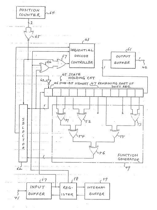
Referring now to Fig, 3, the description will proceed
to an error-correcting decoder according to a first specific
embodiment of this invention. Like the error-correction encoders,
such an error-correcting decoder will simply be called a decoder,
It will be assumed that the decoder being illustrated is for
use as a counterpart of the encoder illustrated with reference
to Fig, 1. That is, the decoder is for use in combination ~ith
an encoder which encodes three-bit information symbols into a
four-bit code symbol sequence with a single redundancy bit added
to each information symbol in accordance with a predetermined
rule exemplified in conjunction with Fig, 1,
The decoder has decoder input and output terminals
41 and 42, In the manner which will become clear as the description
proceeds, the decoder comprises an encoder replica and a sequential
decode controller 43, In Fig, 3, the encoder replica comprises
a decoder state holding circuit 45 whlch is implemented by a
single shift register consisting of a one-bit memory 46 at a
~2~3'7a~08
12
left end as a first stage of the shift register and second and
other consecu-tively numbered stages as a remaining part 47,
The encoder replica further comprises a decoder function gsnerator
49 which, in turn, comprlses first through sixth Exclusive OR
circuits 51, ~2, 53, 54, 55, and 56.
Elther transmitted through a transmission channel or
once stored in a storage medium and then reproduced therefrom,
the code symbol sequence is delivered to the decoder lnput tsrminal
41 as an input code sequence of consecutive bits, When compared
with the code symbol sequence produced in the encoder, the input
code sequence may have an error or errors mainly due to nolse
in the transmission channel or physical defects of the storage
: medium, Without ~egard to presense or absence of such an error,
it is possible to understand that the input code sequence corresponds
to the code symbol sequence,
The consecutive bits of the input code sequence ars
delivered in effect to the one-bit memory 46 and are successivsly
memorized therein. For the decoder being illustrated, the input
code sequence is a sequence of received codes which are in correspond-
2~ ence to the respective code symbols and have a common bit or
code length of four bits, Inasmuch as the predetermined rule
is applied in the encoder of Fig, 1 to each set of thr0e information
symbols, the single shift register of the decoder state holding
circuit should have stages for each set of three four-bit received
codes, namely, from the first stage or the one-bit memory 46
up to a twelfth stage at a right end of the remaining part 47,
It is to be noted in connection with the following
description that the consecutive bits comprise span bits or bits
F ~ O M P ~ T E ~I T S l) ~ O N ~ ~I E C ~ 7 ;~ ~ ,9 ~ 1 9 il3~ 7 j~ ~ ui I ~J ~ G ~ I
'7a~Q8
1~
of spans oolleoti~ely cor~esponding in the input aode sequence
to the informatlon aymbol ~equence and intermittent bitæ col~eotively
corresponding in the input oode sequenoe to the redundanay bit
sequence, Eaoh span conslst~ of three blts in the sxample ~ing
lllustra-t~d, Among the first through the twel.~th stages of the
d~coder state holdln~ oi.rc~lk 4~. nlne sta~ces are for three three-blt
spans, Three stage~ are for three ~ntermittent bits, At any
rate, the state holdin~ circuit 45 has a decoder internal state
wh~ch i~ renewed as soon as e~oh recei~ed code is sto~ed ~herein
as a fresh lnput code, At thiæ instant, one of the three xeceived
codes held ln the st~te holdln~ cirouit 45 overflows and is produced
from the right end.-.a~ ~n output code.
The deooder funotlon generator 49 is ooupled to the
decoder state holding cirouit 45 to be respon~i~e to the decoder
internal ~tate in a manner whioh oorresponds to the prsdetermined
manner used in the encoder, Mora part~cularly, only nine bits
of the three spans are delivered to the funotion ge~erator 4
in`,timed relatlon to renewal of the internal state, Like in
the enco~er function generator 25 described in connection with
20 Fig, l, two of the nine bit~ are not used in the example being
illustrated, The three intermlttent bits are not dellversd to
the functlon generator 49, Respon~ivs to the internal state,
the funotion generato~ 49 produce~ a blt corresponding to each
redu~n~ bit Hhen each output code is produced fro~ the state
holding circuit 45,
Durin~ a short while, attention will be direc~ed to
a convsn~o.nal decoder with Fig, 3 re~erred to merely for conven1ence
of the description, The convsntional decodsr compriæes a sequential
7~o8
decode controller and an encoder replica which are similar to
the sequential decode controll0r 43 and the encoder replica comprising
the decoder state holding circuit 45 and the decoder function
generator 49, In response to the input code sequence, as in
- 5 response to ths consecutive blts successively delivered to thsons-bit memory 46 in Fig. 3, such an encoder replica produces
a replica output signal with reference to the predeterl~ined rule
which is used in the code symbol sequencs produced in the encoder,
The sequential decode controller is for executlng a sequential
decoding algorithm on the input code sequence and the replica
output signal to supply the encoder replica ~ith a control signal,
Controlled by the control signal, the encoder replica automatically
corrects the ~rror.o~r~errors, if any, in the input code sequence
and decodes the input code sequence into a decoded symbol sequence
which gives a reproduction of the information symbol sequence
used in the encoder, It is to be noted as will become clear
as the description proceeds that the encoder repllca of the convention-
al decoder is appreciably different from the encoder replica
including the one-bit memory 4b, Above all, the prior art encoder
replica produces the replica output signal on a symbol by symbol
or code by code basis, The prior art sequential~decode controller
executes the sequential decoding algorithm on such a symbol by
symbol basis.
In the above-cited book of George C, Clark, Jr., and
J. Bibb ~ain~ particularly on pages 267 through 328 of the book,
various sequential decoding algorithms are described, For example,
the sequential decode controller may use an algoriths which is
known as the Fano algorithm in the art and will be exemplified
~%~ 08
in the following. The Fano algorithm i5 described in detail
in an article contributed by Robert M. Fano to IEEE Transactions
on Information Theory, Volume IT-9, April 1963, pages 64 through
74, under the title of "A Heuristic Discussion of Probabillstlc
Decoding," As an alternativs, the sequential decode controller
may use another algorithm which i8 the Fano alKorlthm impro~ed
by Robert G. Gallager and is described in a book written by him
under the title of "Information Theory and Reliable Communication"
and published 1968 by John Wiley and Sons, IDC, This latter
algorithm will herein be referred to briefly as the Gallager
algorithm and will be exemplified shortly hereunder.
The Fano algorithm will now be described in connection
with a case wherein the information symbols having a common bit
length of two bits in the information symbol sequence used in
the encoder, More specifically, each information symbol is one
of four possible or allowable symbols 00, 01, 10, and 11. '~hen
individually supplied with the four possible symbols, the encoder
replica produces replica output symbols in correspondence to
the four possible symbols, The sequential decode controller
20 compares each received code cyclically or o-ther~ise with the
replica output symbols and predicts or decides that the received
code under consideration is one of the replica output symbols
that has a maxlmum likelihood relative to the rece~ed code in
question, In this manner, the control signal is used in making
the encoder replica produce decoded symbols of the decoded symbol
sequence as the replica output symbols delivered to the sequential
decode controller in the replica output signal,
7408
The Fano likellhood A, as called in the art, i~ ~ridely
used on comparing the likelihoods which the respe¢tl~e replica
output symbols have relative to each received code. The Fano
llkellhood is deflnsd by:
1 = log2~p(y¦x)/p(y)~ - B,
where p(y) represents a probability that the received code i8
a code y, p(y¦x) represents another probability that the ~ecoder
receives the received code y when the encoder produces a code
symbol x, and ~ representC a parameter which ls called a bias
term and for which an optimum ~alue is preliminarily decided
as by simulation. The Fano likelihood has a real value. In
practice, the Fano llkelihood is approximated for convenience
of implementation of the sequential decode controller by an integer
which ls approximetaly proportional to the real value, Moreover~
the decoded symbols are successively decided for the decode symbol
sequence so a~ to have a maximum accumulated likelihood relative
to the input code sequence.
It is to be noted here that a great number of errors
may appear in the lnput code sequence when the transmission channel
is subjected to strong noise or when the storage medium has many
physical defects. In such an event, an erroneous symbol may
be decided as a decoded symbol, Once such an erroneous decision
ls carried out, the decoder internal state will thereafter become
different from the encoder internal state, As a result, the
sequential deGode controller becomes incapable of finding a replica
output symbol of a great Fano likellhood, It is therefore possible,
from a difficul-ty in finding a replica output symbol of a great
~ano likelihood, to detect the fact that an erroneous decision
~'
` , ` ' '
FROM P~TEIJT~ PI~IISION,HEC ~Z7iF ~At~ IY~ I Pfl~E 7 r
~L2~37408
17
was done in the past, A rigorou~ cri~erion 1~ descr~bed ln the
Fano article for U~8 in Jud~ing whether or not an er~neouc ~ymbol
ha~ ever been declded a3 a decoded symbol,
According to the Fano aleorithm, the decoder int0rnaI
state i9 returned baok to a past intern~l ~tate when the ~equent~al
deoodc controller finds lt difflcult to declde a replica output
symbol of a great Fano likelihood, Thereafter, ths sequential
decode o~ntroller again executes the Fano algorlthm to deci~e,
as a corrected symbol, a replica output symbol havin~ the Fano
likelihood which ls next great to the Fano likelihood calculated
~or the erroneou~ ~ymbol, The ~ano algorithm is restarted from
the corrected symbol, lf such a return to the past~nternal
state ha~ ever done, the la~qt-menti~ned replica output symbol
~u~ ~. have already been tested as regards the Fano llkelihood,
In thi~ event, the decoder internal state is return~d ~urther
back to a more prevlous state, The Fano likelihood ls once a~ain
cal¢ulated to decld3 another replica output symbol as another
corrected symbol, In this manner, the ~ano algorithm proceeds
according to a txial and error technlgue,
ZO In the above-described case wherein the Fano algorlthm
la applied to a decoder for whiah the two-bit informatlon symbol~
are used in the encoder, the Fano likelihood ls calculated four
tlmes for each received code, The four Fano l~kel~hoods are
compared with one another, Comparison is therefore carried out
three ~namely, four less one) t~mes,
Another case will be taken into con~ideration wherein
the encoder deals with lnformation symbols havin~ a common bit
length o~ elght blts, In thi~ letter C~Be, the Fano likellhooa
.. ... . . ~ .
7~~
must be calculated 256 times .for each received code, Comparison
' of such likelihoods must be done 255 times, Comparison of the
Fano likelihood becomes very troublesome.
The Gallager algorithm will next be described as regards
the two-blt information symbols, Instead of comparing the likelihoods
of the respective replica outpu-t symbols with one another, the
four possible symbols 00, 01, 10, and 11 are forcihly selected
one at a time as the received code according to a predetermined
priority, For instance, the possible symbol 00 is selected a-t
flrst as the received code. Stated otherwise, the received code
is assu~ed at first to be the possible code 00 accord~ng to the
priority. Only when it is found that this assumption is unsuccessful,
the received code is assumed in a next step to be another possible
symbol, such as the possible symbol 01, Until this step, two
of the four possible symbols are successively selected according
to the priority.
It is to be noted in connection with the Gallager algorithm
that the received code m~y not necessarily be one of the pcssible
symbols that has a highest priority, If the possible symbol
of the highest priority is not the received code, correction
of the assumption becomes mandatory.
Either the systematic code or the quick look-ln code
- is therefore used in the encoder as the code symbols when the
sequential decode controller is in operation in the counterpart
decoder according to the Gallager algorithm. With the systematic
code, it is possible to reduce the trouble of later correcting
the assumption, More particularly, use of the systematic code
makes it possible to predict a decoded symbol directly from each
~2~7408
received code to a certain degree of correctness, With the quick
look-in code, it is possible to predict the decoded symbol b~
an EXclusive 0~ of each bit of the received code and the most
significant bit of a prevlously received code, The possible
symbols are therefore selected in practlce, not accordin~ ~o
the predetermined priority, but successively ~rom one of the
possible symbols that is most simil~ar to the decoded symbol predicted
for each received c-ode,
Attention will now be directed to the information symbols
having a common bit length of three bits, In this case, there
are eight possible symbols or possible symbols of eight sorts
000, 001, ,.., and 111, When the sequential decode controller
is in pperation in compliance with the Fano algorithm, the likelihood
must be calculated eight times for each received code, Comparison
must be.done seven (that is, eight less one) times for each received
codb, .When the sequential decode controller is in operation
with the Gallager algorithm, erroneous symbols are successively
selected as each received code about four (namely, eight divided
by two) times on the average before a corre~ one of the eight
possible symbols is selected as the received code even when the
input code sequence has no error, Summarizing, the conventional
decoder has a slow decoding speed,
By the way, principles of this invention will be described,
It will be assumed that the encoder produces a sequence of systematic
codes of the type described heretobefore. When the systematic codes
are used, the information symbols have a common bit length,
It should be noted here that a conventional sequential decoding
algorithm, such as the Fano algorithm, is applicable to a code
1~3'74~3
- 20 -
symbol sequence for which the information sy~bols have
different bit lengths and in which the redundancy bits of
different numbers are added to the respective information
symbols depending on positions of the respective
information symbols in the code symbol sequence. In this
event, the decoder has an error correcting capability which
depends on the positions of the information symbols. ~his
is not desirable in data transmission for which the error
~orrecting capability should be constant throughout the
1o input code sequence. As a consequence, it has bePn the
practice not to use a code symbol sequence for which the
information symbols have different bit lengths.
In the manner described before in conjunction with
Figures 1 and 2, the information symbols have a common bit
length in the encoder. The input code sequence is,
however, decoded with a presumption such that the code
symbol sequence is a bit sequence which is equivalent to
the code symbol sequence and in which the information
symbols have different bit lengths. Preferably, the
different bit lengths should be shorter than the common bit
length. This presumption makes it quite unexpectedly
possible to decode the input code sequence at a high
decoding speed as will be described in the following.
A case will be taken into consideration wherein
the encoder is for encoding a sequence of information
symbols having a common bit length of k bits into a
sequence of systematic code symbols of a common bit length
f a bits, where n is greater than k. Whenever supplied
with each bit of the k bits of the information symbol, the
encoder decides bit by bit k bits among the a bits of the
code symbol with (n - k) bits of the code symbol
,L ~
F ~ O M~ R T E N T ~ J I S I O N . N I~: C 1 ~ ~ 7 ~ 1 9 ~fi ~ li 1 5 p ~l rj E ~ ~7
08
.
21
left as remainig bits~ When supplied with all of the k bit~ of
the information symbol, the encoder decldes the (n - k) remalnine
bit~ of the code ~y~bol, It is there~ors possible to understa~d
that the encodex produces, in a k-bit prsced~ng half o~ each
n-blt oode symbol in the bit ~equence, a one-blt oo~c ~ymbol
for each one-bit lnformatlon sy~bol and, ln an (n-k)-blt ~ucceeding
hal~ of the ~-bit code symbol, another one-bit oode s~mbol or
each zero-bit in~ormat-lon symbol,
. ~or example, let the Fano algorithm be used in the
- , .
1~ sequentlal decode controller 43 depicted in Fig. 3. According to
pri~r art, the likelihoodq are calculated for the posslble symbols
of 2k ~orts. The comparison of the llkelihood i9 done (2 - 1~ times.
According to ehis invent~on, the likelihoods are calculated fo~ the
possible symbols of only one or two sorts, na~ely~ for only one or two
possilbe symbols. It $S sufficient to carry ou~ the comparison only
k times for each symbol. This ~hows that ~he`presumption results in
` ,. a high decoding speed when the number k ls great,
;A numerical example will be described, Let the number
k be t~o and.the nu~ber n be three. ~henever supplled with each
bit of ths two-bit information ~ymbol, the encoder produces two
~s of the three-bit code symbol in bit series, When supplie~
with all of the t~o bits of the in~ormation symbol, the encoder
decides one remaining bit o~ the three-bit code ~ymbol, The
encoder therefore produces, in a two-bit precedin~ half of each
three-bit code symbol, a one-bit code symb~l fox each one-bit
,, . - .
F R l:l i`l P f3 T E N T S D l ~,l I S I O N, ~J E~ g ~ ~ æ ~ i l 0 Sj ~ p 1 ~ P l l ~
~374~)8
22
lnformation 6ymbol and, in a one-blt succeed~nK half of the three-bit
code symbo~, another one-b~t code symbol ~or a i~ero blt in~ormation
symbol. According to prior art~ the llkellhoods are calculated as
regards four possible symbols. Comparison o the likelihood i9
5 carried a~lt three ~tha~ ~9~ fou~ less one) tlmes. ~ccording to thl~
invention~ the likellhoods are calc~lated as reg~rds two possl~ble ~ymbols
It is sufficient that the comparison be carrled out only twice for each
symbol. It will be understood~el~ell for ~he thx~_hi~ o.r~e~.on_ , ..
symbols that an appreciably high decoding speed is achieve~ by using
the pres~mption 6et forth above.
I~ ig to be noted ln conn~ction with the prlnciples
of this lnventlon that th~ input code sequence ii~ decoded by
pr2sumin~ that the information symbols have a one-bit and a zero-bit
length ~epending on positions whic~ such in~ormatlon symbols
haYe in the input code sequence, It is there~ore possible to
use a decoder for use in decoding an input code seguence, where~n
the information symbol~ have a common bit leng~h o~ one bit,
Hith introduotlo~ of a little modificatio~ Hhich will become
clear in the following. Incld~.ntally~ it i~ posslble to decode
an input code sequence for one-bit information symbol~ and two-b~t
code symbols by a decoder disclosed by George David Fo~ney, Jr " .
in Un~ted statei3 Patent No, 3,665,396.
Revexting to Fig. 3, it may be mentioned hera that
the ~ecoder lnput terminal 41 1~ supplied in general, as an analog
. ' '.~ ~ " '' .
~2~ 0~3
z3
reeeived signal, the code symbol sequenee produeed in the eneoder,
The deeoder therefore comprises an analog-to-digital con~erter
(not shown) for convertin~ the analog re^eived signal to a binary
digital signal whieh is used as the input eode sequence oP the
eonseeutive bits, In ths manner desc~ibed above in eonneotlon
with the prineiples of this invention, it is preferred .~bat
the input eode sequenee should be used as a bit sequenc~ of shorter
codes of a common bit length of a few bits, Such shorter codes
of a two-bit length will be used in the following descriptionO
.The sequential deeode eontroller 43 has a structure
whieh is identieal in prineiple with that of the sequential decode
controller described above in conjunetion with the conventional
decoder~ To be a little more in detail, the sequential decode
contraller 43 is for executing a sequential decoding algorithm,
sueh as the ~ano or the Gallager algorithm, on the input code
sequence and the replica output signal to deliver a eontrol sign~l
to a bus which Hill later be illustrated. It should, however,
be noted that the sequential deeode controller 43 processes the
input code sequenee and the replica output signal on a bit by
bit basis or in bit series and therefore deals with a smaller
number of bi-ts at each instant of time in marked contrast to
the sequential decode eontroller of prior art.
In the manner which will become clear as the description
proceeds, a forward move signal is produced as the control signal
during forward progress of the sequential deeoding algorithm,
A lateral move signal is produced as the control signal when
an erroneous bit, corresponding to an erroneous symbol, is memori~ed
in the one-bit memory 46 and should be corrected to a corrected
08
24
bit which corresponds to the corrected symbol described befors,
' A backward move signal is produced as the control signal when
the decoder internal state should be returned from a current
internal state back to a past internal state or from the pas~
lnternal state further back to a more prevlous state,
Among others, the forward move signal i8 used as a
shift pulse sequence for the single shift register of the decoder
state holding circuit 45 in shifting the bit held in the one-bit
memory 46 tD and through the remaining part 47 of the single
shift register forwardly, that is, rightwardly of the figure,
The backward move signal is used in backwardly or leftwardly
shifting the bits in the state holding circuit 45, The single
shift register should therefore be a bidirectional shlft register,
An input circuit is used in receiving the consecutive
bits of the input code sequence from the decoder input terminal
41 and for delivering the consecutive bits to the one-bit memory
46, In this manner, the consecutive bits are succes51vely memorized
in the one-bit memory 46. The input circuit is used also in
delivering the input code sequence to the sequential decode controller
43.
More particularly, the forward move signal is used
in forwardly delivering the consecutive bits from the decoder
input terminal 41 to an input buffer 57 for storage therein as
input bits, Through a rightwardly leading line, the input bits
are forwardly delivered from the input buffer 57 to a register
58 which is for memorizing each shorter code of the input code
sequence as a:stored code. Such stored codes are sucGessively
forwardly delivered froM the register 58 to an internal buffer
.,
,
~ `
~2~3'7~08
59 for storage therein as internal codes. When s-tationary forward
delivery is achieved, the input bits are delivered to the register
58 after the stored code is delivered to the internal buffer
59, In the meantime, the input bits are delivered from the rightward-
ly leading line to the one-bit memory l~. Each stored code i~
delivered from the register 58 to the sequential deoode controller
43. In this manner, the consecutive bits are delivered to the
one-bit memory 46, The input code sequence is deli~ered to the
sequential decode controller 43.
During the backward delivery, the backward move signal
is used in backwardly delivering each stored code from the register
58 to the input buffer 57 and each internal code from the internal
buffer 59 to the register 58, Incidentally, the one-bit memory
46 is supplied with the most significant bit of a leading code
among the received codes at first after the decoder input terminal
41 begins to receive the input code sequence,
While the forward move signal is produced to carry
out.forward shift of bits through the decoder state holding circuit
45, the state holding circuit 45 successi~ely supplies an output
buffer 61 with circuit output bits from the twelfth stage of
the remaining part 47 of the single shift register, The output
buffer 61 is for temporarily memorizing the circuit output bits
as stored bits, In the manner which will later become clear,
the stored bits comprise an intermittent sequence of decoded
symbols and intermittent parity bits which are substituted for
the respective intermittent bits, It is now understood that
the forward move signal is used in making the encoder replica
produce the decoded symbol sequence in response to the consecitive
408
bits which are succcessively memorized in the one-bit memory
46. Incidentally, a single buffer ~or 8,192 bits may be used
in common as the input buffer 57, the internal buffer 59, and
-the output buffer 61,
When the backHard moYe signal is produaed to ¢arry
out backward shift o~ bits in the decoder state ~olding circ~lit
45, the stored bits are successi~ely delivered from the output
buffer 61 back to the twelfth stage of the remaining part 47
of the single shift register. ~pon backward overflow from the
one-bit memory 46, the blts may be discarded.
An output cirauit is used in producing replica output
bits in response to the consecutive bits successively memorized
in the one-bit memory 46 and in delivering the replica output
bits on the bit by bit basis to the sequential dècode controller
43 as the replica output signal produced with reference to the
predetermined rule. In the output circuit, a replica output
selector 62 is controlled by a first and a second discrimination
signal which will presently be describPd.
On succe$si~ely- memorizing the consecutive bits, the
one-bit memory 46 memorizes the above-described span bits as
tentatively predicted bits which:are tentatively predicted as
the respective span bits, The intermi~tent bits are memorized
as dummy bits. The replica output bits therefore comprise the
tentatively predicted bits and the dummy bits which are memorized
in the one-bit memory 4b one at a time, rne decoded symbol sequence
is produced ln response to the tentatively predicted bits with
the dummy bits suppressed on delivery to the decoder output terminal
42 in the known manner,
~ ;~t37~
In the manner described before, the register 58 successive-
ly supplies the sequential decode:controller 43 with the consecutive
bits of the input code sequence. Responsive to the first dlscrimina-
tion signal, the replica output selector 62 selects, as the replica
output bits, the tentatively predicted bits from the consecutive
bits which are successively memori~ed ln the one-bit memory 46,
In accordance with the sequential decodlng algorithm, the sequential
decode controller 43 decides Hhether or not the tentatively predicted
bits are information predicting bits which are predictive of
bits corresponding in the inpu-t code sequence collectively to
the informat~on symbol ~er~uence, Thre foxward move signal is
produced when the tentatively predicted bits are the information
predicti~g bits, The lateral move signal is produced when the
tentatlvely predicted bits are not the information predicting
blts, The backward move signal is produced Hhen it is di~ficult
to decide whether or not the tentatively predicted bits are the
informatlon predicting bits to indicate the fact that an erroneous
decision may have been done in the past,
When the forward move signal is produced, the tentatively
predicted bits are regarded as the information predicting bits
ln the one-bit memory 46, Meanwhile, the one-bit memory 46 supplies
an inverter 63 with the tentatively predicted bits memorized
therein one at a time. The inverter 63 successively inverts
the tentatively predicted bits into inverted bits, When the
lateral move signal is produced, the inverted bits are substituted
in the one-bit memory 46 as the information predicting bits for
the tentatively predlcted bits, Responsive to the forward move
signal, such informatlon predicting bits are delivered from the
r
37~08
28
one-bit memory 46 to the remaining part 47 together with the
du~my bits and to the output buffer 61 as the decoded symbols.
The encoder replica i9 therefore cont.rolled b;- the forward mo~e
signal to produca, collectively as the decoded symbol sequence,
the informatlon predicting bits memorized in the one-bi-t memory
46 one at a time,
The decoder comprises a bit position counting circuit
responsive to the forward, the lateral, and the backward move
signals for counting positions of the consecutive bits in the
input code sequence, In Fig, 3, the bit position counting circuit
is controllsd only by the forward ~nd the backward move signals
and is implemented by a position counter 64 which has a bit position
count and is a modulo-4 quarternary counter, that is, a two-bit
binary counter, When the code symbols are produced in the encoder
to have a common bit length of a predetermined number of bits
in general, the bit position count should be co~gruent with a
predetermined position count modulo the predetermined number
Without loss of generality, it is possible to understand that
the predetermined position count is equal to decimal zero, namely,
is represented by two binary zero bits in the example under considera-
tion,
Responsive to the forward and the backward move signals,
the position counter ~4 counts up and down the bit posi~ion count
one by one and produces a bit position count signal representative
of the bit position count. When the bit position count is equal
to the predetermined position count, the bit position count signal
indica~es the positions of the intermittent bits in the input
code sequence, Otherwise, the blt position count signal indicates
~l2~ 08
29
the positions of the span bits in the input code sequsnce,
! Responsive to the bit posi.tion count signal, a discri~inator
~5 produces the first and the_second discrimination signals,
Nhen the bit position count si~nal represents the predeterlnined
position count, the second discrimination signal is produced.
Otherwise, the first discrimination signal i5 produced, In Fig,
3, the discriminator 65 is implemented by a combination of an
OR circuit for producing an OR output and an inYerter for i~verting
the OR output, The first discrimination signal is therefore
1~ a one-b~t bin~ry one signal, The second discriminati~n signal
is a one-bit binary zero signal,
~ henever the second discrimination signal is produced
during the stationary forward delivery through the input buffer
57, the register 58~ and the internal buffer 59, the decoder
function generator 49 produces one of the parity bits in compliance
with the information predicting bits held in the decoder state
holding circuit 45 at that instant o~ time during forward shift
of bits in the state holding circuit 45, ResponsiYe to the second
discrimination signal, the replica output selector 62 selects
such parity bits as the dummy bits for delivery to the sequential
decode controller 43, It is now understood that the output circuit
produces the replica output signal with ref'erence to the predetermined
rule used in the encoder.
Summ~rizing, each tentatively predicted bit should
be delivered to the replica output signal and should be an informa-
tion predicting bit when the information symbol has a one-bit
length in the input code sequence. Each parity bit should be
produced when the information symbol has a zero-bit length in
3o
the input code sequ0nce, It wlll now be appreciated that the
replica output selector 62 is controlled by the bit position
countlng circuit to produce the replica output signal in synchronism
with the input cod0 sequsnce and with reference to the predetermined
rule used in the encoder,
When the sequential decode controller 43 finds ~hat
a ~rt~l~ bit was erroneously decided as the information predicting
bit ~n the past and was an erroneous bit, similar to the @~a~êOU~
symbol described before, the sequential decode controller 43
produces the backward move signal to return the decoder inter~al
state from a current internal state back to a past internal stateO
The lateral moYe signal is produced to correct the ~rro~eous
bit into a corrected bit, Correction is carried out by substituting
an inverted bit of the inverter 63 in the one-bit memory 46 for
the erroneous bit,
' The correction is, however, not always possible, That
is, the~correction may be impossible or m 2~ingless, The correction
is..im~ossible if the erroneous bit W2S already subjected to corr_ction
in the past internal state by substituting an inverted bit in
the one-bit memory 46 for a different bit which was decided not
to be an information predicting bit, Should correction be again
done, the different bit would once more be used as the corrected
bit, En~lessly repeated substitution of the inverted bit for
the different bit and of the different bit for the inverted bit
does not result in correction, The correction is meaningless
if the second discrimination signal is produced on correcting
the erroneous bit, In this e~ent, the erroneous bit is a dummy
bit, namely, one of the intermittent bits,
'7408
~1
The decoder therefore comprises a lateral impossible
! detecting circuit responsive to the input code sequence and the
bit memorized in the one-bit memory 46 as the bit i~ qusstion
for producing a lateral impossible signal which indicates thak
the discrlminator 65 produces the seoond discrlmlnation signal
and/or that the blt under consideration was already subjected
to correctlon in the past. In response to the lateral impossible
signal, the sequential decode controller 43 again produces the
backward move signal to return the past internal state further
back to a more previous state.
In Fig. 3, the lateral impossible detecting circuit
comprises an Exclusive OR circuit 66 supplied with the bit held
in the one-bit memory 46 and a result of hard decision of each
bit of one of the received cod~ that is currently memorized in
1$ the register 58 as the stored code, It ls possible to understand
in the figure that the hard decision is carried out immediately
before the bit is supplied from the registsr 58 to the ~xclusive
OR circuit 66. Thus supplied with two bits at a tims, ~he Exclusive
OR circuit 66 produces a correction dPtection signal whlch indicates
whether or not correction was ever done on the bi~ held in the
one-bit memory 46, If the one-bit mernory ~6 holds an inverted
bit, correction was already done. In this case, the inverted
bit is different from the result of hard decision. The correction
is impossible. If the one-bit memory 46 holds a bit which is
not yet subjected to correction, the result of hard decision
is identical with the bit held in the one-blt memory 46. In
this latter event, correction is possible.
, . ..
*~374~3
In the lateral impossible detecting circuit, an OR
circuit 67 is used to receive the correctlon detection signal
and the first or the second discrimination signal, The lateral
impossible signal is delivered from the OR circuit 67 to the
sequentlal decode controller 43 when correctlon detection signal
is produced and/or when the discriminator 65 produces the second
discrimination signal, Supplied with the lateral impossible
signal, the sequential decode controller 43 again produces the
backward move signal in the manner described above. When the
lateral impossible signal is not produced, the correction is
carried out on the bit under consideration, Subsequently, the
sequentlal decode controller 43 produces the forward move signal
to restart the sequential decoding algorithm from the past internal
state,
Turning to Fig, 4, the description will further prodeed
to a decoder according to a first more general embodiment of
this invention, The decoder is for use as a counterpart of the
encoder illustrated with reference to Fig, 2 and com?rise~ similar
parts which are designated by like reference numerals and are
operable with likely named signals, Inasmuch as the encoder
of Fig. 2 produces the code symbol sequence wherein the code
symbols have a~common bit length of n bi-ts, the decoder state
holding circuit 45 is implemented by a single bidirectlonal ~hift
register for bits which are equal in number to h/(n - 1) times
the bits held in the encoder state holding circuit 25 (Fig, 2)
at a tlme, The shift register may be, for example, for 96 bits.
Merely for clarity of illustration, the one-bit memory 46 is
depicted a little apart from the_remaining part 47 of the shift
'74Cl~
register. The position counter 64 is a modulo-n log2 n-ary
counter. The discriminator 65 comprises a (log2n~-input NOR
circuit (not shown) for the bit position count signal. In
other respects, the decoder is similar in structure and
operation to the decoder illustrated with reference to
Figure 3.
Reviewing Figures 3 and 4, it should be pointed
out that the replica output selector 62 should select the
tentatively predicted bits and the parity bits in correct
synchronism witn the span bits and the intermittent bits of
the input code sequence~ In other words, the position
counter 64 should count the bit position count in correct
synchronism with the input code sequence. Otherwise, the
sequential decode controller 43 will find it difficult to
decide whether or not the tentatively predicted bits are
the information predicting bits. When such a difficulty is
found, the sequential decode controller 43 will
continuously produce the backward move signal. Synchronism
relative to the input code sequence must thereupon be
manually or otherwise corrected. Alternatively, a
synchronizing signal must be supplied to the decoder at
least on initially putting the decoder into operation for
each input code sequence.
Referring now to Figure 5, the description will be
directed to a decoder according to a second specific
embodiment of this invention. The decoder is for use as a
counterpart of the encoder illustrated with reference to
Figure 1 and comprises similar parts which are designated
by like reference numerals and are operable with likely
named signals. It should, however, be noted that the
decoder is operable in correct synchronism relative to the
input code sequence even without use of the synchronizing
signal
,
~L2~ 0~3
34
and moreover eve~ though the synchronism is corrected neither
manually nor other~ise,
In Fig. 5, the above-mentioned bus is depicted by three
lines drawn from the sequential decode controller 43, In the
top right-hand part of -the figure, the top line oE the bus is
for the foruard move signal, I'he middle line is for the lateral
move slgnal, The bo-ttom line is for the backward move signal,
Depending on the circumstances, these signals will be called
an internal move F (forward) signal, an internal move ~ (lateral)
si~nal, and an internal move B (backward) signal, The reason
will presently become clear why these signals are so called,
- In the example being illustratedl the decodzr comprises
a depth counter 71 having a depth count which is given or reset
: to an initial or predetermined value to indicate storage, in
the one-bit memory 46 of the decoder state h~lding circuit 45,
of a leading bit of the afore-mentioned leading code among~the
received codes of the input code sequsnce, It is possible without
loss of generality to select the deci~al zero as the predetermined
value, The depth counter 71 counts the depth count upwardly
(INC) and doHnwardly (DEC) relative to the predeter~lned ~alue
in response to the internal move ~ and B signals and produces
a binary output signal which represents the depth count by a
plurality of binary bits, The binary output signal may have
~ore than-a`do~.en.of--,bits.
Responsive to the binary bits of the binary output
signal, a multi-input OR circuit 72 produces a depth count signal
representative of the depth count, It is sufficient .for the
depth count signal to discriminate merely the predetermined value
74~)8
from other plus and minus values and thereby the leading bit
from other bits of the input code sequence as by a logic zero
bit and a logic one bit. The depth count si~nal is fed back
to the sequential decode controller 43 to suspend deli~ery of
the internal move F and ~ signals -to the bus only when th~ depth
- count signal represents the predetermined value, It will readily
be po~sible for one skilled in the art to modify the sequential
decode controller of the prior art to be operable in this manner,
At any ra-te, the depth counter 71 neither counts up nor down
the depth count only uhen the leading bit is memorized in the
one-bit memory 46,
A synchronism shift counter 74 has a synchronism shift
count and produces a synchronism shift count signal representative
of the synchronism shift count, A predetermined shift count,
such as the decimal zero, is selected as the predetermined shift
count to indicate the fact that the bit position count is variable
in correct synchronism relative to the input code sequence and
consequently that the replica output selector 62 is operable
in the correct synchronism. In the manner ~hich will become
20 clear as the description proceeds, the synchronism shift count
indicates an amount of shift of synchronism between the bit position
count and storage of the consecuti~e bits in the one-bit memory
46 or between operation of the replica output selector 62 and
delivery of bits in the input circuit comprising the input buffer
57' the register 58, and the internal buffer 59.
When the encoder produces the code symbol sequence
~herein the code symbols have a common bit length of four bits,
the synchronism shift counter.74 may count up to three from zero,
37408
36
~hen the code symbols have a common bit length of n b~ts ln general,
the synchronism shift counter 74 may count up to ~n - 1) from
~ero, In either event, the synchronism shift count o~ the predete~-
mined value indicates the leading bit of the leading aode,
A switoh circuit 75 comprises first through third s~/ltch
units 76, 77, and 78 which are controlled by the depth count
signal, In the manner which will be described in the following,
the switch units 76 through 78 are for deriv~ng ~r~m th'e internal
move F, L, and B signals the forward, tha lateral, and the backward
move signals described before,
Only when the depth count signal rspresents the predeter-
mined ~alue, namely9 when the decoder deals with -the leading
bit, the first switch unit 76 delivers the internal move F signal
to the synchronlsm shift counter 74 to clear (CLR~ the synchronism
shift count to the pxedetermined shift count, The second switch
unit 77 delivers the internal move L signal to the synchronism
shift countsr 74 for coun~ up (INC) of the synch~o~ism shift
count, The third switch unit 78 delivers to nowners the in~ernal
move ~ signal supplied thereto.
Only when the depth count signal ~oes not represent
the predetermined value, namely, when the decoder deals with
other bit positiins of the input code sequence, the first switch
unit 76 delivers the internal move F signal to the position counter
64 for count up ~INC) of the bit positîon count and to the one-bit
memory 46 so that each tentatively predicted bit be regarded
as an infor~ation predicting bit, The first switch unit 76 moreover
delivers the internal move F signal to the remaining part 47
of the single bidirectional shift register for the forward shift
2 ~3~ ~ 0
37
and to the input circuit for the forward delivery. The second
switch unit 77 delivers the internal move L signal to the one-bit
memory 46 for substitution of the inverted bit for the tentatively
predicted bit and thereby for correction of the tsntatively prsdicted
bit into an information predicting bit. The third swltch unit
78 delivers the internal move ~ slgnal to the position counter
64 for count down (DEC) of the bit position count, Furthermore,
the third swltch unit 78 delivers the internal move B signal
to the remaining part 47 and the one-bit memory 46 of the decoder
state holding circuit 45 for the backward shift and to the input
circuit for the backward delivery.
A correction circuit 79 ~s for producing an output
signal which is for use in controlling the replica output selector
62 through the discriminatorn65 in the manner described above
9~ that the replica output selector 62 be kept in the correct
synchronism relative to the input cod~ sequence, The output
signal is therefore equivalent to the bit position co~nt signal
described before. The positi~n counter 64 will now be said -to
have a subsidiary position count and to produce a subsidiary
position count signal representative of the subsidiar~ position
count, In the manner described hereinabove, the subsidiary position
count should be congruent with the above-mentioned predetermined
position count modulo the number of bits which each code symbol
or each received code has, A combination of the synchronism
shift countsr 74~ the depth counter 71, the multi-input OR circuit
72, and the switch circuit 75 may be called a synchronism shift
counting circuit, Another combination of the position counter
64, the synchronism shift counting circuit, and the correction
l3'7~08
38
circuit 79 may be termed a bit position counting circuit,
Responsive to the subsldiary position count signal
and the synchronism shift count signal, the correction circuit
79 corrects the subsidiary position count into the bit position
count in response to the synchronism shif't count to produce the
bit position count signal, When the synchronism shift count
is equal to the predetermined shift count, the bit position count
is equal to the subsidiary position count,
More particularly, the correction circuit 79 comprises
first and second Exclusive OR circuits 81 and 82 in the example
being illustrated. In the manner described above, each of the
subsidiary position count signal and the synchronism shift count
signal is given by a first and a second binary bit. Responsive
to the first binary bits of the respective signals, the first
15 circuit 81 produces a first output bit, Responsive to the second
binary bits of the respective signals. the second circuit 82
produces a second output bit, The first ~nd the second output
bits are collecti~ely used as the bit position count si_næl.
It is to be noted in conjunction with the foregoing
that the synchronism shift count indicates the position of the
respective intermittent bits in the input code sequence whenever
the synchronism shift count becomes equal to the pre~eterimed
shift count less one, namely, when each of the first and the
second binary bits thereof has a binary one value. In this event,
correction of the erroneous bit is meaningless. The lateral
impossible detecting circuit therefore comprises an AND circuit
8~ responsive to the first and the second binary bits of the
synchronism shift count signal for producing a first internal
.
~B7408
39
impossible signal which lndicates by a binary one value that
the correction is meaningless, The lateral impossible signal
produced by the 0~ circuit 67 will be na~ed a second internal
impossible si~nal,
An internal impossible selector 88 is controlled by
the depth count signal. For dellvery to the sequential decsd~
controller 43, the lateral imposslble selector 88 produces the
lateral impossible signal by selecting the first and the second
internal impossible signals when the depth count is equal to
the predetermined value and otherwise, respectively,
The decoder ls operable on the principles which will
shortly become clear, In the manner described midway during
progress of the description with reference to Fig. 3, it is presumed
for the decoder of Fig, 5 that the information symbols have different
bit lengths, such as a one-bit length and a zero-bit length,
in the input code sequence, The position counter 64 is used
in deciding positions of such information sy~bols in the input
code sequence, It is therefore possible to keep the synchronism
in correct order relative to the input code sequence by directly
adjusting the subsidiary position count,
The synchronism shift counter 74 keeps the synchronism
shift count indicative of an amount of shift in the synchronism.
On adjusting the synchronism, the subsidiary position count is
not directly adjusted but indirectly by the synchronism shift
count through the correction circuit 79. As described, the correction
circuit 79.produces the bit position count signal which represents
the predetermined position count for the positions of the respective
intermittent bits in the input code sequence. Otherwise, the
- ~ X~3~7D~)8
bit pos1tiDn count signal indicates the position~ of the respecti~e
span bits, Adjustment of the synchronism shift count is equivalent
-to adujstment of the bit position count. It is therefore possi~le
to achieve correct synchronism by adjustment of the synchronism
shift count.
In this manner, the synchronism ls adjusted not by
direct adjustment of the subsidiary position count but indirectly
through adjustment of the synchronism shift count. This is because
it is necessa~y during adjustment of the synchronism to know
how much the subsidiary position count is count up (INC) or down
(DEC). For this purpose, it may be possible, without correctlng
the subsidiary position count into the bit position count by
the synchronism shift count, but to count up and down the subsidiary
positlon count concurrently ~ith count up (INC) and down of the
synchronism shift count, It is, however, impossible with this
method to protect the subsidiary position count against a count
error, This method is undesirable because the count error will
remain uncor~ected once such a count error occurs,
It will be assumed that the code symbols for the receiYed
codes have a common bit length of n bits, The adjustment of
the ~ynchronism shift count is carried out by regarding the synchronism
shift count as representative of information symbols which have
the different bit length in the input code sequence, More specifical-
ly, it i5 regared that the informatiDn symbol has a bit length
f (n + log2n) bits in the leading code of the received codes
with an additional bit length of log2n bits added before the
leading bit, It should clearly be understood that the additional
bit length is not present in fact but is merely representative
F R ~:I M r F'l r E N T S D I ~J I S I O ~I . N E C ~ 17 ~ ~ t1~ 3i J l '~ Si ~ P l~
Z.~, I
2 ~
41
of 6ynchronism information aB will beoome clear as thH descriptlon
proceeds,
In the deooder under consideration, tha synchronlsm
infor~ation 1~ supposed at flr6t ~o repre~sn-t ~cro, namoly~ co~ct
Rynchronism, In response, the synchroni~m ~hift ooUnt ~ clcared
or xeset (aLR) to the predetermined shift count, Executlon of
the 3equentlal decoding algorithm is ~tarted at once for the
synchronlsm informatlon, If the synchronism inforamtion were
incorrectly suppo6ed to be zero, the sequential decod~ controller
43 ~ll find it dlf1c~1t to declde ~hether or not the tentati~ely
predicted bit3 are the information predicting bits. Under the
circumstances, the sequential decode controller 43 produces the
intexnal mo~e B signal, This shows that the reset of the synch~oni
shlf~ count to the predetermlned shift count wa~ lncorrect,
The lnternal move ~ signal follo~s and i~ used in counting up
the ~yhchroni6m shift count,
Ths synchronism will be corrected by oorreotion of
the subsidiary position count by the lncreasing synchronism shift
count to provide an increa~lng bit position count in due course
until tha synohronism shift count and consequently thc b~t position
count is increased by n-l. It iQ, however, necessary to use
the depth counter 71 and the switch &ircuit 75 in ord~r to correct
the eynchronism, l`he depth count ~f the predeter~ined value
may be used in keeplne the depth count at the predetermined value
dur~ng correction of the 3ynchronism by making the sequant~al
decode controller 43 deliver the internal move L signal alone
to the bu~ in the meanwhllc. The s~itch oircuit 75 i8 used in
clearing the 6ynchronism shift counter 74 at first and, if necessary,
.,
Fl~OIl P~ITE~TS ~IUISION NE~ 7-~ ~JllS~ C~ l~a?~l37; 1~j~ 15 Phl3E 1~
'" ' ' /'~
~%~'7~08
,_ 42
to count up ~he synchronism shift count,
~ nless the depth count i~ equal to the predetermlned
value, the switoh circuit 75 i~ switched to dellver the internal
~ove ~, L, and B signals to the posltion counter 64, the one-~lt
memory 46 and tho remalnin~ part ~7 of the do~ode~ state holding
clrcult 45, and the input cir¢ult oompri~ing the lnput bu~fex
: 57, the register 5~, and the internal buffer 59, In this manner,
the ~ynchronism iB adjusted by regardin~ the ~ynchronism shlft
count as an information ~ymbol o~ ths input code sequence and
decodinK the synchronism shift count. After the synchronism
i8 put ~nto correct order, the decoder is o~erable llke the ~ecoder
illustrated with reference to ~lg. 3,
Turning to Fi~. 6, the descriptlon will proceed to
a decode~ according to a second ~ore gcneral embodiment of this
invention. The decoder i~s for use as a counterpart of the encod~r
illustrated with reference to Fig. 2 and oo~prlses similar parts
which are again designated by like reforence numerals,
In ~ig, 6, the decod~r state holding clrcuit 45 is for
bit~ of a number which ~s n/(n - 1) times the number of b~ts used
20 in the deooder state holdlng circuit 25 described in con~unction
with Fig, 2, The bu~ for the internal move ~, L, and B signal3
is depicted by a slngle llne, The position oounter 64 should
~e a modulo n log2. n-à~y countera I~ should be understood that th~
depth counter 71 includes the OR oircuit 72 shown in Fi~, 5,
The switch olrcuit 75 1~ lllustrated by a single block, The
synchronism Rhift counter 74 ~hould be capable of coun~in~ up
to lo~2n, The correctlon oir¢ult 7~ should comprise a plurality
of Exclusive'OR oircuits (not shown) ~or the subsidiary position
F l~ ~ i1 P FI T E ~I T S D I I J 1 5 1 ~I N, I`J E C I g ~ g FJ l ~ i l 3 j~ `ib $ 1 5 ~ ~
~ 2~3'7408
43
oount signal and the synchronism shlft count ~i~nal, The dis¢x~mlnator
65 should co~pri~e a multl-input NOR clrcult in the manner described
in oonneotion ~ith Fig, 4, The sy~chronism shift oounter 74
should deliver the ~irst internal lmpossible sl~nal to the lntsrnal
impossible selector 8a through a multl-input AND o~rouit wh~4h
corresponds to the AN~ olrcuit 87 deplcted in Flg, 5, In other
re6pect~, it ~ill readily be possible to understand the details
of the decoder illustrated in Fig, 6.
Rev~ewing Fig~, 3 through 6, it will now be understood
that thi~ invention provides an error-correcting bit-serial decoder,
Although the systematic codes haYe a little in~erior error correctlng
cspability as compared ~ith the non~ystematic codes, a high decoding
speed is achleved by a deooder ~¢cording t~ this inventlon to
Qufficiently cover tha inferior errox correc~ing capabillty even
15 when ~he decoder is put into operation for the systematlc codes,
The encoder state holdin~ circult 25 may not necessarily be implemented
by a shift registe~ circuit but may be a circuit having an encoder
internal state which is variable in a pr~scrlbed mann~r in response
to the information symbol seguence, In this event, it is n~csssary
20 that the decoder state holdin~ circuit 45 should have a decoder
internal state which is variable in corre~pondence to the enooder