Note: Descriptions are shown in the official language in which they were submitted.
~ 2~37~0"3
,
-- 1 --
TEST SYSTEM FOR RAN DOM AC C ES S MEMOR~
BACKGROUND OF THE INVENTION
1. Field of the Invention
The present invention re]ates to a test system for
a random access memory ~RAM). The system according to
the present invention is concerned with a RAM testing
sys-tem which is provided with latch units at both the
input side and the output side of the RAM. A measure-
ment of the address access time by the widths oE clock
o pulses can be carried out with a high precision.
2. Description of the Related Art
In general, in the prior art method of testing the
access time of RAM's, signals are delivered to address
input pins of a RAM from drivers of an LSI tester and
the outputs of the RAM are fed to a comparator, thus
implementing the measurement of the address access time.
In this case the address inputs of the RAM are equi-
valent to a clock input of the latch when an input latch
is provided.
In the conventional RAM testing system, the output
of an oscillator is fed to each delay circuit and set
signals are also delivered to the delay circuits to
generate a clock signal No. 1, and a clock signal No. 2.
The clock signal No. 1, is fed to input side flip-flop
circuits and address signals are fed to the flip-flop
circuits to send the output of the flip-flop circuits to
the RAM elements to be tested. On the other hand, the
clock signal No. 2 is fed to the output side flip-flop
circuits. Each output of the output side flip-flop
circuits is fed to comparators to which the expectation
value is applied, respectively, and the outputs of the
comparators are sent to a discriminator.
In a typical prior art device, two clock signals
having different delay times are supplied to the input
side flip-flop circuit through one terminal pin and
.
7~9
-- 2 --
to the output side flip-flop circuit through another
terminal pin.
Therefore, a problem arises in that an error occurs
due to the difference in the timing of the signals
through different terminal pins of the LSI tester, and
an address access time of a R~M responsive to the clock
pulse cannot be accurately measured.
SUMMAR~ OF THE INVENTION
It is a feature oE one embodiment of the present
lo invention to provide an improved test system for a R~M
for measuring the address access time of a RAM with a
high precision.
In accordance with an embodiment of the present
invention there is provided a test system for a random
access memory having an address input circuit and a data
output circuit, comprising: clock pulse width varying
means, coupled to receive a clock signal, or varying a
pulse width of pulses in the clock signal and for
providing an output clock signal; first latch means,
connected to the address input circuit of the random
access memory and the clock pulse width varying means,
for latching an address input signal at the leading edge
of the output clock signal; second latch means, connec-
ted to the data output circuit of the random access
memory and the clock pulse width varying means, for
latching a data output signal at the trailing edge of
the output clock signal, the first and second latch
means both being supplied with the output clock signal
from the clock pulse width varying means; and compari-
son means, connected to the data output circuit of the
random access memory, for comparing the output of the
random access memory with a predetermined e~pectation
value corresponding to an address of the random access
memory.
In accordance with another embodiment of the
~ ~374C~9
- 2a -
present invention there is provided a test s~stem for a
random access memory, the test system coupled to recei~e
a clock signal and an expectation value signal, the test
system comprising: clock pulse width varying means,
coupled to receive the clock signal, for varying the
pulse width of the clock signal and for providing an
output clock signal; means for supplying address data;
first latch means, coupled to the clock pulse width
varying means, the address data supplying means and the
random access memory, for latching the address data in
the first latch means at the leading edge of the output
clock signal and for providing an address signal to the
random access memory to cause the random access memory
to output data; comparison means, coupled to the random
access memory and coupled to receive the expectation
value signal, for comparing the data output by the
random access memory wi-th the expectation value signal
corresponding to the accessed address of the random
access memory and for producing a comparison output; and
second latch means, coupled to the comparison means and
the clock pulse width varying means, for latching the
comparison output of the comparison means at the trail-
ing edge of the output clock signal.
The present invention utilizes only one channel and
uses the access time between the input and output
latches of a RAM to be tested, thus remarkably reducing
the skew.
BRIEF DESCRIPTION OF THE DRAWINGS
Figure 1 is a block diagram of a prior art RAM
tester;
~2 fi~T740~9 ~
Fig. 2 shows a test system for R~M in accordance
with an embodiment of the present invention;
Fig. 3 shows the structure of a clock pulse width
varying portion in the system of Fig. 2;
Fig. 4 shows the waveforms of the signals appearing
in the portions of the system of Fig. 2;
Fig. 5 is a waveform diayram showing the signals
appearing in the principal parts in the system o
Fig. 2;
Fig. 6 shows the structure of a comparator portion
and an output latch portion in Fig. 2 of the present
invention; and
Fig. 7 shows the waveforms at the output parts of
the comparator portion and at the points A, B r . . . E,
and F of the output latch portion.
DESCRIPTION OF THE PREFERRED EMBODIMENTS
Before describing the preferred embodiments of the
present invention, the prior art test system for RAM i5
described with reference to Figure 1.
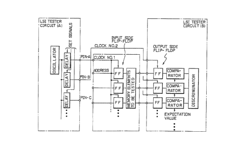
In Fig. 1, the output of an oscillator is fed to
each delay circuit and set signals are delivered to the
delay circuits to generate a clock signal No. 1, and~a
clock signal No~ 2. The clock signal No. 1 is fed to
the input side flip-flop circuits and address signals
are fed to the flip-flop circuits to send the output of
the flip-flop circuits to memory elements to be tested.
On the other hand, the clock signal No. 2 is fed to the
output side fiip-flop circuits. Each output of the
output side flip-flop circuits is fed to each of the
comparators to which the expectation value is applied,
respectively, and the outputs of the comparators are
sent to a discriminator.
In the system of Fig. 1, two clock signals having
different delay times are supplied to the input side
flip-flop circuit and to the output side flip-flop
circuit through the terminal pin PIN-A and through the
terminal pin PIN-B, respectively.
~2f3~ ~ 09
-- 4 --
~ test system for a RAM according to an embodiment
of the present invention will now be descxibed with
reference to Fig. 2.
In Fig. 2, a clock pulse is sent to a clock pulse
width varying portion 2, where a delay control signal is
delivered to vary the width of the clock pulse. The
output o~ the clock pulse width varying portion 2 is
sent to address latches 4 and an output latch 6 simul-
taneously. The address latches 4 sample new address
signals by a leading edge of the clock pulse and the
output latch 6 is latched by a trailing edge of the
clock pulse (Sample is carried out also from the leading
edge timing), thus comparing the output of the RAM 1
with the output expectation value responsive to the
address access time of the RAM 1 by a comparator S or
exclusive OR circuit. The exclusive-OR gate will
provide an output (logic 1) only when the two inputs are
not alike. This means that the two inputs must have a
different logic level in order for a logic 1 output to
occur. Note, for the exclusive-OR gate, an output
(logic 1) results only in steps when two inputs are "O",
"1" or "1", "O" where the inputs have a different logic
state.
The exclusive OR gate is used in binary word
detection. For example, when two input words are
identical, the output is low. If the words are not
identical, the output is high. This type of word
comparison is very helpful when searching through a
large amount of data or words for a particular word.
The number of times the word occurs can be counted with
this circuit, by providing a frequency count of the
word. The address access time of the RAM can be measured
with high precision by the comparator output. Moreover,
the pulse width of the clock pulse can be counted by
measuring the clock frequency by a frequency counter.
By using the detailed circuit diagram of important
parts of Fig. Z, the embodiment of the present invention
74C19
-
will be described in detail with reference to Fig. 3.
Figure 3 is a detailed circuit diagram of a clock
pulse width varying portion 2 in Fig. 2.
The clock pulse width varying portion is composed
of a variable delay circuit by twenty-five stages of
ring oscillators and a chopper circuit which determines
the pulse width in response to the delay time. Based on
such a constitution, the requency of the output clocX
is measured to determine its pulse width with a high
accuracy.
A clock from an LSI tester is input to a terminal
201, and a ring oscillator enable signal is input to a
terminal 203. The clock pulse, which is controlled to a
predetermined pulse width, is output from a terminal 204
and sent to an address latch 4 and an output latch 6
(Fig. 2). A delay time control signal generator 21
generates a delay time control signal and sends it to a
decoder 22, and then after a decoding operation, the
output of the decoder 22 is sent to five NOR circuits
No. 17, 19, 21, 23 and 25.
Each numeral of the NOR circuits D~Y (1) to DLY (25J
represents a relative amount of delay of a clock signal.
Therefore, when the ring oscillator enable signal at a
terminal 203 is LOW and a signal is sent which selects a
path 221 by a decoder 22, the delay time Td25 of the
twenty five stages of ring oscillator can be measured at
a frequency counter (not shown) which is connected to
the output of the OR circuit 23. As a result, when the
data paths 221 to 225 are selected respecti~ely, the
chopped pulse width tWC can be calculated. For
example, in tile case of the data path 221,
twc Td25 x (17/25) = Tpl
The same holds true for the paths 222 to 225,
Tp2 Td25 (19l 5)
P3 d25
Tp4 d25
T 5 = Td25
,
"` ~2~37~ 9
The operating test of a R~M is carried out so that
the standa~d ~alue TAACK for checking an address
access time TAA of a RAM 1 may be previously determined
and the data path having the condition
Tptn~ TAACK ~ Tpn
may be utilized.
Therefore, irrespective of the precision of the
clock pulse width given by an LSI tester, a clock haviny
a pulse width with a good precision can be output by a
clock pulse width varying portion 2 (Fig. 2~.
That is, in response to the pulse width of a clock
pulse output from the clock pulse width varying
portion 2, the address access time TAA of the RAM 1
can be precisely measured.
Figure 4 is a waveform diagram of each portion in
Fig. 2. In Fig. 4, item (1) denotes an address signal
S (3) in Fig. 2, item (2) a RAM output S (1), item t3)
an expectation value S (EXPECT), item (4~ a comparator
output S (5), item (5) a clock, and item (6) a resulting
output S (6), respectively.
First, an address data is applied to an address
latch 4 to produce an address signal. The address
signal is applied to a RAM 1 to output the data. The
waveform of an old address is changed to that of a new
address, and accordingly, the RAM output is changed from
"1" to "0". In the region of a minimum time to a
maximum time, the level of RAM output is not fixed.
Correspondingly~ the output expectation value is also
changed from an old value to a new value. The changing
point of the expectation value is a little earlier than
the changing point of the address signal. In response
to the changing point of the output expectation value,
the output of a comparator circuit varies from a
coincident region to a non-coincident region and returns
to the coincident region.
When a common clock pulse is supplied to the
address latch 4 and the output latch 6, the address
latches 4 sample new address signal by a leading edge of
the clock pulse, and the output latch 6 is devised to
close the latch by a trailing edge of the clack pulse,
thus comparing the RAM output with the output
expectation value responding to the address access time
of the RAMD For example, when the latch output at the
output side is changed rom "1" to "0", i~ the latch is
closed, and if the latch is definite, the "0" output is
produced. As a result, the address access time o~ the
RAM can be measured with a high accuracy.
After the output of the RAM 1 and the output
expectation value are compared and the result of the
comparison is latched by the trailing edge o~ the clock
pulse at the output latch 6. If the clock coincides
with the resultant output of the latch, the output
is "O".
The cells within the RAM 1 are selected by the
address output of the address latches 4 and ~he output
responsive thereto is fetched from the RAM 1. For a
period when the output and the output expe~tation value
are compared by the NOR circuits 51, 52, 53 in Fig. 5.
During that time, the NOR circuits 62, 63 are left open
and the output latch portion 6 is closed by a trailing
end of the clock pulse, and it is determined whether or
not the output of the RAM has reached the value of the
output expectation value. By varying the pulse width of
the clock pulse, the time period from the opening time
to the closing time of the address latch and the output
latch, that is, the time duration responsive to the
pulse width of the clock pulse, enables the address
access time o.f the RAM to be measured.
Figure 5 is a waveform diagram showing the signals
appearing in the princip~l parts in the device of
Fig. 2.
In Fig. 5, item (1~ denotes a cycle period, item ~2)
a clock, item (3) a latch input S (3) in Fig. 2, item (4)
a latch output S (4), item (5) a RAM output S (1),
~L~r37409
item (6) an expectation value S (EXPECT), item (71 a
comparator output S (5), item (8~ a resulting output
S (6~, and item (9) a tester strobing pulse, respec-
tively.
In each cycle period, a clock is generated,
Responding to the latch input S (3) and the latch output
S (4), the RAM output S (1) is generated~ but the level
of RAM output is not fixed from the minimuEI time length
to the maximum time length.
When the expectation value changes from "1" to "0",
the comparator output is generated, and responding to
the open and close state of a clock, the resulting
output S (6) is obtained.
Figure 6 is a detailed connection diagram of a
comparator portion and an output latch portion in Fig. 2
of the present invention.
In an embodiment of Fig. 5, the output of RAM 1 is
of 4 hits, which possess a plurality of complementary
outputs (+Q, -Q). The RAM has generally only eithex
output (as an example, +Q3, and has a complementary
output (in this case, -Q~ within the RAM.
In Fig. 2, the output terminal of clock pulse width
varying portion 2 is connected to an address latches 4
and output latches 6. The output of the address latch 4
is connected to an address input (AD) of the RAM 1. The
outputs of the address accessed RAM 1 are obtained
respectively as each set of complementary outputs ~+Q0
to +Q3 , (-Q0) to (-Q3)), and after a wired OR
operation, are connected to the first input of the NOR
circuits 52 and 53.
The comp~rator portion 5 is composed of eight
emitter follower type transistors 501 - 508 and three
NOR circuits 51, 52 and 53. The eight outputs of the
RAM 1 are divided into true side wired OR outputs
(~Q0 ~ ~Ql ~ ~Q2 ~ and +Q3) and inversion side
wired OR outputs (~Qo ~ Ql ~ Q2 ~ 3
send each first input to the NOR circuits 52 and 53.
,S37 L~ Q 3
The output expectation value is input to a NOR
circuit 51, the non-inverted output is sent to a second
input terminal of the NOR circuit 52, and the inverted
output is sent to a second input terminal of the NOR
circuit 53, respectively. Th~ non-inverted output of
the NOR circuit 61 is connected to each third input of
the NOR circuits 62 and 63, and the inverted output is
connected to the first input of the NOR circuit 62
Each output of the NOR circuits 52, 53 and 62 is
connected to the first, second and third input terminal
of a NOR circuit 63. The output of the NOR circuit 63
is connected to the second input of the NOR circuit 62
and, at the same time, fetched out as a resulting output
of the output latch portion 6.
Figure 7 is a waveform diagram of each portion of
Fig. 5. After four true side wired OR's t~Qo ~ +Ql
+Q2 and +Q3) are connected to the NOR circuit 52,
the first input A is changed from "1" to ~0It and the
second input B is constantly equal to "0". ~he outpuk
of the NOR circuit 52 is shown by a waveform C and the
resultant output is shown by a waveform output. The
non-inverted output of the NOR circuit 61 is shown by
the waveform D and the inverted output by the waveform E.
- The output of the NOR circuit 62 shows the variation
from a LOW level to a ~IGH level and the latch is
closed.