Note: Descriptions are shown in the official language in which they were submitted.
CIRCUIT ARRANGEMENT FOR GENERATING ~IIGH VOLTAGE PULSES .
Technical rield
. ,
The in~ention relates to a circuit arrangement for generating
high voltage pulses from DC voltage comprising a transformer, a
5 secondary winding and at least two primary windings of said trans-
former, said primary wind-ings, at least one diode and a switching
circuit are serial connected; said series circuit is connected to a
voltage source~ a capacitor i9 connected to the common terminal of
said voltage source and of said primary windings7 further said
10 switching circuit is formed from the emitter-collcctor~section of a
switchin~g transistor, on the base of said swi-tching transistor the
outpu~ of a transistor amplifier is connec-ted and ~he input of ~said
transistor amplifier is coupled with the output of a control circuit.
The generating of pulses, especially of high voltage pulses
is frequent~r needcd in the ~lec-tro-technics and electronics~ This
demand occurs very often in the Pield of the ~ehicle electrics, where
the high voltage sparks for the ig;nition ol int~ernal combus-tion motors
are generated b~ high voltage pulses . Such high ~rolta~e pulse3 are
used to the ignition o~' fLash tubes too, which are applied ~ot only in
the phototec~mics9 but also in -traffic control systems and many other
technical fields. We describe the invention in relation with ignition
systems of internal combustion motors, ne~rertheless the inventlon is
not limited to this technical field.
B ack eround ;~rt
~ .
Electronic ignition systems of internal combustion motors are
commonly us~d, which systems may be divided into two groups. In
tlle .rirst sr~ol~p Lllcrc are the so-cullcd thyristor or capacltive ignition
~, .
. ~ .
.~
: .. . . .. . -
., : . . . . .
; ~ .
3,.
_ 2 -
systems; in such a system a capacitor will be charged and the
stored energy of this capacitor will be switched on the primary
winding of the high voltage transformer by means oP a thyristor at
the instant of the ignition. The ad~rantage oF such systems is -that
the contact breaker, which controls the ins-tant of -the ignition,
switches very small current only, therefore the 'lifetime of t~e
contact breaker increases. The drawback of such systems is
however that an inverter is needed -to charge the capacitor, whic'h
owmg to its structure needs -many components, is expensive, and
durina the short time between two pulses only a limited amoun~
of energy can be stored in the capacitor at acceptable cost.
To the second group of electro-nic ignition systems
belong the so-called transistor ignition systems; in such a system
not a contact breaker~ but a switching transistor circuit ls serial
connected to the primary winding of a conventional igni-tion coil.
In such a systern-the contact'breaker is disburdened too, since
it generates a control pulse of very small current only and a
swllching tr~ sisl:or i9 us~d to intarrupt the high curren-t of the
primary wind~ng. The advantages of such a system is the dis'burden~
i-ng of the contact break¢r, and that higheAr curx ent pulse g can
'be interrupted in the primary windlng of the ignition coll.
It i9 well known that the quality oP the combustion in
an internal combustion motor as well as the efficiency oP the motor
can be impro~red in that way that the i~nition of the fuel will be
effected more perfectly, and this is possi~le by increasing the
energy of the igzLition spark.
As we mentioned, irL capacitive ignition systems the
increasin~ of the energy o~ the spark i5 li7ni-ted by the com-plexity
and cos-ts of the system. The energy converting efficiency of
transistor ignition systems is relatlvely low. The energy of the
3~) higll voltage pulse as well as that of the spark changes significantly
. , ~ , ' ~.'. ' ' :
-, .. .
,
.
3~78
3 --
wiLh thc c'h..lnge of Ihe supply vol:tage, alld this h~mpc~rs especL.l.'1.ly
the cold sLarting o.f intern~-Ll com'bustion motors of vehicles. f~'3
i-t is w-ell known9 at cold star-t.ing the s-tarting electric -motor reduces
tlle voltage of -the cold starter l~attery to such an extent -that thi.s
reduced ba-ttery ~roltage is Prequently not enough to generate the
igni-tion sparkO
lt is the ai-m of the 'Il-~mgarian patent appl.lcation
"Circuit arrangemen-t for generating high vol-tage pulses'l w-Ltn the
laying open nullLber T/31.483 -to eliminate -these drawbacks~ in
which the primary ~inding of the hi~gh voltage transfo~rrler is divided.
in-to two windiTIg parts. In this known circuit one of -the pr-ilnary
wirldings of the treinsformer as wel.l as a switching ciL~Cuit ~ind a
capacitor form together a loop circuit. Both pri.mary windings are
serial connec-ted and over a diode -they are connected Lo a vol-tage
1.5 source. The operation principle oP this circuit is. tha-t at the in.stant
of switching on the switching transi~stor Porming a switching circuit
the stored energy oP the capacitor drives currcnt t'hrough one v~
the primary windings of the transformer, which current adds i-tself
to the current f~owing from the voltage source and by this way a
sigmificcmtly higher current pulse can be generated throu~l the
primary ~inding .
lt is th.e advc-Lntage oP this circuit l-hat at the :interruptin~
of the current .flowing througl~l the primary wirLding~ -that is w'hen
the switching-transistor switches off,, the voltage arising in the
~: 25 ot'her prilrnary winding with opposite polarl~y and chEI.rges the capacitor.
In this way this is can energy recovery circu-it9 since the in.d-uced
v~ltage arising at t'he interr-uption of the current ch.arges ov~r the
energy s-tored in th.e transform.er into -the capacitor. In -this wa~y
this is an energy recovery cîrc,uit. Although this circuit wor-ked
well in the practice~ -the-~inding used to ener~y recovery does not
work at generating tltLe spark.
~ .
'' ,'
,
. :' ',' ~: ' '
~ 4 ~
In the circw.-t arralLgernents descri.bed above theore-tiea'Lly
electromec1lanical switching devlces could also 'bc u.sed as sw:i-t:ching
circuits, yet these haYe so many drawbc1.cks tha-t in electronic i~rlit:ion
s~stems the~r are -used at most l1S control swit.:~.es. 'I'o interrup-t
'. 5 the high current fLo~ing through thc~ primary win('Lul.g o.P the truns-
îormer high power witchin.g-transistors come a:t~ove all into considct.~lt~
ion. I 'have used such a transistor in the i~gnition sys-tem a ccordlng to
my above mentioned pa-tent applïcation ~-I'iJ_PS T /31.483. In Lhis
'k:lown circuit the switchîng transistor is actuated by a transis-to-r
amplifier, which is controlled 'by a con-trol circuit. A negative :l~eed- -
back circuit i5 applied comprising a voltage dependent resistor so
that lest -the changing, Pirst of all the reduction o:f t~le supply vo'ltage
may si~nificantly reduce the energy oP the pulse. This vol-tage depen-
dent resistor - taking into consideration the Low supply voltage7 the
1~ needed characteristic and -the va'Lue of the resis-tor ~ should be an.
incandescent lalnp~ yet the dimensionsg liPet-~me an.d relicLb-i'lity oP
which are disadvantageous compared to other components, a:Qd this
is wl~y the practiccll a-pplicabi1.ity o.P this circuit arrangemen-t is limited.
l'he in~ren-tion hns Por its objecl: to provide a circ-ui-t
arran~emerLL descri'bed in the openLn~ paragrapll~ which should conibine
tlle ad~clllt..~ges oPb~th the capacitive and the transLstor ignition systrrrs;moreo~er the stored magnetic energy should be rec:overable wlth t;1le
best possible e:FPiciency and by this way the efPiclenc~r of th.e gene:rat~
ing the high voltage pulse should 'be improved. Another airn o~-the
inven-tion was to form such a switching circuit, by means of which
the elle~rg~y Or the high voltage i.mpulse could be kep-t cons-tan-t ~uldex
a supply v~l-tage changing withi-n broad limits, what wou'ld be very
advarLtageous especially to cold s-tarting of in-ternal com'bustion motors
of vehiclesO
..... , . ~
. . . .
. .
.
.
. ~ ' ' ~ .'", -
~: .
- 5 - 27573-g
Disclosure of the Invention
_
I achieved this object by means o~ the circuit arrange-
ment of the kind mentioned in the opening paragraph in that the
input oE a transistor amplifier is the base of a second transis-
tor~ between said input and the output o a control circuit two
serial connected resistors are inserted, to the common terminal of
both said resistors the emitter-collector-section of a first
~ransistor is connected, to the base of the first transistor a
voltage di~ider is connected, the branch of which standing on the
collector side is divided and connected to a voltage sour~e
between the dividing point of said branch and the common terminal
of a primary winding o~ a transformer and of a switching
transistor a capaci-tor is inserted, a resistor of said voltage
divider inserted on the emitter side is connected to a current
control resistor whi.ch i5 in series with the
emitter-collector-circuit of said switching transistor.
In accordance with a broad aspect of the invention there
is provided circuit arrangement for generating high voltage pulses
from DC voltage comprising:
a transformer including a secondary winding and at least a
first primary winding and a second primary winding;
a rectifying means connected between said first primary
winding and said second primary winding;
a first capacitor connected in parallel with said first
primary winding and said rectifying means and in series
with said second primary winding;
switching means, comprising the emitter-collector-section of
~,~
.
-
~'
7~
- 5a- 27573-9
a switching transistor connected in ~eries with a
current sensing means, connected in series with said
rectifying means and said first and second prim~r~
windings to form a first series circuit;
means for connecting said first series circuit to a voltage
source;
: a control means;
an amplifying means;
first connecting means for connecting an output of said
; 10 control means to an input of said amplifying means;
. second connecting means for connecting an outpu~ of said
~` amplifying means to the base of said switching
:~ transistor;
said first connecting means further comprising first and
second resistors connected in series, the common terminal of said
: first and second resistors being connected through the emitter
: collector-section of a first transistor to a first
. .
: terminal of sai.d voltage source connecting means, and
,:
a voltage divider connected to the base of said first
transistor, wherein said voltage divider comprises a
first leg including a third resistor and a second leg
~: including a fourth resistor and a fifth resistor
: connected in series, said first leg connected to a
terminal between said switching transistor and said
~- circuit sensing means, said second leg connected to a
~ second terminal of said voltage connecting means, and a
' :
, . , , . . -
- . , ~
., . ,. :
: . . : . :
~3t~
- 5b- 27573-9
terminal between said fourth and fifth resistors
connected through a second capacitor to a terminal
between said switchlng transistor and said primary
windings.
; In accordance with another broad aspect of the invention
there is provided circuit arrangements for generating high voltage
pulses from DC voltage comprising:
a transformer including a secondary winding and at least a
first primary winding and a second primary winding;
a rectiEying means connected in series between said first
primary winding and said second primary winding;
a first capacitor connected in parallel with said first
primary winding and said rectifying means and in series
tO with said second primary winding;
a second capacitor connected in parallel with said second
primary winding and said rectifying means and in series
with said first prirnary winding; and
switching means connected in series with said rectifying
means and said first and second primary windings to form
a series circuit;
means for connecting said series circuit to a voltage
source.
The advantage of this circuit arrangement is that by
means of the applied double feedback very steep switching of the
~: switching transistor can be achieved and in the same time the
energy of the generated pulse keeps practically constant even by
reduction of the voltage of the voltage source by over 50%.
-~ In the circuit arrangeme~t according to the invention in
''~ .
. ,: . , . ,. . . ,, : :
- 5c- 27573~g
a control circuit a series circuit comprising a pair of actuating
contacts, a resistor and an induction coil is connected to said
voltage source, the base-emitter-section of a transistor is con-
nected parallel to said induction coil having such a polarity that
the voltage arising in said induction coil at the interruption of
the current switches on said transistor, and the output of said
control circuit is formed by the collector of said transistor.
The advantage of this circuit arragement is that the structure of
it is much more simple than that of the above mentioned
HU-PST/31.483; in the same time the voltage pulse generated by the
interruption of the current of the induction coil gives rise
'
.
.
' : ,
7f~
~ 6 ~ 27573~9
to a fas-t and definite switchin~.
It is further advantageous that between the base of said
transistor and ~aid induc-tion coil a voltage divider is inserted.
Expediently between the collector o~ said transistor forming the
output of saicl con-trol circuit and said current control resistor a
capacitor is inserted~
An advantageous embodiment of the invention aims to
accelerate the switching, in which a capacitor is connected paral-
lel to said resistor, which is serial connected to the input of
said transistor amplifier.
A Eurther circuit arrangement according to the inventionis also advantageous to achieve the set aim, which comprises a
transformer, a secondary winding and at least two primary windings
: of said transformer, said primary windings as well as at least one
diode and a switching circuit are serial connected, said series
circuit is connected to a voltage source, a capacitor is connected
to the common terminal of said voltage source and of said primary
windings, and which according to the invention is characterized in
that said diode is inserted between both said primary windings,
said capacitor is parallel connected to said first primary winding
attaching itself directly to said voltage source as well as to
said diode connected serial to said first primary winding, and a
further capaci-tor is parallel connected to said second primary
winding, as well as to said diode is connected serial to said
second primary winding, and said diode is inserted in forward
direction in respect o~ the polarity of the voltage
:
.,.~ .
J .~
', ~ .
- ': : .
.:,
,
~ ~3~37~
_ 7 _ 27573-9
source. This last circuit arrangement has the advantage that at
generating the pulse a significant part o~ the energy supplied
into the trans~ormer can be recovered by the way that the magnetic
energy stored in the iron core at the instant oE the interruptiny
of the curren-t is charged over into the capacitor and stored in
it, and afterwards this stored energy will be utilized to the
energy of the following pulse.
Brief Descri~tion of the drawings
Fig. 1 is a circuit diagram of an energy recovery cir-
cuit of the transformer according to the invention,
Fig. 2 is the equivalent circuit diagram o~ the circuit
diagram o~ Fig. 1 at the instant of the switching on;-
Fig. 3 is an embodiment of the switching circuit accord-
ing to the invention;
Fig. 4 is the waveform o~ the current flowing through
the switching circuit according to the invention; and
E'ig. 5 shows the application of the switching circuit
according to ~he invention in the energy xecovery circuit o~ the
above mentioned Hungarian patent HU-PS T/31.483.
Best Mode of ~arrying out the Invention
In Fig. 1 the primary windings 2 and 3 o~ the trans-
~ormer 1 o~ the circuit according to the invention can be seen
only, between which a diode 8 i5 inserted. The diode 8 is insert-
ed ln forward direction in respect o~ the polarity o~ the voltage
source 7. Capacitors 12 and 10 are through the diode 8 parallel
connected to the primary windings 2 and 3 respectively. The
,~.,,.,~
- . . .
.
~ . ' .
.
~ ~3'7~7~3
- 7a - 27573-9
terminals of the capacitor 12 are connected to the positive pole
oE the voltage source 7 and to the cathode oE the diode 8
respeckively. The terminals of the capaci-tor 10 are connected to
the anode of the diode 8 and to the terminal of the primary
winding 3 standing toward -the negative pole of the voltage source
7 respectively. The switching circuit 6 is inserted between the
primary winding 3 and the negative pole o-f the voltage source 7.
The function of the circuit shown in E'ig. l is as
follows.
At switching on the switching circuit 6 current begins
to flow from the posi-tive pole through the primary winding 2, the
; diode 8,
; ~
,,~ i
,
'- . .: ' ,, : ' .
-
,
~3-
t}~e pr~ r~ ;y ~ind:ing 3 and the swil:cllin.g circui-t 6 into the negative po'le
. ol! thc ~roltage source 7. Meanwllile magnetic energy is accurnulated
in the prima-r~ wind-i-lgs 2 and 3. ~t switching ofP the switching circuit 6
the c-LIrrent is -inLerrupted through the primar~ windings 2 and 3 and
5 a voltage j~unp of opposite polarit~ to the former voltage arises on the
tcrmill~lls of ~le primr-rsr-w-indings 2 and 3. ~ccordingly-the terminal of
thc primar;y wuLdillo 2 connected to the diode 8 will be o:f posi-tive -polarit~and -the -tcrnlirlrLl of the primar~r windin.g 3 connected -to the cathode oP
tl~c diock! S wi'Ll be of neg.ltive po'larity. ~t this instant the primrlry
() WillClillg9 2 ancl 3 can l)e corLsidered as voltage sources ~-Lnd with -the
sakl pola.ril::ies the dio.:le o is in conducting sta-te. T'hus :~le stored
m.<lollctic encr~ of t.hc primary winding 2 flows -through the dio-le 8
UlLO the caE~aLcitor 12 and will be converted in-to electrostatic ener~y
- sLored in the capacitor 12. Similarl~r the voltage jump arising in -the
1:5 plinla.ry winding 3 c~.arges the capacitor 10 through the diode 8~ `~fhen
the magnetic energ~r o.f' the primary windings 2 and 3 has l~een fully
overcllrlrged into the capa.citors 12 and 10 respectively~ the voltage on
the terminals of` the primar~r wind-ings 2 and 3 ceases and the diode 8
switches off. 'L'he circ~it res-ts -in this corndition.
~t tlle in~s~ nt o.f swi-tchirLg on aga-Ln -the voltages of the
cnprlcitors 12 ~md 10 will rldd theln~selves to the volta~ge of' the voltage
.source 7 ancl ~ since tlle diode o :is s-till in off s-tate - the capacitor l.2wi'l.l 'bc disch.rl.l ged Lhrou.g]l t'he primary windi:ng 3 and t'he capacitor 10
through the primary win(ling 2 respectively. Taking into consideration
2::) thrlt tll.e capacitors :1.2 ~.rnd 10 caIl be charged up to a hig'her voltage 7 a
higl~ current pulse arises through the primary winding~ 2 and 3. When
the charge of the capacitors has been used up, that is their voltages
ha~re decreased, the diode ~3 renders conducting and a current oP the
same direction .~lows t.l~rough t:he primar~r windings 2 ~d 3 and the
o~) diode S bet~ve~n -them ~f'rom th~ vo'].itrlge source 7. Under the influence of
~hc l-igh CUI rent pulse l'Lowing throrgll the primary windings 2 emd 3 ;L
,
.
- . ,,
. : . : .. .. . ,: .,
': ' . , , . ~ : ' , '-
'7~7~,
hi.gll vollagc pulse arises in the secondary w-ind-lng of the high voltage
trans:~rmer not shown here. or course -the voltage source has to ~e
sui-tal~le -to lead through -the high current pulse a-t the instant of thc
dischargc of -the capacitors 10 and 12. This is easil~ possi~ble in the
case of having a starter battery.
~ft~r -the capacitors 12 and 10 have transmitted their energy
to the primary windi~gs 3 and 2 respectively in form of said current
p~iLses~ th~y lose their charg~s, their voltages cease and afterwards
tlle currcnt ~lowing ~rom the voltage source 7 -through -the primary
1~) windings 2 .~nd 3 accumulates magnetic energy again in the iron core
of -the high voltage transformer ~:. Thereafter under the in:Quence
Or the repea-ted switching ofP and on of the switching circuit 6 the
process mentioned above occures repeatedly and accordingly high
voltage pulses arise.
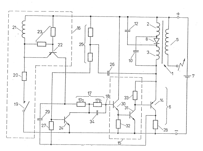
In Fig. 3 the practically realized switching circuit according
to the invention is shown wi-th t'he above mentioned circui-t arrangement
a'lso accord-ing to t'he invention. In this circuit arrangement the trans-
former 1 comprises two primary windings 2 and 3, between them a
~, diode 8 is inserted with a polari-ty that ln respect of the poklri-ty
Or the voltage source 7 the diod~ 8 is in Porward direction. 'rO ~he
common tcrmin.Lls l)c-tween the cliode 8 ~mcl l:hc prim~lry windin~ 2 or
rather the primary winding 3 capacitors are conncct~d in su'cil a
wny that c~Lpacitor 1() is connec-ted to the ~mode of the diode 8, the
oLIIcr terlll-inal Or wllicl~. Ls conn~cted to tlle t~rmirla'L of the primary
win(ling 3 st~Lding toward the negative pole of the vol-tage so~rce 7.
J rO -the cathode of the diode 8 capacitor 12 is connec-ted, the other
terminal oP which attaches itself to the terminal of the primary winding 2
standing toward the positive pole of the voltage source 7. The trans-
former 1 comprises a secondary w-inding 5 in which ~mder the irlfluence
of thc current pulsc describcd in connection with Fig~ 1 and Fig. 2
r~ s pc c-tively hig~) vo I-tagc pulsc ~Irise s,
.
.~: , , -, . ., - , ~ .
.
,
- ' '' ' ' ',: , . - .
~ "
~37~
- 10 -
In tlle switching circuit accordLng -to t'he invention shown
in E~ig. 3 the switch ing circuit 6 is formed by a switching tran-
sistor 14. The switching transistor 14 is con-trolled by a con-tro'L
circuit 16 over an inserted transistor amplifier 15. ln the -transis-tor
amplirier 15 transistors 30 c~Ld 31 f'orm together a two stage d. c.
amplirier. ~ the e~ample shown he-re the transis-t:or 30 is an npn
l:ransistor in cormnon collector circuit and a resistor 32 i5 irLSerted
in its emit-ter circuit. To the emitter of the tr~msistor 30 the base
of a transis-tor 31 is connectecl, which is in common emit-ter circuitO
The transistQr 31 has a load resis-tance 33 in its collector circuit,
thc other ter-m-inal of which is connected -to the ~mitter oP the
switching transistor 14; which is in this example in common collec-tor
circuit and is formed by a pnp transistor. The input 18 of the
- transistor c~lplifier 15 is the base of the transistor 30. A resistor
17 is seriaL connected to the input 'l8, which -in an adv~n-tageous
embodiment is divi~ed into two parts~ w'hich are formed Prom the
resistors 17a and 17b.
'Ihe output of a control circuit 16 is connected to -the ~nput
18 of the lransistor amplifier 15 over the resistors :L7a and 17b.
In the control circui-t lG a pair of actuatirlg contac-ts 'l9, a resistor
20 ~nd all induction coLl 21 are connected in series to the volLage
source 7. ~n applic:a-tions -to intel~nal combustion motors the pair
of ac-tu~tirLg contacts 1~ is formed by the contact 'breaker oP the
nlotor The 'base~.emitter-circuit of a transis-tor 22 is paralle'l
connected to the induction coil 21. It may be practical to inser-t a
voltage divider 23 into ~Le base circuit, which divides the vol-tage
going to the base.
The funcLion of the switchlng circ~rit 16 is - partl~ on the
'basis of -the waveform shown iD Fig. ~ - as follows.
At closing -the pair of actuating contacts 19 a currerlt be~s
.
;'
.
. . ' ~
- ' , ::,
3 ;r~
Lo fLo~ -throu~h the resistor 20 and the induction coil 21, and. therl
~lle curren-t flowing through the induction coil 21 will be -interrupted
arLd a vol-tag~ will 'be induced in i-t, -the polarity of which is such
th.lt a. posi-tive volta~e jump will ge-t -to the emitter of the transistor
22 and a negative voltage j-unp to the base oP tlLe same It is -to 'be
noted -that in th.e exal-n.ple s}lown here the tran.sis-tor 22 is of pnp
type. 'Under l:he i-nflllence of the voltage jump o.f the induction coi'L 21
the transistor 22 switches on and. .frorrL the vo'Ltag~ source 7 through.
~ e induction coil 2'1 .-n.d the em-it-ter-collector-circuit of the transistor
IU 22 a forward voltage gets to the input 18 o~ the transistor amplifierl5. 'rO the outp-ut of I'he -transistor amplifier 15 a capacitor 29 is
connected - this we shall mention later again -, which is important
in respect of the forming of the waveform on the i.nput 18. When urLder
the influence of the v~ltage pulse appearing on the induction coil 21
the transis-tor 22 switches on7 -then the current f~owing throu~h its
emitter-collector~cLrcuit is driven not only'by the voltage o:t` tlhe
voltage source 7, bu!: also by the vol.tage pulse connected serial to
the former arising in the induction coil 21.
To t'he dividillg point of the above men-tion~d. divided r esistor
'L7 I~-tw~en the resis-tors ].7a ancl 17b - which i9 principall;y the divlde~l
Input poi-nt or the input 1.8 - the emitter-collec-tor_circui-t of a first
~:ra.n~sistor 2G is para.llel connec-ted. 'E3y this wa~r t'he input 18 of th~
Lransistor ampli.Pier 'l.~ as well as the switch-ing tr~sis-tor 14 is in
off colldition~ when the first transistor 24 is in. conduc-t-i:ng condition.
Between the collectol of the switching transistor 14 and the nega-ti~re
pole of -the vol-tage source 7 - the latter is generally an earthed pole -
a current control resistor 28 of ver~ low value is inserted. The
value of this current control resistor 28 is a few mOhms only, there-
fore practically it does not limit the current flowing through the
:~ 30 s-w-itching transis-tor lG as well as the primary windings 2 and 3 ofthe -transformer 1. To -the base of -the above mentioned first transistoL 'i '
a voltage d-i.vi(ler is conrlected, th.e resistor 27 of which ka~ing on
the emitteL si:le com~ cted to th~ current control resistor 28~ e
:
'
.~
. ' ,
.
:. , , . , - . : . .
- . ~ -
' ,~
-
c~78
- 12 ~
isto1 ~5 of t:he sr~ e volLage di.vi.der beirlg on the collector sicLe i;
e~r~ cL(~d Lo 1t1e ~>osi.ti.ve pole Or tl1e vo].t~ e source 7 an(1 is (:Livicled-n~ t~ - in. 1:wo resi.stors. 13etween l:hc diVidirLg poilll: of li~C'Se t~o
r ~ .ol-s an~ e conlnlon terrr~ l of t1-lr.? swi-tching-tran.sistor 14 ~Ind
o1 L11e tr.1n rO1 rn.er I a crlprlcitor 26 is inser!:-d. 1:his capr1ci-tor 26 prod-uces
a ~o1.tLIge fec ~lt)ack to t.tle base of Llle first transis-tor 24 ancl in -thr same
~ime thc vol.tage arisil~ on -the cu.rrent colltLol resistor 2c, - which
vol.tr~ge Is proportiona. -to the current ~ produces a current feedbrtck
to the base of the same first transls-tor 2G.
lS.) The fw~ction of the circuit arran.gemen-t oi` Fig. 3 can
be followed up on basis of Fig. 4 too
E;ig. 4 Lshows the -waveform of the curren-t I :~Lowing
through the primary wind:ings 2 alld 3 of th.e -transPormer I~ the switcning
tr~lnsistor 1.4 ancl the c ur-rent con-trol resistor 2$ as the l`unctiorl of
1. ~ ti111C t. ~t point .~ the switching trr.-nsistor 14 swi1che~i on and~ as -it
hr1s ~cendcscribec1, thc? ca-pacitors 10ancd :12 connecl:e(l serirll to the
voltr1~e source 7 givc r ise to rl.hi~;h currcnt pulse~ which increascs
up l:o the pOi11t 13. At r~aint 13 thr cllarge o.l! the ca:paci-tc~rs 1.0 arlcl 12
: ~ hrl.s 1)~en usecl UE~ an~ ~he~ currrent L decLa~ls~!s up to ttlC point C. rhi3
~C) current pul~e incluces ~1 high volta.ge puLse in the secondary w1.ndLLlg o.1
the tralls~ormer 1.
On t.he c:urrent control resistor 28 a vo1tage arises, wtlich
i.s proportional to the. cu.rrent I. I~his voltage adds itself -to the vol-tage
stored in the capacitor 29 and this results in that: the transistor 30
2j as well as the switctling tr~msistor 14 rests in on s-tate further on, wh
-the Lransistor 22 has bee-n switched o~O
This voltage arisin~ on -the current con-trvL resis-tor 28
controLs th.e b~1se of -the first transistor 24 too and -in the vicinity ot`
pOi1l1 13 it ~ kes nn e1i'o:rt to swit~h ~n l:Q rirst transis~or 24. Neverthe- :
>o Le-~ t1)e 1n-lch 11igher l-Le~itive pulse a~ising on ~t1e c~pclcitor 2~ ii? ih
ne time co1:u~.te-r~cts it ~(nd keeps rhe tra:nsistor 2G i-n the ViC:ii1iT: v of
, .,
,
. . . .
': ~ '.......... ':
- 13 - 27573-9
point B still safely in o~f state, therefore the switching off of
the switching transistor 14 safely does not take place. With the
knowledge of the voltage divider of the transis-tor 24, of the
capacitor 26, of the voltage of the voltage source 7 and of the
voltage drop arising on the current control resistor 28 this func-
tion can easily be calculated.
In Fig. 4 after point B the discharge current of -the
capacitors 10 and 12 decreases and at point C the current of the
voltage source 7 only flows through the primary windings 2 and 3
; 10 and the diode 8, which meanwhile has been rendered conductingO
From point C on the current I begins to increase with a slope
defined by the inductivity of the transEormer 1. Reaching point D
the voltage arising on the current control resistor 28 switches on
the additional transistor 24 over the resistor 27. It is to be
noted that the pulse of switching off polarity on the capacitor 26
is now no more present. At the instant of the switching on of the
transistor 24 the switching transistor 14 switches off abruptly
and -the interrupted current I induces a vol-tage of opposite polar-
ity in the primary windings 2 and 3, which charges up the capaci-
tors 10 and 12 agai.n.
The temperature dependence of the transistor 24 is such
that the temperature dependent change of the forward voltage
changes the position of the point D on the diagram I. At lower
temperature the point D moves into the direction of the dash line
- in Fig. 4, i.e. the current I can increase to a higher value.
; This again gives rise to the increase of the magnetic energ~
,~,, .
., .
,
7~3
- 13a - 27573-9
stored in the transformer 1, i.e. -the high voltaye pulse is
practically oE constant energy between broad limits in cold, at
lower supply voltage too. I'his is highly advan-tageous at the cold
starting of vehicles.
It may be advantageous to connect a capacitor 34
parallel to the resistor 17b, which speeds up the switching on the
second transistor 30.
,. ~,,
,
,' ,' ' ' " :
: , - ' ' ' ~ .
~ 3t7~78
- 14 -
L he swi tching circuit ~Iccord-ing to the invention and
~;IIO~Vll in l;ig. 3 is a pplicable to other pulse generating circ-ult too,
Ihe Lr;~lisrorrner 1 of which is completed with an energy recovery
circuit. An example of such a circuit arrangement is shown in Fig. 5.
The primary windings 2 and 3 oi? the transformer 1 as well
as the diode 8 are inserted serial in-to the emitter-collector-circuit
Or the switcl1ing transistor 14. Up to -this point the switching arrange-
ment corresponds to that shown in Fig. 3. The difference is that
the primary winding 39 the switching transistor 14 and a capacitor 34
togetl~c!r ror~n a lopp circuit, as i-t is clescribed in details in the above
menLioned-p~-lent specification l-IIJ-PS T/31.483. The f~mc-tion of the
switclling circui~ according to the invention is the same in this case
too ZlS described nbove.
The al)ov~ described circuit arrangement according-to
-the invc!ntion has been accomodated in -the casing of a conv~ntional
ig-nition transformer. As the control circu-it 16, the transistor amplifier
15 and in some cases the switching transistor 14 are suitable to be
inLegrated together or developed as a hybrid circuLt, so they can be
ezlsily accolrlodzl-ted in the casing of a conventional ignition transformer
together with the high voltage transformer 1. By this way the complete
circuit arrangement according to the invention can be directly exchanged
for Zl conventional i~nition coil used in vehicles today, no additional
device~ equipment or casing is needed. This improves significantly
llle appliczlbility of the circuit arrangement according to the invention.
'
-- .
.: ~ . . . . , :
:, . ~ , . : .
..
;
.. . .