Note: Descriptions are shown in the official language in which they were submitted.
~2~
The present invention relates yenerally to digital
data detectors, and more particularly, to digital data
detectors for detecting digital data from a digital
modulation signal in a digital data transmission system. ~ -
Descrlption of the Prior Art
Conventionally, various apparatuses for detecting
digital data from a digital modulation signal have been
proposed. As one example, a digital data detecting
apparatus is disclosed in Japanese Patent La~i d-Opèn
Patent ~o. 92410/1984. This apparatus detects digital
: data from a digital modulation signal in the following
manner. The dlgital modulation signal is sampled at a
frequency of m ~imes (m ~ 1) the channel bit rate. It is
assumed that the digital modulation signal is sampled at a
frequency of ~wo times.t~he channel bi ~ rate . Sa~p l i ng da ta
Si~l at the current sampling point and sampling data Si at
a sampling point which is located one point before the
current sampling point are used to find a phase interval P
between a point at which the digital modulation signal
. crosses a reference level and the current sampling point
from the following equation. In this case phases of
.
A
~ . ~ . - , . . . .. . . .
. ~. . ... ~ -, ..
. .
.
~ 2~
sampling points are represented by values of O to N-l
obtained by dividing a channel bit period into N equal
divisions;
p = ¦Si+l¦ N/2 ... ~1)
lSi+ll + l5il
where N/2 is a value af one-hal~ of a channel bit
interval. A predetermined value (N/2) is added to a phase
Pi of the sampling point which is located one point before
the current sampling point, to obtain an estimated value
of a phase of the current sampling point. In addition,
the estimated value o the phase of the current sampling
point is corrected by the following equation, so thatthe
phase Pi+l o-E the current sampling point is calculated;
P = {P ~ (Pi ~ N/21}-K ~ P~ (2)
where K is a coefficient of.O ~ K < 1.
on the other hand, ~hen the digital modulation signal
does not cross the reference level between the current
sampling point and the sampling point which is located ane
point before the current sampling point, the phase Pi+l of
the current sampling point is calculated from the
following equation:
Pi+l Pi ~ N/2
A clock in synchronization with the digital
: modulation signal and digital data corresponding to the
clock are detected in response to sampling data at each
- 2 -
- , . .
- .
.
~ ~8~8~
sampling point thus obtained and a phase of the samplin~
point.
Meanwhile, the data detecting apparatus can cope
.. with multichannel input by sampling channels with different
timing and sequentially converting the channels into signals
to be inputted.
: According to the above described conventional data
detecking apparatus, when the digital modulation signal does
not cross the reference level, the phase of the current
sampling point is evaluated by equation (3), so that phase
interval between two adjacent sampling points always are a
constant value N/2. Thus, if fluctuations in the frequency
caused by a wow fl.utter or the like, increase, a phase to be
calculated cannot follow the fluctuations in the frequency,
whereby data is erroneously detected.
Meanwhile, Japanese Laid-Open Patent NoO 222072/1986
q filed by the assignee of the present application discloses a
digital magnetic recording and reproducing apparatus in the
clock extraction is determined hy comparing phase information
before and after sampling data of a reproduced signal with
each othér and comparing magnitudes of the phase differences
calculated from the sampling data with each other and the
- 3 -
. ~
.
~ ~8~7~382
phase information is changed depending on the result of
the determination.
SUMM~RY OF THE INVENTION
An o~ject of the present invention is to provide a
digital data detector in which the erroneous detection o~ data
is slight even if fluctuations in the frequency increase.
The digital data detector according to the present
invention comprises sampli ng data detecting means, phase
interval calculating means, phase calculating means, clock
detecting means and data detecting means.
The sc~pling data detecting means samples a digital
modulation signal at a constant frequency. The phase
interval calculating means is responsive to sampled data
detected by the sampling data detecting means .a n d
~- 15 calculat~s a phase interval ~etween a point at which a
digital modulation signal crosses a re~erence level and
the current sampling point. The phase calculating means
is responsive to a phase of a sampling point which is
located one point be~ore and a phase of a sampling point
which is located at least two points before -the current
sampling point for calculating a phase of the current
sampling point.
Additionally, the clock detecting means is responsive
to the phase o~ each sampling point calculated by the
phase calculating means for detecting a clock signal in
'~
-- 4
~'
" ~,
f,
.
- ,
8~
synchronization with the digital modulation signal. The
data detecting means is responsive to the phase interval, tne
phase of the current sampling point and the clock si~nal
for detecting digital data fro"l tile digltal modulation
siqnal.
In the digital data detec-tor according to the present
invention, the phase of the current sampling point is
calculated in response to the phase of the sampling point
which is located one point be~ore and the phase of ~he
sampling point which is located at least two points before
the current sampling point. Thus, if the frequency of the
the digital modulation signal ~luctuates greatly, the
phase of the current sampling point is precisely
calculated ollowing ~he fluctuations in the frequency~
Therefore, the cloc~ signal in synchronization with the
digital modulation signal is precisely detected.
Consequently, the digital data is precisely detected from
~ the digital modulation signal.
: 20 According to the present invention, the phase of the
current sampling point is calculated in response to the
phase of the sampliny paint which is located one point
before and the phase of the sampling point whioh is
located at least two points ~eore the phase of the
current sampling point. Thus, even if the frequency of
-- 5 --
....~ .~
,
. .
! ' ,- j
.
" ~`.. ' ' ' ' , ' ' ;" ', " '' ' ' ' ' ' ' ' . ', ',
',. ' '' '' ' ' , , ' , . : '
. .
8~
. .
the digital modulation signal fluctuates greatl~ due to a
wow flutter or the like, the digital data detector can
cope with the fluctuations in the frequency, whereby, the
erroneous ~etecti~l of cidta is slight.
These o~jects and other objects, features, aspects
and advantages of the present invention will become more
apparent ~rom the following detailed description of the
present invention when taken in conjunction with the
accompanying drawings.
BRIEF DESCRIPTION OF THE DRAWINGS
Fig. 1 is a block diagram showing a main portion of a
digital data detectQr according to an embodiment of the
present invention;
Fig. 2 is a timing chart showlng a signal of each
: 15 portion according to the present embodiment;
Figs. 3(a) to 3(g) are diagra~s for explaining clock
extraction determining conditions according to the present
e~odiment;
Fig. 4 is a block diagram showing specific structure
of clock and data detec~ing circuits; and
Fi~s. 5A and 5~ are diagrams for comparing a phase of
a s~mpling paint calculated according to the present
embodiment with a phase of a sampling point calculated
according to the conventional example, where Fig. 5A shows
a case in which fluctuations in the frequency of a digital
-- 6 --
r I
,
~ ~ ' ", , , ' ~' . ' ' '
~ ~r~ 8~
modulation signal are small and Fig. 5B shows a case in
which fluctuations in the frequency o~ the digi-tal
modulation signal are large.
DESCRIPTION OF THE PREFERRED EMBODIMENTS
Referring now to the drawings, an embodiment of the
present invention will be described.
As an example, description is made on a case in which
digital da-ta is detected from a di~ital modulation signal
according to an NRZI type modulation scheme in the case of
the minimum magnetization inversion interval (Tmin) =
0.8 T and the maximum magnetization inversion interval
(Tmax) = 3.2 T.
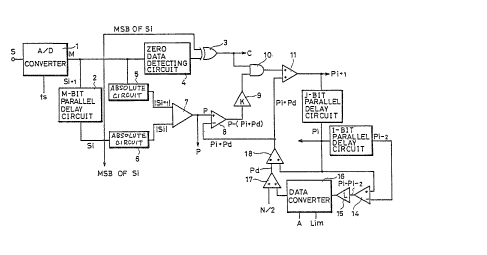
Fig. 1 is a block diagram showing a main portion of a
digital data detector according to the present invention.
In this portion, a digital modulation signal is sampled in
a predetermined cycle, so that sanlpling data at the
sampling point is detected and the position, i.e., a phase
of the sampling point is calculated. In addition, Fig. 2
is a timing chart for explaining an operation of the
digital datà detector.
In Fiy. 1, a digital modulation signal S is inputted
to an A/D converter 1. The A/D converter 1 samples the
~`- digital modulation signal S in synchronization with a
clock signal fs~ to convert the same in-to M-bit digital
data. The frequency of the clock signal fs is m times a
;~ - 7 -
'' ' ~'' ' ' ''
.
,
J ~37~
channel bit ra-te. It is assumed tha-t the frequency of the
clock signal fs is two times the channel bit rate.
Furthermore, in this conversion, the polarities of plus
(+) and minus 1-) of the digital modulation signal are
represented by an MSB (Most Significant Bit) or "O" and
"1" using two's complement, for example.
An output of the A/D converter 1 is inputted to a
M-bit parallel delay circuit 2, a zero data detecting
circuit 4 and an absolute value-circuit 5 as sampling data
(referred to as the current data below) ~ Si+l at the
current sampling point. An output of the M-bit parallel
delay circuit 2 is inputted to an absolute value circuit 6
as sampli~g data (referred to as the preceding data
~below) ~ Si at a sampling point which is located one
point before the current sampling po.int.
The æero data detectlng circuit 4 outputs "1" when
the current data Sl~l is "O" and the preceding data has
negative polarity, i.e., the MSB i5 ~ ' , which otherwlse
would output the MSB of the current data Si~l. An output
of the zero data detecting circuit 4 is applied to one
input terminal 5f an exclusive OR gate (referred to as an
Ex-OR gate below) 3. The MSB of the preceding data
Si outputted from the M-bit parallel delay circuit 2 is
applied to the other input terminal of the Ex-OR gate 3.
The Ex-OR gate 3 outputs "1" when input sig~als applled to
- 8 -
:,
.
.
,
,, :, ,,
8~
both the input terminals are different from each other
while outputting "0" when the input signals are the same.
Thus, when the output from the Ex-OR gate 3 is "1", the
preceding data Si and the current data Si+1 are dif~erent
5 in p~larity, so that it is determined that the digital
modulation signal S has crossed a reference level (zero
level) (referred to as zero~le~el crossing below).
Contrary to this, when the output of tne Ex-OR gate 3 is
"O", the data Si and Si~l are the same in polarity, so
that it is determined tha~ the digital modulation signal S
has not crossed the zero level.
It is assumed that with the current data Si~l being
"O" (i.e., the sampling point ~eing on the zero level),
the current data Si~1 and the preceding data Si are the
same in polarity when the preceding data Si has negative
polarity while the current data Si+1 and the succeeding
data are different in polarity when the succeeding data
has positive polaxity. In addition, it is assumed that
with the current data Si~1 being "0", the current data
Si+l and the preceding data S~ are the same in polarity
when the preceding data Si has positive polarity while the
current data Sifl and the succeeding da~a are diferent in
polarity when the succeeding data has negative polarity.
On the other hand, the current data Si+l and the
preceding data Si are converted into absolute values
~ ~37~
ISi+l¦ and ¦Si¦ by the absolute value circuits 5 and 6,
respectively, to be inputted to an arithmetic circuit 7.
The arithmetic circuit 7 calculates a phase interval P
between a zero level crossing and the sampling point of
the current data Si -by llsinq the following equation with the
absolute value ¦Si+1¦ of the current data and the absolute
value ISil of the preceding data:
P = lSi~ /2 ... (4
ISl'+ll + lSil
In this case phases of sampling points are represented by
values of 0 to N-1 obtained by dividing a channel bit
period into N equal divisions, where N/2 represents the
position of the zero level crossing.
A rnethod f~r calculatinqthe phase interval P using
the equation (4) is employed in the digital magnetic -
recording and reproducing apparatus disclosed in the ahovedescribed Japanese Laid-OPen Patent No.
222072/1~86.
The calculated phase interval P is compared with an
output (Pi + Pd) o~ a phase loop (as descri~ed below) by a .
comparator 8, the result of comparison ~eing outputted as
{P - (Pi ~ PdJ}. The output {P - (Pi + Pd)} of the
comparator 8 is corrected in numerical value by a
coef~icient ~ (0 ~ K < 1) of a constant multiplier 9
corresponding to loop sainr to be outputted as tP ~ (Pi +
-- 10 -
, _ .. . .
, . ,:
' , , ~ .',. ;' '. ',
- , ~
, . . ." : :
: . - . . .
~ ~87~
Pd~}-K. The output {P - (Pi ~ Pd)3-K of the constant
multiplier 9 is applied to one input terminal o a logical
: product gate (re~erred to as AND gate hereinafter) 10.
The AND gate 10 has another inpu-t terminal receiving an
output C of the above described Ex-OR ga-te 3.
Consequently, only when the digital modula~ion signal S
crosses the zero level so that the output C of the Ex-OR
gate 3 becomes "1", the output {P - (Pi -~ Pd~}-K of the
~ constant multiplier 9 is outputted from -the AND gate 10,
to be applied to one input terminal of an adder 11. The
adder 11 has another input terminal receiving an output
(Pi + Pd) of the phase loop. The result of addition by
the adder 11 becomes a phase Pi+1 of the curren-t sarnpling
point.
When there is zero level crossing be-tween the
sampling point which is located one poin-t beEore the
current sampling point and the current sampling point, the
phase Pi~1 becomes as follows:
it-l {P ~ (Pi + Pd)}-K ~- Pi + Pd
Contrary to this, when there is no zero level crossing,
the phase Pi+l becomes as follows:
Pi+l = Pi + Pd
The phase Pi~l is inputted to a J-bit parallel delay
circuit 12.
, : , ,.,: . ; :
- ' . : ' ~. ' ': ''.
: . . . :
,
: ., '' .' , ~'
~ ~7~
An output of the J-bit parallel delay circuit 12 is
applied to one input terminal of an adder 14, one input
terminal of an adder 18 and an I-bit parallel delay
circuit 13 (generally I = J) as a phase Pi ~ the sampling
point which is located one point be~ore the current
sampling point. The number of delays of the I-bit
parallel delay circuit 13 is two. An output of the I-bit
parallel delay circuit 13 becomes a phase Pi 2 of a
sampling point which is located three points before the
current sampling point. The output Pi 2 of the I-bit
parallel delay circuit 13 is inputted to the other input
terminal of the comparator 14, to be compared with the
output P. of the above described J-bit parallel delay
1. .
circuit 12. An output of the comparator 14 becomes (Pi -
i 2 P (Pi Pi_2) is inputted to a constant
multiplier 15 having a coefficient L (0 < L < 1) and
corrected in numerical value, to be outputted as (Pi ~
~i-2) L-
i i-2) L of the constant multiplier
15 is applied to a data converter 16. The data converter
16 compares the input signal with a predetermined value
Lim, to output a value A previously set when the following
condition is satisfied while directly outputting the input
signal when the following condition is not satisfied:
, ' , ' ' ' . . ' ~" ' ' '
- - - - , . ~ " ,
.... . .. .
, ~ :
~ ~8~
~Pi Pi_2)-L > Lim or
(Pi Pi_2)-L < Lim
The data converter 16 is provided for the following
reasons. More speci~ically, when input data becomes
invalid due to hurst generation ox the like, the phase
calculated based on the input data also become~ invalid,
so that the difference ~Pi ~ Pi z) between the two phases
exceeds a range o~ a normal value. Since this affec-ts the
subsequent calculation of phases, the return to the normal
value is delayed. When the value of (Pi - Pi 2)'L is
outside a predetermined range, the value is replaced with
a value previously set.
An outpu-t of -the data detector 16 is apylied to one
input terminal of an adder 17. The adder 17 has another
input terminal receiving a signal corresponding to N/2
: The result Pd of addition by the adder 17 beco~es as
follows:
Pd = ~Pi ~ Pi-2) L -~ N/2
The output Pd o~ the adder 17 is applied -to the other
input terminal oE the adder 18. Since the phase Pi oE the
the sampling point which is located one point be~ore the
current sampling point is applied to one inpu-t terminal o
the adder 18 as described above, (Pi + Pd) is output-ted
from the adder 18.
.
.. : . . . . .
378~
The ou-tput (Pi -~ Pd) is applied to t.he other input
terminal of the adder 11 as an output of the phase loop,
i.e., an estimated value o the phase of the current
sampling point. As described above, the output of the AN~
gate 10 is applied to one input terminal o~ the adder 11.
Thus, when the output C of the Ex-OR gate 3 is "1", the
estimated value o~ the phase of the current sampling point
is corrected based on the output o~ the AND gate 10.
Consequently, the phase Pi~l of the curren-t sampling point
lQ is outputted from the adder 11.
Finally, the phase Pi~1 of the current sampling point
is given as follows:
When there is zero level crossing,
Pi+1 = {R ~ (Pi + Pd)}-K -~ Pi + Pd -- (5)
When there is no zero level crossing,
Pi~1 = Pi ~ Pd ... (6l
where
(Pi Pi_2)-L ~ N/2 (7)
P denotes a phase interval between a zero level
crossing and ~he current sampling point, which is
calculated from the equation (4). Pi~1 denotes a phase of
the current sampling point, Pi denotes a phase of a
sampling point which is located one point before the
current sampling point, Pi 2 denotes a phase oE a sampliny
point which is located three points before the current
- 14 -
.: . : . .
,, : ,
:. - , . ,, . ., . ~: ,, :
' ~
~ ~37~
sampling point~ N/2 denotes a value showiny hal~ of the
channel bit interval, and K and ~ denote coef~icients.
Description is now made of a method ~or detecting a
clock in synchronization with the digital modulation
signal S in response to the phase of each sampling point
thus calculated.
Fig. 3 is a diagram for explaining clock detection
determining criteria according to the present embodiment.
Figs. 3(a) to 3(d) show a case in which one ~ point (a
point of N/2 from the zero point) of the digital
modulation signal S exists between Pi and Pi+l, and Figs.
3(e) to 3(g) show a case in which the above described
point does not exist between Pi and Pi+l.
In Fig. 3(a), the following condition is satisfied:
- 15 i i+l' Pi > N/2, Pi~l > N/2
In addition, in Fig. 3(b), the following condition is
satisfied:
Pi > Pi+l, Pi < N/~, Pi~l < N/2
Furthermore, in Figs. 3(c) and 3(d), the following
condition is satisfied:
i Pi+l~ Pi < N/2, Pi~l > N/2
When the conditions are satisfied, it is determined that
one ~ point exists between Pi and Pi~l. Additionally,
when sampling points continuously cross the zero level
crossing, i.e., when the Ex~OR gate 3 continuously outputs
- 15 -
~ , :
.i ,:.~ , ,
: . : . .
, ,- - ~ - .:
- : . ' . . .
~ 2~
"1", it is determined that -the ~ poin-t exis-ts irrespective
of comparison of Pi with P~
Under the above described eloek deteeting eonditions,
a eloek in synehronization with the digital modula-tion
signal is extraeted by a eireuit shown in Fig. 4 as
deseribed ~elow. In addition, data correspondirlg to this
cloek is detected by the following condition.
More speeifically, it is assumed that the above
described data has generally a sign of the sampling data
Si while having a sign of the sampling data Si~1 when the
output C of the Ex-OR gate 3 is "l" and the following
eondition is satisfied:
P > Pi+l
Fig. 4 is a block diagram showing structure of
cireuits for deteeting a eloek and data based on the above
Aeseribed elock deteeting eriteria and the data
determining eondition.
In Fig. 4, a phase Pi of a sampling point which is
loeated one point before the eurrent sampling point, a
phase Pi~1 of the eurrent sampling poin-t and a phase
interval P are applied to latch eircuits 21, 22 and 23,
respeetively. The lateh cireuits 21, 22 and 23 hold Pi,
Pi+l and P at timing of a sampling frequency fs, to output
the same. An output of the latch eireuit 21 is applied to
one input terminal oE a eomparator 24 and one input
- 16 -
- - , .
~, . ' . .
terminal of a comparator 25. An output of the latch
circuit 22 is applied to the other input terminal of the
comparator 25, one input terminal of a comparator 26 and
one input terminal of a subtra~tor 27. In addition, a
signal corresponding to N/2 is applied to the other input
terminals of the comparator 24, the comparator 26 and the
subtractor 27. The comparator 24 compares Pi with N/2.
The comparator 25 compares Pi with Pi+1. The comparator
26 compares Pi+1 with N/2. Outputs of the comparators.24,
25 and 26 and the output C of the Ex-OR gate 3 (see Fig.
1) are applied to a clock detectin~ circuit 28.
The clock detecting circuit 28 outputs "1" when the
above described clock detecting conditions are satisfied
while outputting "0" when the clock detecting conditions
are not satis~ied. An output of the clock detecting
circuit 28 is inputted to a data input terminal D of a
flip-flop 29, to be acquired at timing of fs An output
of the flip-flop 29 is applied to one input terminal of an
AND gate 30. The AND gate 30 has another input terminal
receiving f5. When both the input signals are "1", the
AND gate 30 outputs "1" at timing of fs, so that the
output signal becomes a clock CK.
On the other hand, an output corresponding to {Pi+1 -
(N/2)} is derived from the subtractor 27, the output being
applied to one input terminal of a comparator 31~ The
-, . . . ~ .
. ~ ' ; "
- .. ~ .
~8~
comparator 31 has another input terminal recelviny an
output oE the latch circuit 23. Th~ comparator ~1 outputs
"1" when P > Pi+1 - N/2, which otherwise would output "0".
An output R o~ the comparator 31, a signal repxesenting
the sign of the preceding data Si, i.e., an MSB o~ Si and
the output C of the Ex-OR gate 3 are inputted to a data
detecting circuit 32. The da-ta detecting circuit 32
samples data in response to the inputted signal based on
the above described data determining condition. More
specifically, the data detecting circuit 32 generally
outputs the sign of the sampling data Si as reproduced
data while output-ting the sign of the sampling data Si+1,
i.e., a signal obtained by inverting Si as reproduced data
when the output C o~ the Ex-OR gate 3 is "1" and the
output R of the comparator 31 is "1" ~when the relation P
> Pi~1 - N/2 is sa-tisfied). An output of -the data
detecting circuit 32 is inputted -to a data input terminal
: D of a Elip-flop 33 and outpu-t-ted from -the flip--E:Lop 33 at
timing oE the clock CK, so -that reproduced data Do
synchronized with the clock CK is detected,
Figs. 5A and 5B are diagrams in which the phase
calculated by the digital data detector according to the
present embodiment is compared with the phase calculated
by the conventional data detecting apparatus. -
.
~ 18
~ ... . . . . ..
'
" . . ~ : '
~ ~37~
Fig. 5A shows a case in which Eluctuations in -the
frequency o~ the digital modulation signal arc small, and
Fig. 5B shows a case in which fluc-tuations in the
frequency o~ the digital modulation signal are larye.
Assuming that K = 1/4, L = 1/2 and N/2 = 32, -the phase of
each sampling point is calculated.
When the fluctua-tions in the frequency are small, the
results of calculation of phases Pl to P7 of sampling
points in the present inventi.on are the same as those in
the conventional example. However, when the fluctuations
in the frequency become larger, the results of calculation
of the phases P1 to P7 of the sampling points in the
present invention are different from those in the
conventional example. The phases of the sampling points
take values 0 to N-1. Thus, when the phase and -the phase
interval become a value exceeding N-~ in the calculation
process, N (= 64) is subtracted from the value.
; In Fig. 5B, a sampling point S4 is described by way
of exampleO In this case, there is no point a-t whicll the
digi.tal modula~ion signal S and -the reference level (zero
level) crosses each other between s~mpling points S3 and
S4. Thus, the equation (3) and the equations (6) and (7)
are used in the conventional example and the present
embodiment, respectively.
- 19 -
, '' ' -: ' '
, . ~
~ ~37~
In the conventional example, P~ is found from -the
equa-tion (3):
P4 P3 ~ N/2
Substitution of P3 = 3 and N/2 = 32 gives P4 = 35.
-. 5 In the present embodiment, P4 is found rom the
equations (6) and (7):
P4 = P3 + (P3 - P1)-L + N/2
Substitution of P1 = 1, P3 = 3, L = 1/2 and N/2 = 32 gives
P4 = 36.
: 10 Then, a sampling point S7 is described by way of
example. In this case, there is a point at which the
digital modulation signal S and the zero level crosses
each other be-tween sampling poin-ts S6 and S7. Thus, P is
found from the equation (4):
p = ls7l A N/2
` lS71 + 1S61
Substitu-tion of S6 = 21 and S7 = -23 gives P = 18.
In the conventional example, P7 is found from the
equation (2):
P7 {P (P6 -~ N/2)}-K ~ P6 ~ N/2
Substitution of P = 13, P6 = 35r M/2 = 32 and K = 1/4
- gives P7 = 6. However, P6 ~ N/2 = 67, which exceeds N~1
(- 63). Thus, N (= 64) is subtracted from 67, so that 3
is obtained. P7 is calculated assuming P6 + N/2 = 3. In
- 20 -
. ~ . , .
-
. ., ~.
~ 2~7~
addition, the figures after the decimal point are
neglected.
In the present er~odiment, Pd is first found from the
equation (7):
( ~ P4)-L + N/2
Substitution of P4 = 36, P6 ~ 3~, L = 1/2 and N/2 = 32
gives Pd = 33. Thus, P7 is ~ound ~rom the equation (5):
7 (P6 + Pd)}oK ~ P6 + Pd
Substitution of P - 18, P6- = 38, Pd = 33 and K = 1/4 gives
P7 = 9. However, P6 + Pd = 71, which exceeds 63. Thus,
~- 64 is subtracted from 71, so that 7 is obtained. P7 is
calculated assuming P6 + Pd = 7.
A re~erence point for obtaining the phase of each
sampling point is a zero level crossing. Thus, the closer
the phase Pitl o~ the sampling point is to the phase
interval P between the zero level crossing and the
sampling point, the more satisfactorily data to be
detected follows the fluctuations in the frequency of the
digital modulation signal.
The above described calculation results in P7 = 6 in
the conventional example while resulting in P7 ~ 9 in the
present er~odiment. P7 in the present embodiment is a
yalue closer to the phase interval P - 18. Thus, the detection of
digital data is less erroneous~
- 21 -
,. i.
.
.
, .
''~ : ' ' ' ~: ' ". . ' ~ ' . ''. ' , '
. . .
,
, . . . . .
~ ~ ~ 7 ~ ~
Although in the above described embodimerlt,
description was made on the case of input o~ one channel,
in -the case of input of Y channels, the channels may be
; sampled at different timing and the number of delays o~
the parallel delay circuits 2 and 12 and the number of
dela~s of tbe parallel delay circuit 13 m~y b~ made Y and
2Y, respectively.
Al~hough in the above described embodiment,
description was made on the NRZI type modulation scheme in
the case of ~nin = 0.8 T and Tmax = 3~2 T, it should be
noted that the present invention is not limited to the
: sarne. For example, the present invention can be applied
to the other modulation schemes such as an NRZ type
modulation scheme.
Although the present invention has been described and
illustrated in detail, it is clearly unders-tood that the
same is by way of illustration and example only and is not
to be taken by way of limitation, the spirit and scope of
the present invention being limited only ~y the terms of
the appended claims.
- 22 -