Note: Descriptions are shown in the official language in which they were submitted.
E~M DEMODULATOE~
BACKGROUND OF THE INV}3NTION
The present invention relates to a frequency modulation
(FM) demodulator and, more particularly, to a pulse coun-t
type FM demodulator.
A pulse count type,demodulator of the prior art~ as
will be described in more detail later, usually consists
of a limiter circuit, a monostable multivib.rator and a
low-pass filter (LPF). The monostable multivibrator
generates a pulse having a fixed time width in response
to a transition point, for instance the leading edge point,
; of the limiter circuit's output. The LPF integrates the
output of the monostable multivibrator to supply a
demodulated output. Since the width from the trailing
edge of the monostable multivibrator's OUtpllt to its next
n~ s ~ / y
leading edge is proportional to the frequency of the inpu-t
signal, the output,.voltage of the LPF is proportional to
the frequency of the input signal, so that FM demodulation
is achieved.
In the-above described pulse count -type demodulator
20 of the prior art, the lower limit of the frequency band ,
of demodulated signals is zero Hz (D.C.), and linearit,y is
maintained over a wide band ranging from zero to the upper
limit determined by the output pulse width of the monostable ':
:: .. , : -
.' , - . ,' ' ~
;. ~ . ;
~ ~37~
66~46 438
multivibrator. Though havin~ such a wide frequency band, the
prior art demodulator i5 poor in demodulation sensi~ivity. Eor
this reason, where an FM signal whose maximum ~re~uency deviatlon
ls extremely ~mall relative to the cent~r frequency, i.e., an FM
signal whose normalized bandwidth is narrow, ls to be de~odulated,
a demodulated signal is vulnerable to the adverse effect of
external nolse, such as source voltage ~luc~uation.
SUMMAFtY OF THE INVENTION
There~ore, an object of the present invention is to
provide an FM demodulator having a higher demodulation
sensitivi~y.
Anoth~r object of the invention is to provide an FM
- demodula~or suitable ~or an FM signal having a narrow normalized
bandwidth.
Still another object oi the invention iB to provide an
FM demodulator suitable ~or monoli~hic integration.
Accordlng ko one aspect of the invention, there ls
provided a frequency modulation (FM) demodulator comprising:
li~lter ~eans for converting an lnput signal into a fi.rst slgnal
having a rectangular wave~orm~ first pulse generator means
. re~ponsive to rising and fal.ltng edges of sald ~irst signal ~or
generating a first pulse train having ~irs~ and second states
whose combined duration is equal to the period of said first
signal, said first state haviny a flrst predetermined duration;
second pulse generator mean~ respon~ive to said first pul e train
for generating a second pulse train having thlrd and fourth states
whose combined dura~ion is equal to the period of said ~lrst
,
..
.
- : . .: . .
'.. . . ',.
.
' ~
~ ~37~3~3
66~ 3~
siynal, said third sta~e having a duration equal to sald first
predetermlned dura~ion reduced by a kime length propor~ional to
the duration of said second state of said f1rst pulse train; and
low-pass filter means or integrating said second pul~e traln ~o
provide a demodulated signal.
Accordiny to another aspeet of the invention, there is
provided an FM demodulator comprlsing: first pulse generator mean~
for generating a first pulse train having flrst and second levels,
changing from said first level to said second level in response ~o
rislng and fal~ing edges of an input signal and changing from said
second level to said first level after a predetermined period of
time; ~e~ond pulse generator means ~or generating a second pulse
train by subjecting each of said second levels o~ said flrst pulse
train to pulse width modula~ion by a function related to the
duration of an adjacent one of æaid first levels o~ said first
pulse train; and converting means for conver~ing Baid sec4nd pulse
train into a D.C. voltage.
According to a further aspect o~ the invention, there is
provided a method of de~odulating an E'M signal, camprising the
steps of. in response ~o rising and falllng edges of said FM
signal, generatlng a ~irst pulsa train having ~irst and second
states whose combined duration is equal to one period o~ said ~M
signal, said firs~ state having a predetermined duration;
generatiny a second pulse train by subjecting each of said states
of said first pulse train to pulse-width modulation by a func~ion
related to the duration of an adjacent one of said second states
, '
.. . .
,
. " ~ ,- . .
, .
~ ~37883
~ 4~6-~3g
of said fl~t pulse ~rain; and convertlng sald second pulse train
in~o a D.C. voltage.
According to yet another aspec-t of the inven~lon, ~here
ls provided an ~M demodulator circuit comprising~ a flr~t pulse
generatox circuit ~or convextiny an input siynal to a flrst slgnal
having firs~ and second states having combined durations equal to
at least one perlod (Tj of said input signal, said first state
having a fixed time width (~c); a second pulse gen~rator circuit
for pulse-width modula~ing each of said flrst s~ate~ of sald first
slgnal with function related to the duration (l~t) of an adjacent
of said sçcond states o~ said first signal to provide a second
signal having a third state whose dur~tion is ~c ~ a ~ t (a is a
positive real nu~ber); and an inteyration circuit for integrating
said second signal from said second pulse generator circuit to
provide an FM demodulated signal.
BRIEE DESCRIPTION OF THE DRAWINGS
The above and other objects, fea~ures and advantayes o~
the present inventiun will become more apparent ~rom the detailed
description hereunder taken in conjunctlon with the accompanying
drawinys, wherein:
FIG. 1 is a block diayram illustratin~ a pulse counk
type FM demodulator of ~he prior art;
FIGS. 2A to 2D are time charts for descrihing the
operation of the demodulator of FIG. l;
FIG. 3 is a diagram showing the ~requency vs. voltage
(F/V) charac~eristic of the demodulator of FIG. 1;
3a
A
.. . . .. . . . . . . . .
..
...
. . .: - , . .
.
`
~l~8~
~6~6-438
FIG. 4 ls a schematic block diagram illu~trating a p~lse
count type FM demodulator according to a preferred embodiment of
the invention;
FIGS. 5A to SD are time charts ~or describlng the
operation of the demodulator of FIG. ~;
FIG. 6 ls a diagram showing tha F/V characterlstic of
the demodulator of FIG. 4;
3b
,~,
,.~'~.
-
-, ' ' :,' '
7~3~33
-- 4 --
FIG. 7 is a block diagram illustrating an FM
demodulator according to another preferred embodiment of
the invention;
FIGS. 8A to 8D are time charts for describing the
operation of the demodulator of FIG. 7;
FIG. 9 is a block diagram illustrating an FM
demodulator according to still another preferred embodiment
of the invention;
FIG~ 10 is a block diagram illustrating an FM
demodulator according to yet another preferred embodiment
of the invention;
FIGS~ llA to llD are time charts for describing the
operation o~ the demodulator of FIG~ 10;
FIG~ 12 i5 a schematic circuit diagram of the principal
part of the second pulse genercltor c:ircuit of the FM
demodulator of FIGo 10; and
FIG~ 13 is a graph illustrating simulated F/V
characteristics of the FM clemodulator o~ FIG~ 10~ ob-tained
by the use of the simulation proyram of SPICE-F.
DETAII,ED DESCRIPTION OF THE PREFERRED EMBODIMENTS
To facilitate understanding of the present invention,
a pulse count type FM demodulator of the prior art will be
described first with reference to FIGS~ 1~ 2A to 2D and 3.
Referring to FIG~ 1~ the demodulator comprises a
limiter 61, a monostable multivibrator 62 and a low-pass
' ' ' ~ ' . : ~' .
:
; , '' ', " "
: :
~ ~87~3
filter ~LPF) 63. The limiter 61 amplitude-limits an input
signal 2a to provide a rectanyular signal 2b as shown in
FIG~ 2B. The monostable multivibra-tor 62 genera-tes a
pulse 2c (FIG. 2C) rising from a transition point of the
rectan~ular signal 2b and having a fixed time duration
(rc ), and supplies it to the LPF 63, which provides a
: demodula-ted output 2d (FIG. 2D~ by integrating the pulse 2c.
Thus, the demodulated output of the demodulator of
, O r~
FIG. 1 is calculated by ~t-ion- (l) below:
; 1 o vo = 1 J VP (t)dt ............................... ~l)
.
where Vo is the demodulated output;
T, the period of the input signal (= l/fin);
fin~ the frequency of the input signal;
Vp(t), the output pulse train signal = fE (0 ~ t c~ c)
, ~ (rc ~ t -- T)
E, the amplitude of the output pulse.
Integrating Equation (l) gives Equation t2) below:
Vo = E Tc fin .... (2~
Equation (2) indicates that the demodulated output Vo
is proportional to the input freque:ncy fin~ and its
demodulation (F/V) characteristic is shown in PIG. 3.
As may be apparent from the characteristic shown in
FIG. 3, the lower limit of the demodulation band is zero Hz
(D.C.), and linearity is maintained over a wide band ranging
:' ' ::' ,,: .
': ' ' ~' ' ''.
383
-- 6
from zero to the upper limit determined by the pulse width
~c This demodulation characteristic, however, has the
disadvantages of low demodulation sensitivity and, where
the normalized bandwidth of input FM signals is narrow,
of vulnerability to external noise.
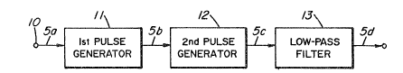
FIG. 4 illustrates a pulse count type FM demodulator,
which is a preEerred embodiment of the present invention.
In FIG. 4, an input terminal 10 is supplied with a
: rectangular signal 5a (FIG. 5A), similar to the rectangular
output Erom the limiter 61 shown in FIG. 1. A first pulse
: generator circuit 11, like the monostable multivibrator 62
of FIG. 1, generates a pulse 5b (FIG. 5B) having a fixed
pulse width commencing at the leading edge of -the
rectangular signal 5a.. The pulse interval ~t of the
lS puise 5b of FIG. 5B is a unction of the input frequency
fin Thus holds the relationship of Equation (3) below:
t T rc .... (3)
A second pulse generator circuit 12, receiViny the
pulse Sb, narrows the pulse width rc f the pulse 5b only
for a period of time proportional to its interval ~ t
(the proportional constant being a, which is a positive
real number), and thereby generates a pulse 5c having a
pulse width f T C - a~ t as shown in FIG. 5C. An LPF 13
integrates the pulse train 5c to provide a demodulated
output, which is represented by Equation (4) below, derived
from Equation (1) above:
.- .
,''~ ' .
,
.
. . . ~
~ ~7~3
-- 7 --
VO = E ~(a ~ c fin ~ a} .... (4)
The characteristic of Equation (4), as shown in ~IG. 6,
indicates a narrower demodulation band on the low frequency
side and, correspondingly, an (a ~ l) times higher
demodulation sensitivity than the F/V characteristic of
the prior art illustrated in FIG. 3. Accordingly, even
where the normalized bandwidth of an FM signal is narrow,
the demodulator is hardly vulnerable to external noise.
FIG. 7 illustrates a pulse count type FM demodulator,
which is another preerred embodiment of the present
invention. In FIG~ 7, a monostable multivibr~tor 21,
serving as a first pulse generator ci.rcuit, generates
pulses 8b ~FIG. 8B) having a pulse width T C commencing
at the l~.~ading and -t~i~i~/edges of~an input rectangular
wave signal 8a to increase the demodulation sensitivity,
and is so adjusted as to keep the ~ t smaller than TC~
The output pulse 8b of the monostable multivibrator 21 is
divided into two branches, of which one is directly fed
to one of the inputs of an AND gate 28 and the other, to
the other input of the AND gate 28 through a delay circuit
29. The delay circuit 29 is comprised of a first
integration circuit comprising a resistor 22 and a
capacitor 23, a ~irst inverter 24 to receive the integrated
output, a second integration circuit which comprises a
resistor 25 and a capacitor 26 and receives the output of
the first inverter 24~ and a second inverter 27 to receive
., ~ .
_;
, : . ,
- - ~ .
, , . . -
-- 8
the output oE this second inteyration circuit. The delay
~ime rl of the delay circuit 29 is set as represented by
Inequality (5) below:
~tmaX C rl~ rc
where ~ tmaX is the pulse interval of the pulse 8b when
the input frequency is at its minimum.
The output 3d of the AND gate 28, as shown in FIGo 8D,
has a pulse width smaller by ~ t than the output pulse 8b
of the monostable multivibrator 21. Integrating the pulse
8d with the LPF 13 gives the F/V characteristic of a = l,
in Flg. 6.
FIG. 9 illustrates an FM demodulator, which is still ~.
another preferred embodiment of the present invention.
In FIG. 9, the output of a monostable multivibrator 21 is
15 the same as that of the correspondlng one in the embodiment
of FIG. 7. Delay circuits 31 to 34 are connected in tandem,
and the respective outputs of -these delay circuits and of
the monostable mu~*ivib:rator 21 are applied to an AND gate
35. For the optimal design, it is recommended to set the
values of the delay time rl of each of the delay circuit
31 to 34 and the number n o:E the delay circuits as
represented by the following Equation-Inequality pair ~6):
T 1 ~ ~ tmax
n rI ~ rc J .~ (6)
The modulation sensitivity of the modulator of FIG. 9,
, '
37~
g
set as described above, is (n ~ 1) times that of the
conventional modulator o FIG. 1.
FIG. 10 illustrates an FM demodulator, which is yet
another preferred embodiment o~ the present invention.
In FIG. 10, the output of a monostable multivibrator 21
is the same as that of the corresponding one in the
embodiment of FIG. 7. A switching circuit 41 is intended
to turn on and off constant current sources 42 and 43.
When an input signal llb is at its "high" level~ the
switching circuit 41 keeps the constant current source 42
on while holding the constant current source 43 off and
open, and vice versa when the input signal llb is at its
"low'l level. Therefore~ when the input llb to the switching
circuit 41 is "high", the constant current source 42 charges
a capacitor ~4 by a high-potential po~er source 48.
Conversely, when the input l].b to the switching circuit 41
is "low", the constant current source 43 discharges the
capacitor 44 to a low-potential power source ~9 (a ground
potential in this particular instance). The higher
potential between the two electrodes of capacitor 44 is
clamped at a fixed potential by a clamp circuit 45.
The relationship o~ Equation ~7) below is to be
maintained between the output current Il of the constant
: current source 42 and the ou-tput current I2 of the constant
current source 43.
I2 nIl (7)
'' ' ,' . - ' ~ ':
.,, ' ~ ': '. "'' '
7~
- 10 -
Since the capaci-tor 44 is charged and discharged by the
constant currents Il and I2, respectively, the inclinations
of its charge and discharge waveforms, shown in FIG. llC,
are constant as represented by Equation (8) below:
dt = c and 2 .... (8)
where c is the capacity of the capacitor 44.
If the upper limit of these charge and discharge
waveforms is clamped at the clamp potential Vc of the clamp
circuit 45, the potential variation ~V ~FIG. llC) during
the period o discharge by the current I2 will be represented
by Equation (9) below:
~V I2
~ = c .... ~g)
where, as is eviclent from FIG. l:lC, ~ t2 equals ~ t.
Therefore, ~-V is given by Equation ~lO) below: -
~V = c2 ~ t .................................... (lO)
Then, the time ~ tl required for returning the
potential variation ~ V to Vc during the period of
discharge by the current Il is calculatecl as follows:
C . o ~ ~ ( 11 )
From Equation (ll), ~ tl _ Ic ~V ............ ~12)
According to Equation (lO), Equation ~12) can be
developed as follows:
.
- :
- . , ~ .:
,. , . . : .
I 1 c
= I2 ~ t 0... (].3)
According to Equation (7), Equation (13~ can be
converted into Equation (14) below:
~tl = n~ t ..................................... (14)
Therefore, by waveform-shaping the charge and
- discharge wavefo:rms shown in FIG~ llC with a reference
voltage obtained from a voltage source 46, which is slightly
lower than the clamp voltage Vc, there is provided a pulse
(FIG, llD) having a width of r c ~ n ~ t. Thus, by varying
the ratio n between the constant currents Il and I2, the
demodula~ion sensitivity can be changed. Integrating the
pulse shown in FIG. llD with the LPF 13 will provide the
desi~ed demodulation output.
FIG. 12 is a more specific circuit diayram of an
integration circuit 100 oE Fig. 10 which comprises the
switching circuit 41, the constant current sources 42 and
43, and the clamp circuit 45. An inpu-t signal llb is
supplied to the base of a first transistor 51 whose emitter
~0 is connected to the emltter of a second transistor 52 and
to a constant current circuit 53. The collector of the
first txansistor 51 is connected to the cathode of a first
diode 54. The base of the second transistor 52 is grounded
through a bias const~nt voltage source 56, and the collector
', ' '' '. ., ' , , ,
7~383
- 12 -
of same is connected to -the cathode of a second diode 55.
The anodes of both the first and second diodes 54 and 55
are connected to a power source. Further, the collectors
of the first and second transistors 51 and 52 are connected
to the bases of third and fourth transistors 57 and 58,
respectively, whose emitters are both connected to the
power source and collectors are connected to those of
fifth and sixth transistors 59 and 5].0, respectively.
The fifth transistor 59, with its collector and base
.. ' lO being short-circuited, is used as a diode, and to their
connecting point is further connected the base of the
: sixth transistor 510, the emitters of both the fifth and
~ sixth transistors being grounded. Being so connected, the
'~ fifth and sixth transistors 59 and 510 serve as a current
mirrox circuit. E'urther, the e~it~er area of the sixth
,' transistor 510 is made n times as yreat as that of the
fifth transistor 59. The collector of the sixth transistor
510 serving as the output point is connected to a irst
terminal of the capacitor 44 whose seaond terrninal is
grounded,. In parallel to the capacitor 44 is connected
a series circuit of a third diode 511 and a reference
voltage source 512.
The above described structure enables the capacitor 44
to be charged and discharged by switching the flrst and
~ 25 second transistors 51 and 52 with the input signal llb and
.' the ratio between the charyiny and discharging currents
,,
' : ': . . ~ . .
~. ~ . ~...... , .
- , ; ' .', : ~. ., '
,: . . . - - :
7~ 3
- 13 -
to be determined by tha-t be-tween the emitter areas of the
fifth and sixth transistors 59 and 510. The third diode
511 and the reference voltage source 512 constitute the
clamp circuit 45, whose clamp value is represented by
Vref ~ Vr, where Vr represents the on-voltage of the diode
511 and Vref, the voltage of the reference voltage source
512.
FIG. 13 shows the F/V characteristics, simulated by
the simulation program of SPICE-F, of an FM demodulator
circuit composed o~ the bipolar transistor circuit
:`
illustrated in FIGS. 10 and 12. The abscissa represents
the frequency, and the ordinate, the D.C. component of the
demodulated output. The characteristics were simulated
with an intermed:iate frequency of 455 kHz, with temperature
variations from -20 to +70 taken lnto consideration.
As is evident froTn these simulated characteristics, a
demodù]ation performance suEficiently close to linearity
can be achieved in the temperature range o~` -20 to ~70
and in the frequency ~f) range of 390 kHz to ~90 kHz.
Inciden~ally, the ratio between the constant currents
Il and I2 is set at 1.75.
As hitherto described~ an FM demodulat~r according
to the present invention makes it possible to increase
the demodula~ion sensitivity. This is achieved by adding
a circuit which subjects the pulse width ~ c of a monostab]e
multivibrator output to pulse width modulation by the pulse
'~
r
: .~
-. . : .
- . . . ,: : .
.. ~ . -
- : - . . , ' ': : :
7~383
- :L~ -
interval ~ t to al-ter the pulse width to r c - aA t.
An FM demodulator according to the invention is especially
suitable for monolithic integration of a demodulator
circuit for use with input signals whose normalized band-
width is comparatively narrow.
c "~,
. - . ' . ' - ',: ' :. , ' '
, :
, , ~ :, :