Note: Descriptions are shown in the official language in which they were submitted.
METHOD & APPARATUS FOR TESTING DI~ITAL SYSTEMS
Field of the Invention
This invention relates to methods and apparatus ~or
testing digital systems ~uch as digital integrated circui.ts
or systems comprising a plurality o~ diyital inteyrated
circuits.
Backyround of the Invention
In one known method for testing large digital
systems such as digital integrated circuits, the elements of
the system are partitioned into combinational networks and
scannable memory elements. The scannable memory elements
have a parallel or normal operation mode in which they are
connected to the combinational networks of the system to
~, provide memory functions required to per~orm the intended
~unctions of the system. The scannable memory elements also
ha~e a serial or scan mode in which they are decoupled from
the combinational logic and connected in series to form a
shift register. Such partitioning and provision of scannable
memory elements is known as Level Sensitive Scan Design
tLSSD).
Digital systems e~ploying LSSD are tested by
configuring the scannable memory elements in serial mode,
shifting a known test stimulus pattern into the shift
register, reconfiguring the scannable memory elements into
parallel mode, runniny the system clock through a sinyle
clock cycle, recon~iguring the scannable memory elements into
serial mode, and shi~ting a test result pattern out o~ the
shift register. The test result pattern is compared with a
calculated test result pattern or with a test result pattern
obtained ~rom combinational loyic known to be ~unctioning
properly to determine whether the combinational logic under
test i5 functioning properly.
Typical LSSD techniques are described in UuS.
Patent No. 3,761,695 issued September 25, 1973 and U.S.
Patent No. 3,783,254 issued January 1, 1974, both in the name
of E.B. Eichelberyer, and in U.S. Patent 4,293,919 issued
~ October 6, 1981 in the names of Dasgupta et al.
', '
, ~
.. ... .- :
. .
The LSSD technique has a numher of ~isadvantayes.
Appropriate test stimulus patterns must be yenerated and
corresponding test result patterns must be calculated or
measured. This requires appropriate alyorithms,
computational facilities and skilled personnel. ~emory must
be provided for storage of test stimulus patterns and
corresponding test result ~atterns until they are required
for test application. Most importantly the scannable memory
elements and the combinational logic to be tested must be
reconfigured after each test stimulus pattern in order to
apply test stimulus patterns and to read out test result
patterns, and the test stimulus patterns and test result
patterns must be transmitted between external test equipment
and the system under test via interconnecting cables which
limit test clock operation to rates lower than the normal
operating clock rate. Consequently, test conditions do not
correspond exactly to normal operating conditions and faults
unique to the normal operating conditions may go undetected.
Moreover, the use of reconfigurable memory elements embedded
throughout the digital system increases design complexity and
cost and compromises the performance of the resulting
system.
In another technique, known as the boundary or
peripheral scan technique, a digital system is partitioned
according to i-ts physi.cal partitioning onto a number of
integrated circuits. A scannable memory element is provided
at each input and output pin of each inteyrated circuit.
These memory elements have a parallel or normal operation
mode in which they connect internal circuitry of the
inteyrated circuits to the input and output pins to permit
normal operation of the integrated circuit. The memory
elements may or may not provide memory functions required in
normal operation of the integrated circuits. The memory
elements also have a serial or scan mode in which they are
decoupled from the internal circuitry of the integrated
circuits and connected in series to ~orm shift registers.
The internal circuitry of integrated circuits
having boundary scan architectures is tested by configuring
:
: '
,
3~
the scannable memory elements in serial mode, shifting a
known test stimulus pattern into memory elements which
correspond to circuit inputs, reconfiguring the scannable
memory elements into parallel mode, runniny the system cloc]c
through a single clock cycle, reconfiguring the scannable
memory elements into serial mode, and shi~ting a test result
pattern out of m~mory elements o-E the boundary register
corresponding to circuit outputs. The test result pattern i5
compared with a calculated test result pattern or with a test
result pattern obtained from an integrated circuit known to
be functioning properly to determine whether the integrated
circuit under test is functioning properly.
External circuitry interconnecting integrated
circuits having boundary scan architectures is tested by
configuring the scannable memory elements of the integrated
circuits into serial mode, shi~ting a known test stimulus
pattern into the scannable memory elements, reconfiguring the
scannable memory elements into parallel mode to interconnect
the outputs of the integrated circuits to the inputs of other
; 20 integrated circuits via the external circuitry, cloc}cing the
memory elements to transfer bits of the test stimulus pattern
over the external circuitry to the inputs of the other
integrated circuit, reconfiguring the scannable memory
elements into serial mode, and shifting a test result pattern
out of the scannable memory elements. The test result
patterns are compared with calculated test result patterns or
test result patterns from integrated circuits haviny
interconnections known to be good to determine whether the
external circuitry is functioning properly.
Boundary scan architectures and techniques may be
combined with LSSD architectures and techni~ues by providing
scannable memory elements at inputs and outputs to the
integrated circuit while also making scannable at least some
of the memory elements which are internal to the integrated
circuit.
Typical boundary scan architectures and techniques
are described in "A Standard Boundary Scan Architecturel',
' ' ' " ,; ' '' ', ' "' ' ~ ' :
-
~ ~7~7~
Version 1.0, Technical Subcommittee of the Joint Tesk ~ction
Group (JTAG), June 19~7.
The boundary scan technique overcomes some of the
problems of the LSSD technique. In particular, the scannable
memory elements are restricted to the periphery of the
functional logic system to be tested, thereby reducing design
complexity and cost. Moreover, the scannable memory elements
are not generally needed for normal operation o~ the
functional logic system and can be bypassed in the normal
operation mode of the systems to avoid compromising
performance of the system in its normal operation mode. The
boundary scan technique also permits relatively
straightforward testing of interconnections between digital
systems.
However, the boundary scan technique does not
overcome the need for generation of appropriate test stimulus
patterns and calculation or measurement of corresponding test
result patterns. Approprîate algorithms, computational
facilities, skilled personnel, and memory for storage of test
stimulus patterns and corresponding test result patterns are
therefore required as in ~SSD techniques. More importantly,
the scannable memory elements must be reconfigured after each
test stimulus pattern in order to apply test stimulus
patterns and to read out test result patterns, and the test
stimulus patterns and test result pa-tterns must be
transmitted between external test equipment and the system
under test via interconnecting cables which limit test clock
operation to rates lower than the normal operating clock rate
as in LSSD techniques. Consequently, the test con-figuration
does not correspond exactly to the normal operation
configuration and certain subtle faults unique to the normal
operation configuration may go undetected.
Built In Self Test (BIST) techni~ues overcome the
need for external test stimulus pattern generation and
storage by providing test stimulus pattern generators and
test result pattern evaluators within the digital system to
be tested. Because the test stimulus patterns and test
result patterns need not be transmitted between external test
:..
.
': '' : ' ' .
, - . . ' ~ '. ' . ' ~'' ; .
': : , : ' . . '
equipment and the system under test via cables, the system
can be teste~ at the normal operating clock rate.
Consequently, faults which appear only a-t high clock rates
will be detected.
For example, Konemann et al, IEEE Journal of Solid
State Circuits, Vol. SC-15, No. 3, pp.31~-319, June 1980
describes the use of linear feeclback shift registers for
generation of pseudo-random test stimulus patterns and for
compression of test result patterns into test result
0 signatures. The pseudo-random test patterns are applied -to
the circuitry under test, and test result patterns are
extracted and accumulated into test result signatures. The
test result signatures are compared to calculated signatures
corresponding to circuitry known to function properly.
Combinations of BIST techniques with LSSD
techniques are described in Krasniewski et al, 24th ACM/IEEE
Design Automation Conference, Paper 24.4, pp.~07~415, June
1987 and Stroud, 25th ACM/IEEE Design Automation Conference,
Paper 3.1, pp.3-8, June 1988. Scannable memory elements of
the circuit to be tested are connected to form a riny
register, and each memory element includes an EXCLUSIVE OR
gate which combines serial and parallel inputs to that memory
element when the memory elements are configured in test mode.
- This arrangement provicles test stimulus pattern generation
and test result pattern compression within the shift
register, thereby avoiding the need for test stimulus pattern
generation and test result pattern compression external to
the shift register as in more typical BIST architectures.
Unfortunately, the scannable memory elements and the
3~ combinational logic to be tested must be reconfigured in
order to apply test stimulus patterns and to read out test
result patterns as in other LSSD techniques. As a result,
test conditions do not correspond exactly to normal operating
conditions and certain faults unique to the normal operating
conditions may go undetected. Moreover, the use of
reconfigurable memory elements embedded throughout the
digital system increases design complexity and cost, and
compromises the performance of the resulting system.
,:, ' . - . , ' . -:
: : .- ' , . ' . : -
. . , . . - , - .
~-q~ 7~
Another example of BIST techniques is described in
U.S. Patent No. 4,357,703 issued November 2, 19~2 in the name
of Nicholas P. Van Brunt. An input shift register anA an
associated generator/accumulator provide a test stimulus
pattern to the circuitry under test, and an output shift
register and an associated generator/accumulator compresses
the corresponding test result pattern into a test result
s~gnature. Interconnections between integrated circuits are
tested by generating test patterns at the output
generator/accumulator of one circuit and compressing
corresponding test result patterns at the input
generator/accumulator of downstream integrated circuits.
~owever, the re~uirement for separate input and output shlft
registers and generator/accumulators complicates
interconnection of the shift registers to the circuitry under
test since the circuit inputs and outputs may typically be
arranged in any order on the periphery of the integrated
circuit.
Summary of the Invention
This invention provides novel methods and apparatus
for testing digital systems which combine advantages of the
techniques described above while avoiding some of their
disadvantages.
One aspect of this invention provides a method and
apparatus for testing a digital system haviny a plurality of
system terminals for coupling input signals into the system
and output signals out of the system during normal operati.on
of the system in which:
at least some of the system terminals are connected
in parallel to boundary register means, the boundary register
means being operable to pass input signals and output signals
transparently through the boundary register means while
accumulating together the input signals and the output
signals;
the state of the digital system and the state of
the boundary register means are initialized to predetermined
states;
-
!
:
'
,
~'rhr3~7~
the digital system and boundary register means are
run through a predetermined number of clock cycles while
passing known input signals through the boundary register
means into the system and the known input siynals and output
signals provided by the digital system are accumulated
together within the boundary reyister means to generate a
test result pattern; and
the generated test result pattern is compared to a
predetermined test result pattern.
The above method and apparatus permits testing of
the digital system in its normal operation mode. Indeed, the
above method and apparatus permit testing of the digital
system while it is connected to other di~ital systems to
receive inputs from and supply outputs to those other digital
systems. Consequently, the digital system can be tested in
its normal operating environment to provide test results
which accurately reflect the operation of the system under
real working conditions. Moreover, the digital system need
not be recon~igured for testing or for normal operation.
The single boundary register means of the above
method and apparatus is connected to input and output
terminals of the digital system in any order. ~here is no
need to separate the input and output terminals and connect
them to separate inp~lt and output registers. This simplifies
physical layout of the digital system and boundary register
means, and simplifies interconnection of the digital system
with the boundary register means.
Another aspect of the invention provides a method
and apparatus for testing a digital system having a plurality
of system terminals for coupling input signals into the
system and output signals out of the system during normal
operation of the system in which:
; at least some of the system terminals are connected
in parallel to boundary register means, the boundary register
means being operable to generate input signals and to pass
said input signals from the houndary register means to
selected system terminals while receiving output signals from
.
.'- , .
" ' , . . ' -' ~ '
~ ': .' ,
*~3~7f~fi
selected system terminals and accumulatlng together the input
signals and the output signals;
the state of the digital system and the state o-f
the boundary register means are initialized to predetermined
states;
the digital system and boundary register means are
run through a predetermined number of clock cycles to
generate input signals and to pass the input signals from the
boundary register means to selected system terminals while
receiving output signals from selected system terminals and
accumulating together within the boundary register means the
input signals and output signals to generate a test result
pattern; and
the generated test result pattern is compared to a
predetermined test result pattern.
The above method and apparatus provide test
generation and accumulation in a single boundary register
means avoiding the need for separate test generators and
accumulators. The single boundary register means of the
` 20 above method and apparatus is connected to input and output
terminals of the digital system in any order simplifying
physical layout of the digital system and boundary register
means and interconnection of the digital system and the
boundary register means.
The above method and apparatus permit testing of
the digital system in isolakion, testing of lnterconnections
between digital systems and combined testing of the digital
system and its connections to other digital systems.
The digital system and the associated boundary
register means may be implemented as a single integrated
circuit. The remaining elements of the test apparatus may
also be implemented as parts of the same integrated circuit.
A plurality of digital subsystems may be
interconnected via boundary registers surrounding individual
subsystems to provide a partitioned systenl having integral
self-test functions. The system may implemented as a single
integrated circuit or may be partitioned on a subsystem basis
into separate integrated circuits.
. ~
:.
.
- ,
,, , . :: :
. : .
' ' ' ' '' ' :
~"~r,,.~
Other aspects of the invention include the novel
boundary registers of the test apparatus descri~ed above and
novel unidirectional and bidirectional boundary reg:ister
cells which may be used to implement such boundary registers.
Brief Description of the Drawings
Embodiments of the invention are described below by
way of example only with reference to the accompanyiny
drawings in which:
Figure 1 is a schematic Aiagram of kest apparatus
according to an embodiment of the invention;
Figure 2 is a schematic diagram of a boundary
register of the test apparatus of Figure l;
Figure 3 is a schQmatic diagram of one
implementation of a unidirectional cell of the boundary
register of Figure 2;
Figure 4 is a schematic diagram of one
implementation of a bidirectional cell of the boundary
register of Figure 2;
: Figure 5 is a schematic diagram of the boundary
~: 20 register cells of Figures 3 and 4 interconnected to form part
of a boundary register;
Figure 6 is a schematic diagram of the boundary
~ register part of Figure S configured for shi~ting test
:~ patterns into and out of the boundary register;
Figure 7 is a schematic diagram of the boundar~
register part of Figure 5 configured for mission mode
testing;
Figure 8 is a schematic diagram of the boundary
register part of Figure 5 configured for internal mode
testing;
Figure 9 is a schematic diagram of the boundary
register part of Figure 5 configured for external mode
testing; and
Figure 10 is a schematic diagram of a digital
~; 35 system incorporating the test apparatus illustrated in Figure
:
.
.:'',' . ,, ' . :
: ~ ' , . ' .
- :
.
~ . .
3tj~
Detailed Description of Embodiments
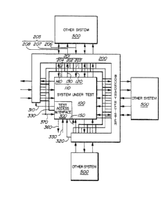
Figure 1 illustrates test apparatus for testing a
digital system loo having a plurality of system terminals llo
for coupling input signals into the system lO0 and output
signals out of the system 100 during normal operation of the
system lO0. The system terminals 110 include input terminals
120, output terminals 130 and bidirectional terminals 140.
The system 100 also has a system clock terminal 150.
The test apparatus comprises boundary register
means in the form of a boundary register 200 for connection
in parallel to each of the system terminals 110. The
boundary register 200 has a first plurality of kerminals 201
for connection to corresponding terminals 110 of the system
100 under test and a second plurality of terminals 205 for
connection to corresponding terminals of external systems
500. The terminals 201, 205 include input terminals 202,
206, output terminals 203, 207, and bidirectional terminals
: 204, 208. The external systems 500 may be systems normally
connected to the system 100 for normal operation of the
system 100, or external test systems connected to the system
100 via the boundary register 200 only to provide inputs and
~ receive outputs during testing.
.~ The test apparatus further comprises a test access
interface 300 which is connected to the boundary register 200
by méans of a serial data input line 310 for coupling serial
data from the test access interface 300 to the houndary
~ register 200 and by means of a serial data output line 320
for coupling serial data from the boundary register 200 to
the test access interface 300. The test access interface 300
is also connected to the boundary register 200 by means of a
mode control bus 330 for coupling mode control signals to the
boundary re~ister 200.
The test access interface 300 has a serial data
input terminal 350 for receiving serial data and control
signals from external test equipment, and a sexial data
output terminal 360 for sending serial data to external test
equipment, and a test clock terminal 370 for receiving timing
information from external test equipment.
. --, , .
, ', ,, ~ ' ' ' ': '
. :' ' . . ' : , ,
,
:
-: - . .
~ ~7~3~4i
11
In use of the test apparatus in one test mode, the
test access inter~ace 300 applies a mode control signal on
the mode control bus 330 to configure the boundary register
200 in scan mode and connects the serial data input terminal
350 to the serial data input line 310. The boundary register
200, which is operable as a shift register when configured in
scan mode, is clocked to shift a predetermined seed pattern
into the boundary register 200 to initialize the state of the
boundary register 200. The test access interface applies a
reset condition or other initialization sequence to the
: system 100 under test and to any external systems 500
connected to the system 100 via the boundary register 200.
The test access interface applies another mode
control signal on the mode control bus 330 to reconfigure the
boundary register 200 for mission mode testing and connects
the register serial data input line 310 to the reyister
serial data output line 320. When configured for mission
mode testing, the boundary register 200 is operable to pass
input signals and output signals transparently through the
boundary register 200 while accumulating together the input
signals and the output signals within the boundary register
200. The system 100 under test and the boundary register 200
are run through a predetermined number o~ clock cycles while
passing known input signals through the boundary register 200
into the sys~em 100 under test and accumulating together
within the boundary register 200 the known input signals and
output signals provided by the system 100 under test to
generate a test result pattern.
The known input signals may be provided by external
test equipment or may be provided by other d.igital systems
connected to the system 100 under test via the boundary
register 200. In the latter case, the system 100 is tested
in its normal operating environment and ~aults unique to
operation of the system 100 in its normal operating
environment may be detected.
The test access interface 300 applies another mode
control signal to the mode control bus 330 to reconfigure the
boundary register 200 in scan mode and connects the serial
- ~ '
'
~J~r~7~3~3~
data output line 320 to the serial data outpuk terminal 360.
The boundary register ~oO is clocked to shi~t the test result
pattern out of the boundary register 200 for comparison with
a predetermined test result pattern obtained ~rom or
calculated for a properly functioning system.
In use of the test apparatus in other test modes,
the states o~ the boundary register 200 and the system ~00
under test are initialized as described above but different
mode control signals are applied to the mode control bus 330
to render the boundary register 200 operable to generate
input signals and to pass those input signals from the
boundary register 200 to selected system terminals 110 while
receiving output signals from selected system terminals 110
and accumulating together the input signals and the output
signals within the boundary register 200. In these other
test modesl the test access interface 300 connects the serial
data input line 310 to the serial data output line 320 to
. configure the boundary register 200 as a ring register.
Inputs to the boundary register 200 from external
test equipment or from other digital systems 500 connected to
the system 100 under test via the boundary register 200 may
or may not be used in the generation oE input signals by the
~ boundary register 200 as will be described in greater detail
below with reference to a particular implementation o~ the
boundary register 200. In an "internal test mode" described
: in greater detail below, inputs from other digital systems
500 are not used to generate test inputs to the system 100
;. under te~t, and the system 100 is tested in isolation. In an
"external test mode" described in greater detail below,
inputs from other digital systems 500 and outputs to other
digital systems 500 are used to generate test inputs to the
system 100 under testl so the system 100 and the external
systems 500 are tested together along with the
interconnections between the systems 100l 500.
In the particular implementation of the boundary
~. register 200 described below, the boundary register 200 is
; operable to pass the output signals received from selected
terminals of the system 100 under test transparently through
~'
,:~
:, .
.
- ' :. .
,
~ ~s~7~
the boundary register 200 while accumulating those output
signals toyether with the input signals generated by the
boundary register 200. This feature is particularly useful
for testin~ two or more interconnected digital systems 100,
500 as will be described in greater detail below.
ReEerring to Figure 2, one implementation of the
boundary register 200 comprises a plurality of unidirectional
boundary register cells 210 each having a parallel input
terminal 212, a parallel output terminal 213, a serial input
terminal 214, a serial output terminal 215, a pair of mode
control terminals 216, 217 and a test clock terminal 218.
The terminals 212 - 218 are connected to signal gating and
accumulation circuitry 220 described in greater detail below.
Some of the unidirectional boundary register cells
210 have their respective parallel output terminals 213
connected to respective input terminals 120 of ~he system 100
under test for coupling inputs to the system 100 and their
mode control terminals 216, 217 connected to selected lines
331, 332 of the mode control bus 330. These cèlls pass
signals from the boundary register 200 into the system 100
under test and are referred to as input cells 230 in the
description which follows. Others of the unidirectional
boundary reyister cells 210 have their respective parallel
input terminals 212 connected to respective output terminals
120 o~ the system 100 under test for receiving outputs from
the system 100 and their mode control terminals 216, 217
connected to other selected lines 333, 334 of the mocle
control bus 330. These cells receive outputs from the system
100 under test and are referred to as output cells 240 in the
description which follows.
In the implementation of Figure 2, the boundary
register 200 further comprises a plurality of bidirectional
boundary register cells 250, each having first and second
bidirectional or parallel input/output terminals 252, 253, a
; 35 serial input terminal 254, a serial output terminal 255, four
mode control terminals 256, 257, 258, 259, a direction
control terminal 260 and a test clock terminal 261. The
- : .
'
: : . ,
3~7~$~i
1~
terminals 252 - 261 are connected to signal gatiny and
accumulation circuitry 270 described in greater detail below.
Each bidirectional cell 250 has one of its parallel
input/output terminals 252, 253 connected to a respective
bidirectional terminal 140 of the system 100 under test and
its direction control terminal 260 connected to a terminal
160 which carries a signal which controls the direction of
the respective bidirectional terminal 140. The four mode
control terminals 256 - 259 of each bidirectional cell 250
are connected to the four lines 331 - 334 of the mode control
bus 330. The bidirectional cells 250 are able to pass inputs
into the system lO0 and receive outputs from the system 100
according to the logical value applied to the direction
control terminal 260.
The input cells 230, output cells 240 and
bidirectional cells 250 are connected in series, serial
output terminals 215, 255 to serial input terminals 214, 254
to comprise a chain of cells. The cells may be connected in
any serial order and, for a given system 100 under test, are
connected in an order which corresponds to the arrangement of
input terminals 120, output terminals 130 and bidirectional
terminals 140 so as to simpli~y interconnection of the system
100 wi~h the boundary register 200.
Referring to Figure 3, in one implementation o~ the
25 unidirectional cells 210, the mode control terminals 216, 217
comprise an input select terminal 216 and an output select
terminal 217. In this implementation, the signal gating and
: accumulation circuitry 220 comprises an AND gate 221 having a
first input connected to the input select terminal 216 and a
second input connected to the paralleI input terminal 217.; an
EXCLUSIVE OR gate 222 having a first input connected to the
output of the AND gate 221 and a second input connected to
khe serial input terminal 214; a flip flop 223 having a data
input connected to the output of the EXCLUSIVE OR gate 222, a
clock input connected to the clock terminal 218 and a data
output connected to the serial output terminal 215; and a
multiplexer 224 having a first data input connected to the
data output of the flip flop 223, a second data input
. ' .
' .' , , .
- :
- ' ., ' ' . '' '
~ ~,s.~ fi
connected to the parallel input terminal 212, a select input
connected to the output select terminal 217 and a data output
connected to the parallel output terminal 213.
The unidirectional cell 210 shown in Fiyure 3 has
four distinct modes o~ operation depending on the value of
siynals applied to the input and output select terminals 216,
217. When a logical zero is applied to both the input select
terminal 216 and the output select terminal 217 the
unidirectional cell 210 transfers one bit from the parallel
input terminal 212 to the parallel output terminal 213 and
transfers when clocked another bit from the serial input
terminal 214 to the serial output terminal 215. When a
logical one is applied to the input select terminal 216 and a
logical zero is applied to the output select terminal 217 the
unidirectional cell 210 transfers a bit from the parallel
input terminal 212 to the parallel output terminal 213 while
transferring when clocked the modulo 2 sum of bits on the
parallel input kerminal 212 and the serial input terminal 21
to the serial output terminal 215. When a logical zero is
applied to the input select terminal 216 and a logical one is
applied to the output select terminal 217, the unidirectional
- cell 210 transfers when clocked a blt from the serial input
termi.nal 214 to both the serial output terminal 215 and the
parallel output terminal 213. When a logical one is applied
to both the input select terminal 216 and the output select
terminal 217 the unidirectional cell 210 transfers the modulo
2 sum of bits on the parallel input terminal 212 and the
serial input -terminal 214 to both the parallel output
terminal 213 and the serial output terminal 215.
Referring to Figure 4, in one implementation of the
bidirectional cells 250, the mode conkrol terminals 256 -259
comprise first and second input select terminals 256, 257,
and first and second output select terminals 258, 259. In
this implementation, the signal gating and accumulation
circuitry 270 comprises a first AND gate 272 having a first
input connected to the first input select terminal 256, a
second input connected to the first parallel input/output
te~minal 252, and a third input connected to the direction
-
. : . ~ ,
- , ' ' ' :. ' ' '
: ~ , . ...
,
.
,
'~
16
select terminal 260; an invertor 273 having an inæut
connected to the direction select terminal 260; a second AND
gate 274 having a first input connected to the second input
select terminal 257, a second input connected to the secon~
parallel input/output terminal 253 and a third input
connected to the output of the invertor 273; an OR gate 275
having a first input connected to the output of the first AND
gate 272 and a second input connected to the output of the
second AND gate 274; an EXCLUSIVE OR gate 276 having a first
input connected to the output of the OR gate 275 and a second
input connected to the serial input terminal 254; a flip flop
277 having a data input connected to the output of the
E~CLUSIVE OR yate 276, a clock input connected to the clock
terminal 261 and a data output connected to the serial output
terminal 255; a first multiplexer 278 having a first data
input connected to the data output of the flip flop 277, a
second data input connected to the first parallel
input/output terminal 252 and a select input connected to the
first output select terminal 258; a first tri-state buffer
279 having an enable input ccnnected to the direction select
terminal 260, a data input connected to data output of the
first multiplexer 278 and a data output connected to the
second parallel input/output terminal 253; a second
multiplexer 280 having a first data input connected to the
data output of the flip flop 277, a second data input
connected to the second parallel input/output terminal 253
and a select input connected to the second output select
terminal 259; a second tri-state buffer 281 having an enable
input connected to the output of the invertor 273, a data
input connected to data outpuk of the second multiplexer 280
and a data output connected to the first parallel
input/output terminal 252.
The bidirectional cell 250 has one set of four
modes in which the first input select terminal 256
corresponds to the input select terminal 216 of the
unidirectional cell 210, the ~`irst output select terminal 258
corresponds to output select terminal 217 of the
unidirectional cell 210, the first parallel input/output
- : :
,
B6
terminal 252 corresponds to the parallel input terminal 212
of the unidirectional ce].l 210 and the second parallel
input/output terminal 253 corresponds to the parallel output
terminal 213 of the unidirectional cell 210, and another set
of four modes in which the seconcl input select terminal 257
corresponds to the input select terminal 216 of the
unidirectional cell 210, the second output select terminal
259 corresponds to the output select terminal 217 of the
unidirectional cell 210, the second parallel input/output
: 10 terminal 253 corresponds to the parallel input terminal 212
of the unidirectional cell 210 and the first parallel
: input/output terminal 252 corresponds to the parallel output
terminal 213 of the unidirectional cell 210. The first set
of modes is selected by applying a logical zero to the
direction select terminal 260 and applying mode control bits
to the first input and output select terminals 256, 25~ as
; described above for the input and output select terminals
.~ 216, 217 of the unidirectional cells 210. The seeond set of
modes is seleeted by applying a logieal one to the direetion
seleet terminal 260 and applying mode eontrol bits to the
seeond input and output seleet terminals 257, 259 as
deseribed above for the input and output seleet terminals
216, 217 of the unidirectional cells 210.
The unidirectional and bidirectional cells 210, 250
are connected as shown in Figure 5 to eonstruct part of the
boundary register 200.
A unidirectional cell 210 is configured as an input
eell 230 by eonnecting its parallel input terminal 212 to
;- external test e~uipment or to another digital system 500, its
- 30 parallel output terminal 213 to an input terminal 120 of the
: system 100 to be tested, its serial input terminal 214 to the
serial output terminal of a preceding cell (not shown), and
its serial output terminal 215 to the serial input terminal
254 of a succeeding cell 250. The input and output select
: 35 terminals 216, 217 are eonneeted to leads 332, 331
respeetively of the mode control bus 330, and the test clock
terminal 218 is eonnected to a test clock line 371.
~. , ' '
' ', ~ ,' ' ', . ~
,
,
~r~
18
Another unidirectional cell 210 is configured as an
output cell 2~0 by connecting its parallel input terminal 212
to an output terminal 130 of the system loo to ~e tested, its
parallel output terminal 213 to external test equipment or
another digital system 500, its serial input terminal 214 to
the serial output terminal 255 of a preceding cell 250 and
its seri.al output terminal 215 to the serial input terminal
of a succeeding cell (not shown). The input and output
select terminals 216, 217 are connected to leads 33~, 333
respectively of the mode control bus 330, and the test clock
terminal 218 is connected to the test clock line 371.
A bidirectional cell 250 is connected between the
input cell 230 and the output cell 240 by connecting one of
its parallel input/output terminals 252 to a bidirectional
15 terminal 140 of the system 100 under test and the other
parallel input/output terminal 253 to external test equipment
or another digital syst~m, connecting its serial input
terminal 254 to the serial output terminal 215 of the
preceding cell 230 and connecting its serial output terminal
20 255 to the serial input terminal 214 of the succeeding cell
240. The first and second i.nput select terminals 256, 257
and the first and second output select terminals 258, 259 are
connected to leads 331 - 334 respectively of the mode control
bus 330, and the test clock input terminal 261 is connected
to the test clock line 371. The direction control ter~ina].
is connected to a terminal 160 of the system 100 under test
which controls the direction of the bidirectional terminal
140.
T~e input cells 230, output cells 240 and
bidirectional cells 250 may be arranged in any order to form
the boundary register 200 and are generally arranged in an
order corresponding to the physical arrangement of input,
output and bidirection terminals 120, 130, 140 of the system
100 to be tested so as to facilitate interconnection of the
35 boundary register 200 and the system 100.
The operating mode of the boundary register 200 is
controlled by signals applied to the mode control bus 330.
. Figure 6 illustrates the signal paths for the shift mode of
. .
, ~ ': ' , . " .
3~
lg
the boundary register 200 which is obtained by applyiny
logical zeros to each lead 331 - 334 of the mode control bus.
In the shift mode the boundary reyister 200 shifts bits
serially without alteration. This mode is useful ~or
shifting test stimulus or seed patterns into the boundary
register 200 and for shi~tiny test result patterns out of the
boundary register 200. The boundary register 200 also passes
parallel data transparently in this mode of opèration.
Conse~uently this mode can be used during normal operation of
the system 100 in conjunction with other digltal systems 500
connected to the system 100 via the boundary register 200.
The bidirectional cell 250 is shown operating as an output
cell since a logical one is applied to the direction select
terminal 260.
Figure 7 illustrates the signal paths for the
mission mode of the boundary register 200 which is obtained
by applying logical zeros to leads 331, 333 and logical ones
to leads 332, 334 o~ the mode control bus, and connecting the
serial output line 320 to the serial input line 310 at the
test access interface 300 to configure the boundary register
200 as a ring register. In the mission mode each cell 230,
240, 250 of the boundary register passes parallel data
transparently while applying the modulo 2 sum of the serial
input data and the parallel input data to the serial output
terminal 215, 255. Thus, the boundary register 200 passes
inputs and outputs transparently into and out of the system
100 under test while accumulatiny the inputs and outputs in a
running checksum which can be compared to a kncwn checksum to
determine whether the system 100 under test is fllnctioning
properly. Because the boundary register 200 passes inputs
and outputs transparently in this mode, the system 100 can be
connected to external systems 500 via the boundary register
200 for normal operation, and its normal operation can be
monitored without perturbation.
Figure 8 illustrates the signal paths for the
internal test mode o~ the boundary register 200 which is
obtained by applying logical zaros to leads 332, 333 and
logical ones to leads 331, 334 of the mode control bus 330,
:"
' . .
~ . . -
'
7~4~;
and connecting the serial output line 320 to the serial input
line 310 at the test access interface to confiyure the
boundary register 200 as a riny register. In the internal
test mode, input cells 230 and bidirectional cells operatiny
as input cells (not shown) do not trans~er parallel inputs to
the corresponding input terminals 120 of the system 100 under
- test. Instead the input cells 230 transfer serial data to
the input terminals 120. Output cells 240 and bidirectional
cells operating as output cells (such as cell 250 shown in
Figure 8) transfer the modulo 2 sum of serial input data and
parallel data received ~rom output terminals 130 o~ the
system lOo under test to serial output terminals 215, 25~.
~hus, the boundary register 200 isolates the system 100 under
test from external systems 500 while accumulating the outputs
in a running checksum which can be compared to a known
checksum to determine whether the system 100 under test is
functioning properly. Moreover, because the accumulated
checksum is trans~erred to the system 100 under test during
subsequent clock cycles, the boundary register 200 acts as a
test input generator as well as a test result accumulator in
this test mode. The connection of the serial input line 310
to the serial output line 320 provides further feedback for
generation purposes.
Figure 9 illustrates the signal paths ~or the
external test mode of the boundary register 200 obtained by
applying logical ones to all leads 331 ~ 33~ o~ -the mode
control bus 330 and connecting the serial output line 320 to
the serial input line 310 at the test access interface 300 to
con~igure the boundary register 200 as a ring register. In
the external test mode, a~1 cells 230, 240, 250 trans~er when
clocked the modulo 2 sum of the parallel input data and the
serial input data to both the parallel output terminals 213,
253 and the serial output terminals 215, 255. Thus, the
boundary register 200 generates inputs to the system lO0
under test and outputs to external systems 500 connected to
the system 100 via the boundary register while accumulating
those inputs and outputs in a running checksum. Because the
running checksum depends on the operation o~ systems external
:
.' ' .
~ ~r~
to the system 100 as well as the operation of the system 100,
it can be compared with known checksums to simultaneously
test the operation of the system 100, external systems 500
connected to the system 100 via the boundary reyister 200 and
interconnections between the syste~ 100 and those external
systems 500.
The boundary register 200 may be conflgured in
numerous other test modes by application of other
combinations of logical values to leads 331 - 334 of the mode
control bus 330.
The digital system 100 and its associated boundary
register 200 may be implemented as a single integrated
circuit with the boundary register 200 connected in parallel
between input and output terminals of the integrated circuit
and corresponding input and output terminals 110 of the
system 100. Such an integrated circuit is readily tested by
application of appropriate input signals to configure and
initialize the boundary register 200, run the boundary
register 200 and system 100 through a predetermined number of
clock cycles, and read out test result patterns for
comparison with known test result patterns. The integrated
circuit can be tested in isolation or in situ on a printed
circuit board connected to other inteyrated circuits.
The input signals required for configuring and
initializing the boundary register 200 and for reading out
test result patterns may be supplied by an external test
access interface 300, or the test access interface 300 may be
implemented as part o~ the same integrated circuit.
The digital system 100 may be partitioned into a
plurality of subsystems lOOA, lOOB, 100c, each with an
associated boundary register 200A, 200B, 200C. The
subsystems lOOA, lOOB, 100c are interconnected via -the
boundary registers 200A, 200B, 200C as shown in Figure 10.
Each subsystem lOOA, lOOB, 100c may also include an
35 associated test access interface 300A, 300B, 300C.
Alternatively, a single test access interface may be
provided, and the boundary registers 200A, 200~r 200C may be
, , ' : ~ . , :
,' ~ ' , . .
.
: ~
connected in series to form a single boundary register
controlled by the single test access interface.
Numerous modifications of the embodiment described
above are wlthin the scope of the invention as claimed below.
For example, where the digital system 100 to be
tested has no bidirectional terminals 140, the boundary
register 200 may be implemented with only unidirectional
cells 210 configured as input cells 230 and output cells 240
as required. Alternatively, a progra-mmable boundary register
200 comprising only bidirectional cells 250 may be supplied
as part of external test equipment for connection to a wide
variety of systems 10~ to be tested. Such a boundary
register 200 could be programmed by means of appropriate
signals on the direction select terminals 260 of the
individual cells 250 to correspond to the particular pattern
of input and output terminals 120, 130 for the particular
system 100 under test.
Not all of the system terminals 110 need be
connected to the boundary register 200 if monitoring of only
some of the system inputs and oukputs is desired.
The serial input line 310 need not be connected to
the serial output line 320 to form a ring register in the
various test modes described above. However, if the boundary
~ register 200 is not configured as a ring register, a known
; 25 signal must be applied to the serial input line 310, and the
generation and accumulation characteristics of the boundary
register 200 will be altered.
Other implementations of boundary register cells
- providing similar functionality are possible and will be
apparent to those skilled in the design of test systems and
circuitry.
Linear feedback paths may be provided between
~ selected cells of the boundary register 200 in certain test
`~ modes to modify the generation and accumulation
characteristics of the boundary register 200 in those test
modes.
The boundary reg7ster may be configured for
parallel loading rather than serial loading as described above.
.' : -
,