Note: Descriptions are shown in the official language in which they were submitted.
The present invention generally relates to
microstrip antennas for transmi~ting and/or receiving radio
frequency signals, and more particularly, to techniques for
broadening and optimizing microstrip antenna bandwidth.
Still more particularly, the present invention relates to
broadband microstrip antennas having stacked passive and
driven elements.
Both the prior art and the present invention will be
described in conjunction with the accompanying drawings in
which:
Figure 1 is a side view in cross-section of a prior
art thick substrate microstrip patch;
Figure 2 is a side view in cross-section of a prior
art single capacitively coupled microstrip radiator element;
Figure 3 is an elevated side view in perspective and
partial cross-section of a prior art stacked microstrip
antenna structure;
Figure 4 is a side view in cross-section of a
presently preferred exemplary embodim~nt of khis invention;
Figure 5 is an exploded side view in perspective of
the embodiment shown in Figure 4;
Figure 6A is a side view in cross-section of a
simple microstrip element;
Figure 6B is a schematic diagram of a two-port RLC
circuit equivalent to the microstrip element shown in Figure
6A;
Figure 7 is a graphical illustration of the
rn/
.~ . .
individual theoretical overlappîng resonances of the antenna
structure elements shown in Figure 4;
Figure 8 is a graphical illustration of the
composite re onance of the structure shown in Figure 4;
Figure 9 is a schematic diagram of the lump-
- component equivalent circuit for the antenna structure shown
in Figure 4;
Figure 10 i8 a schematic diagram of the antenna
structure shown in Figure 4 showing inter-element
capacitances;
Figure 11 is a schematic illustration o~ the
effective inter-element capacitances which exist in the
antenna structure shown in Figure 4 at some low frequency FLoW
within the antenna operating frequency range;
Figure 12 is a schematic illustration of the
effective inter-element capacitances existing in the antenna
structure shown in Figure 4 when the antenna structure is
operated at some mid frequency FMID approximately at the
middle of its operating frequency range;
Figure 13 is a schematic illustration of the
effective inter-element capacitances existing in the antenna
structure shown in Figure 4 when the antenna structure is
operated at some high frequency FHIGH near the upper end of
its operating frequency range; and
Figure 14 is a graphical illustration of the gain
versus frequency response plot of the antenna structure shown
in Figure 4.
rn/~,~J
.
.... . . . . .. .. .
- ~ ,, . ~ ' . '
-
' ' , ~ ,
Microstrip antennas of many types are now well-known
in the art. Briefly, microstrip antenna radiators comprise
resonantly dimensioned conductive surfaces disposed less than
about one-tenth of a wavelength above a more extensive
underlying conductive ground plane. The radiator elements
may be spaced above the ground plane by an intermediate
dielectric layer or by suitable mechanical standoff posts or
the like. In some forms (especially at higher ~requencies,
such as UHF), the microstrip radiators and interconnecting
1~ microstrip RF feedline structures are formed by photochemical
etching techniques (like those used to form printed circuits)
on one side of a doubly clad dielectric sheet, with the other
side of the sheet providing at least part of the underlying
ground plane or conductive reference surface.
Microstrip radiators of many types have become quite
popular due to several desirable electrical and mechanical
characteristics. However, microstrip radiators naturally
tend to have relatively narrow bandwidths (e.g., on the order
of 2-5~ or so). This natural characteristic sometimes
~0 presents a considerable disadvantage and disincentive to th~
use of microstrip antenna system
For example, there is considerable demand for
antennas in the L-band frequency range which covers both of
the global positioning satellite (GPS) frequencies Ll (1575
MHz) and L2 (1227 MH2). It may also be desirable to include
the L3 frequency (1381 MHz) to enable the system to be used
in either a global antenna system (GAS) or in G/AIT IONDS
rn/~
~ .
`' ` ~.28~L7
program. As may be appreciated, i~ a single antenna system
is to cover both bands Ll and L2, the required bandwidth is
on the order of at least 25~ (e.g/, ~F divided by the
midpoint frequency).
Although microstrip radiating elements have many
characteristics (e.g., physical ruggedness, low cost, and
small size) that might make them attractive ~or use in such a
medium bandwidth situation, available operating bandwidths
for a given microstrip antenna radiator have typically been
much less than 25~ -- even when ~broadbanded~ by use of prior
art techniqu~s.
Various ways to "broadband" a microstrip antenna
assembly are known. For example, applicant's U.S. Patent No.
4,835,539 issuad May 30, 1989 discloses a microstrip antenna
which is broadbanded by optimizing the inductive and
capacitive reactances of the antenna feedline.
Previous attempts at producing a broadband
microstrip antenna array element generally followed two basic
approaches: (1) the thick substrate microstrip patch; and (2)
the single capacitively-coupled resonator radiator.
The thick substrate microstrip patch 10 (shown in
prior art Figure 1) includes a relatively thick dielectric
substrate 12 which separates the patch ground plane 14 from
the radiating patch 16 ~and thus defines a cavity of
relatively large dimension between the two patches). A
coaxial feedline connection 18 has its ground conductor
connected to ground plane patch 14 and its center conductor
rn/
: .: . . . .
.
'' " ' '`
:. ~ , . . .
287917
connected to patch feed pin(s) 20. Feed pin(s) 20 pass
through substrate 12 and conduct RF between connection 18 and
radiating patch 16.
The thick substrate patch shown in Figure 1 has a
practical maximum bandwidth of 12~-15% at 2.0:1 ~SWR (voltage
standing wave ratio). In order to achieve this bandwidth
performance, however, two feed pins 20a and 20b are required
to ensure cancellation of the cross-polarized component and
maximize radiation efficiency. Inclusion of these
r ~ ~
... .
~7~9~
feed pins 20 (and associated required pha~ing
circuitry 22) severely limits the practical use of
the thick substrate patch design in antenna arrays,
since the fabrication process is complicated, and
structural strength and reliability are
compromised.
Concerns over reliability and production
cost rule out the use of the feedthroughs necessary
for thick substrate elements, at least for antenna
structures which are to be mass produced and/or used
in harsh environments or critical applications.
Dual linear or circularly polarized operation of
thick substrate elements aggravates these cost and
reliability problems, since an orthogonal pair of
feed connections are required -- resulting in a
total of four feed pins per patch.
The single capacitively coupled element 30
shown in prior art FIGURE 2 eliminates the need for
direct feedthrough connections. The driven patch 32
is fed by microstrip circuitry (not shown) printed
on the driver substrate 34 and directly connected to
the driven patch. Energy radiated by driven patch
32 excites a parasitic element 36 separated from the
driven patch by a foam dielectric spacer 38.
Parasitic element 36 and driven patch 32 have
slightly different resonant frequencies -- resulting
in a broadbandinq effect.
The structure shown in FIGVRE 2 has a
bandwidth which is comparable to that of the
structure shown in FIGURE 1, is very easy to
.
2879~'7
,8
fahricate (for example, the three layers may be
laminated together), and is al80 easily adapted to
varying polarization re~uirements. Unfortunately,
the maximum bandwidth of the FIGURE 2 structure is
only about 14% at 2:1 VSWR. While this bandwidth is
sufEicient for certain applications, greater
bandwidth is often required.
It is possible to increase the bandwidth
of the structure shown in FIGURE 2 to up to about
18% bandwidth by providing l/2 wavelength matching
stubs. Unfortunately, the matching circuitry takes
up a substantial amount of substrate real estate,
increasing the size of the antenna structure.
Moreover, the average VSWR of such a structure has
been calculated and experimentally verified to be
about 1.9:1 -- which is too high for the output
stages of many RF transceivers and also results in
inafficiency due to excessive transmission line
return loss.
Some non-exhaustive examples of prior art
techniques for achieving a broadened bandwidth
microstrip antenna are illustrated by the following
prior issued United States patents:
U.S. Patent Re 29,911 - Munson et al (1979)
U.S. Patent 4,070,676 - Sanford (1978)
U.S. Patent 4,180,817 - Sanford (1979)
U.S. Patent 4,131,893 - Munson et al (1978)
U.S. Patent ~,160,976 - Conroy (1979)
U.S. Patent 4,259,670 - Schiavone (1981)
U.S. Patent 4,320,401 - Schiavone (1982)
--
~.2~379~7
U.S. Patent 4,329,689 - Yee (1982)
U.S. Patent 4,401,988 - Kaloi (1983)
U.S. Patent 4,445,122 - Pues (1984)
U.S. Patent 4,477,813 - Weiss (1984)
U.S. Patent 4,529,987 - Bhartia et al (1985)
See also Sanford, "Advanced Microstrip
Antenna Development", Volume I, Technoloqv Studies
For Aircraft Phased Arrays, Report No.
FAA-FM-80-11-Vol-1; TSC-FAA-80-15-Vol-1 (June, 1981).
As discussed in some o~ the prior art
references cited above -- particularly in
commonly-assigned U.S. Patent No. 4,070,676 to
Sanford -- the typical 2-5% natural bandwidth of a
microstrip radiator can be increased somewhat by
stacking multiple radiators of various sizes above
the ground plane parallel to one another and
parallel to the ground plane. In one embodiment
disclosed in the Sanford patent (and shown ln prior
art FIGURE 3 of the subject application), elements
40,42 of different sizes are spaced apart from the
ground plane surface 44 (and from one another) by
layers of dielectric material 46,48. The largest
element 40 is located nearest the ground plane, with
successively smaller elements being stacked in the
order of their resollant frequencies.
The topmost of Sanford's elements~42) is
driven with a conventional microstrip-feedline 50,
while element 40 disposed between the topmost
element and the ground plane remains passive.
Mutual coupling of energy between the resonant and
2879~7
- . jr
non-resonant elements causes the paraaitic elements
to act as extensions of the ground plane and/or
radio frequency feed means. The resulting compact
multiple resonant radiator exhibits a potentially
large number of multiple resonances with very little
degradation of efficiency or change in radiation
pattern.
Others have also designed stacked
microstrip antenna structures. For example, the
Kaloi patent discloses a coupled multilayer
microstrip antenna having upper and lower elements
tuned to the same frequency in an attempt to provide
enhanced radiation at angles closer to the ground
plane.
The Yee patent discloses a broadband
stacked antenna structure having three discoid
elements stacked above a ground plane in order of
decreasing size. A coaxial cable center conductor
is electrically connected to the top conducting
plane. Yee also provides openings through his
intermediate elements (supposedly to increase
coupling o energy between the stacked elements).
The Yee patent claims tllat the bandwidth of this
structure is "at least as great as 6%, and possibly
higher, even up to 10%." As can be appreciated,
this bandwidth is insufficient for many applications.
It would be highly desirable to produce a
rugged, e~ficient, easy to fabricate, broadband,
dual linearly polarized, microstrip antenna array
element that does not require a separate impedance
` ` i lZ8791~ ~
/ l~
matching circuit or feedthrough connections between
layers, and yet provides a 2.0:1 VSWR bandwidth of
at least 18%.
S~MMARY OF T~E INVENTION
The present invention provides a composite
structure antenna element including stacked
radiators which may be etched on low loss microwave
substrates. Broadband impedance and radiation
characteristics are obtained by using three or more
microstrip patch elements that have individual
resonances which are slightly offset from one
another. Substrate thicknesses and radiation
resonances are selected to provide an average input
VSWR from 1.4:1 to 2.0:1 (18% bandwidth to 25%
bandwidth, respectively).
The antenna structure provided by the
invention is easy to fabricate, requires no
feed-through connections, is highly efficient, is
easily adapted to varying polarization requirements,
and also may have power dividing circuitry disposed
directly on one of the patch layers. The antenna
structure provided by the present invention is thus
ideal for numerous array applications.
Some of the salient features of the
antenna structure of tlle present inVention include:
.
An inverted stack of radiator eleme~ts in
whlch the driven element lS located at the
.
lX879~7
ll
:` ~
bottom of the stack just above the ground
plane.
Radiator elements with overlapping
resonances (i.e., two elements may
resonate at some frequencies).
Spacings between and dimensions of
radiator elements which are selected
through empirical and experimental
techniques to provide high bandwidth.
Driven and passive elements which are
effectively connected in series through
capacitive coupling.
Passive elements which are effectively
connected in parallel through capacitive
coupling.
A radome upper~ost layer to protect the
antenna structure from the environment.
Easy and inexpensive to fabricate and
mass-produce.
Only the lowermost element is driven -- so
that no feed through ~connections or
special matching circuitry is required.
Smallest elemellt is lowermost to provide
room for additional RF circuitry on the
same substrate.
L28~9~7
/~
Easily adapte~ to varying polarization
requirements.
Highly reproducible.
Very efficlent.
Ideal for arrays.
A broadbanded microstrip antenna provided
by the present invention includes a conductive
reference surface, and a driven conductive RF
radiator element spaced typically less than 1-lOth
of a wavelength above the reference surface. A
conductive RF feedline is connected to the driven
element. A passive conductor RF radiator element is
spaced above and capacitively coupled to the driven
element.
The spacing between the driven and passive
elements, the spacing between the driven element and
the reference surface, and the dimensions of the
driven and passive elements are all chosen to
provide a 2:1 VSWR bandwidth of at least 20%.
Bandwidths of up to 30% have been achieved for
antenna structures in accordance with the present
invention with a maximum VSWR of 2:1 (thicker
substrates with lower dielectric constants will
produce even greater bandwidths).
.
The driven element may resonate at a
frequency which is le~s than the resonant frequency
of the passive element.
~.2~
The driven element may be disposed on a first
surface of a substrate along with at least one RF circuit
(e.g., a power dividing network for use in arrays). Another
surface of the substrate may be disposed in contact with the
reference surface so that the substrate spaces the driven
element from the reference surface.
The passive elements are effectively connected in
parallel. A further passive conductive RF radiator element
may be spaced above and capacitively coupled to the driven
element, with the resonant frequency ranges of the passive
elements overlapping.
A radome may be disposed above the passive
element(s).
These and other features and advantages of the
present invention may be better and more completely
understood by referring to th following detailed description
in conjunction with the appended drawings.
DETAILED DESCRIPTION OF PREFERRED EMBODIMEN~S
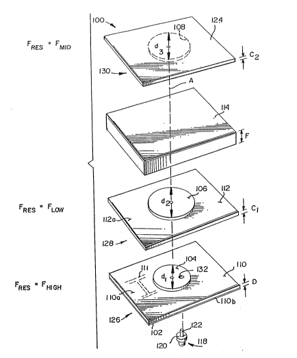
Figure 4 is a side view in cross-section of the
presently preferred exemplary embodiment of a stacked
microstrip antenna structure 100 of the pre ent invention.
Antenna structure 100 includes a conductive reference surface
~"ground plane") 102, a driven element 104, a first parasitic
element 106,
rn/
: .
. .
.. . . ...
` ( ~LZ~37~7
14
and a second parasitic element 108. Antenna
structure 100 may be termed a "three-resonator
parasitically coupled microstrip antenna array
element" because it includes resonant driven eleme~t
104 which is closely parasitically coupled to
resonant passive elements 106 and 108.
In the preferred embodiment, ground plane
102 and elements 104, 106, 108 are.stacked, and are
separated from adjacent elements by layers of
dielectric material. A dielectric layer 110 having
a thickness D separates ground plane 102 from driven
element 104; a dielectric layer 112 having a
thickness Cl separates driven eIement 104 and first
passive element 106; and a dielectric (typically
foam) layer 114 having thickness F separates passive
elements 106 and 108. Elements 104, 106 and 108.are
each circular (discoid) in shape in the preerred
embodiment (although rectangular, annular,
polygonal, etc. elements could be used instead if
desired).
~ .
In the preferred embodiment, driven
element 104 is connected to a transmission line (not
shown) via a conventional coaxial-type connector 118
(and via a microstrip if desired). Coaxial
connector outer conductor 120 is electrically
connected to ground plane 102, and the connector
center conductor 122 passes through~a~hole drilled
through ground plane 102 and dielectric layer 110
(without contacting the ground plane) and is~
electrically connected to driven element 104.
,.
. :
(
A further layer 124 of insulative material
(e.g., laminate) having a thickness C2 i~ di~posed
on and above passive element 108 to function as a
radome -- sealing antenna structure 100 from the
environment and helping to prevent damage to the
antenna structure.
FIGURE S is an exploded view in
perspective of antenna structure 100. Eabrication
of antenna structure 100 is particularly simple in
the preferred embodiment because conventional
printed circuit board fabrication technique~ are
used. Antenna structure 100 in the preferred
embodiment is fabricated by assembling ~ive
components; coaxial connector 118; a lowermost
printed circuit board structure 126 (of which ground
plane 102, dielectric layer 110 and driven element
lOg are integral parts); a midd].e printed circuit
board structure 12R (of which dielectric layer 112
and passive element 106 are integral parts);
dielectric layer 114 (which in the preferred
embodiment is a relatively thick layer of low loss
foam); and an uppermost printed circuit board
structure 130 (of which passive element 108 and
radome layer 124 are integral parts).
Printed circuit board fabrication
techni~ues are especially suited for microstrip
antenna element fabrication because of their low
cost and also because the dimensions of printed
circuit board laminates as well as the size of
conductive structures fabricated using such
~2~7:~
16
techniques are compatible with microstrip antenna
structure design.
For example, in the preferred embodiment,
lowermost structure 126 is fabricated from
conventional doubly-clad low loss PC board stock
(i~e., a sheet of laminate 110 having a sheet of
copper or other conductive material adhered to its
top surace llOA and another conductive material
sheet adhered to its bottom surface llOB) by simply
etching away (using conventional photochemical
etching techniques for example) all of the copper
sheet disposed on upper surface llOA except for that
portion which is to form driven element 104 while
leaving the cladding on bottom surface llOb
unetched. Additional RF circuits (e.g., a power
dividing network for array applications) may be
etched on surface llOa using the same process.
Similarly, printed circuit board
structures 128 and 130 are formed from low loss
single-clad printed circuit board stock by etching
away all of the single sheet of copper adhered
thereto except for t~lat portion which is to remain
as passive elements 106, 108, respectively.
To assemble antenna structure 100, the
coaxial connector center pin 122 is first pushed
through a hole 132 (drilled through discoid driven
element 10~) which has been found beforehand (e.g.,
through measurement) to provide a sui~able impedance
match for the transmission line to be connected to
connector 118. Pin 122 is conductively bonded to
`~ ( (
12~379~7
17
driven element 104 ~e.g., by a solder joint or the
like). Preferably, two microstrip transformer~
etched on surface llOa are also connected to pin 122
and used to rotate the antenna structure impedance
locus to a nominal 50 match. The coaxial connector
outer conductor is electrically bonded to ground
plane 102.
Next, PC board structure 128 is placed
onto upper surface llOa of PC board structure 126
with the center of discoid passive element 106 being
aligned with the center of driven element 104.
Then, foam layer 114 (which may be conventional
low-loss honeycomb-type material molded to specified 1p l/S/~
dimensions, Rhoacell-type foam machined to desired ~ y~k7
dimensions, or any other dielectric such as air, PTF~
or the like) is disposed on an upper surface 112a of
t PG board structure 128. Finally, PC board structure
130 is disposed on foam layer 114, with discoid
passive element 108 facing the foam layer and with
the center of that passive element being aligned
with the centers of elements 104 and 106 (so that a
common axis A passes through the centers of elements
lO~, 106 and 108). The entire structure so
assembled may be held together by applying
conventional film adhesive ~which can be used to
coat each layer prior to assembly), and then placing
the assembled structure in an autoclave.
As shown in FIGURES 4 and 5, elements 104,
106 and 108 have different dimensions. In the
preferred embodiment, the diameter d1 o element
104 lS less than the diameter d2 of element 106,
lZ87~7
18
which in turn i6 le~s than the dlameter d3 of
element 108. Elements 104, 106 and 108 each have
different resonant frequencies because of these
differences in dimensions.
Driven element 104, being smaller than
elements 106 and 108, has a resonant frequency of
fHIGH (a freq~lency at or near the high end of the
operating freguency range of antenna structure
100). Passive element 106 has a resonant frequency
f fLOW (a frequency at or near the low end of the
operating frequency range of antenna structure
100). Element 108 resonate at an intermediate
Y MID which is between fHIGH and f
Antenna structure 100 exhibits broadband
performance because the quality factors (Qs) and
dimensions of elements 104, 106 and 108 are chosen
to provide a degree of overlap between resonant
fre~uency ranges. That is, the sizes and spacings
of driven element 104 and passive element 108 are
chosen such that both of these elements resonate at
some frequencies between fHIGH and fMID ~~ and
similarly, spacings and dimensions of elements 108
and 106 are selected so that both of these el~ments
resonate for some frequencies between fMID and
fLOW'
Briefly, the bandwidth and operating
frequency range o~ antenna structure 100 is designed
by appropriately selecting the Qs and dimensions of
elements 104, and 106 and 108. The interactian
between elements 104-108 is complex and the analysis
- ~287~l7
19
used to select the spacings between the elements,
the dimensions of the elements, and the dielectric
constants of the intervening dielectric layera is
therefore non-trivial. A detailed theoretical
discussion about how these design choices are made
is presented below.
It is possible to describe in simple terms
the operation of antenna structure 100 as follows.
Excitation of driven element 104 by an RF signal
applied to the driven element via coaxial connector
118 may cause passive element 106 and/or passive
element 108 to be parasitically excited (if they are
resonant at the driving frequency) due to the
electromagnetic fields emanating from the driven
element. In a similar fashion, signals received by
elements 106 and/or 108 may cause those passive
elements (if they are resonant) to emanate
electromagnetic fields which parasitically excite
driven element 104.
The Qs of elements 104, 106 and 108 and
the frequency ranges at which each of these elements
resonate are selected so that, for any arbitrary
frequency within the design operating frequency
range of antenna structure 100, at least one and
possibly two of the t}lree elements is resonant. At
some frequencies at tlle low end of the operating
range, only element 106 is resonant. Similarly, at
some frequencies in the middle of the operating
range, only parasitic element 108 is resonant, and
at some frequencies at the upper end of the
operating range, only driven element 104 reaonates.
~2879~7
~The parasitic element(s) which do not resonate at a
particular frequency serve as director elements to
increase antenna gain.
- At some frequencies between the lower end
of the operating range and the middle of the range,
elements 106 and 108 may both resonate. Similarly,
at some frequencies between the middle of the range
and the upper end of the range, elements 104 and 108
both resonate.
Antenna structure 100 as a whole exhibits
a relatively wide, virtually continuous band of
resonant freqùencies (see EIGURE 8) that is simply
not possible to achieve with one or even two
microstrip elements -- or with multiple elements not
having the specific spacings and dimensions of the
present invention.
It is helpful, in designing the spacings
and dimensions of the antenna structure shown in
FIGURE 4, to independently mathematically model
portions of the antenna structure. While the
interactions between elements 104, 106 and 108 are
not readily susceptible to mathematical analysis due
to their complexity, each element 104, 106 and 108
may first be modelled separately (with respect
ground plane 102~ in order to establish initial
design parameters. Then, the effects of the
interactions between the elements (obtained
experimentally, empirically, and/or through computer
simulations) may be used to modify the design
parameters resulting from the mathematical modelling
lX8~91~ (
21
~o obtain desired antenna bandwidth, efficiency and
frequency operating range characteristics.
The basic microstrip antenna is a resonant
structure which is, in essence, a resonant cavity.
FIGURE 6A is a side view in cross-section of a
simple microstrip antenna which includes a ground
plane lS0, a radiator patch 152 and a separating
dielectric layer 154. A transmission line is
connected between the ground plane 150 and radiator
patch lS2 (e.g., via a coaxial connector 156) to
couple an RF signal across the antenna elements.
Element 104 and ground plane 102 of
antenna structure 100 of the present invention may
be modelled as one microstrip antenna; element 106
and ground plane 102 may be modelled as a second
antenna; and element 108 and ground plane 102 may be
modelled as a third antenna.
The simple microstrip antenna shown in
FIGURE 6A can be modeled by the parallel RLC circuit
shown in FIGURE 6B composed of fixed, lump
elements. Although t~le parallel RLC circuit model
cannot be used to predict radiation characteristics,
it can be used to closely predict the input
impedance characteristics of the FIGURE 6A antenna
with respect to the frequency (and thus, the
impedance characteristics of eàch of elements 104,
106 and 108).
The parallel RLC circuit model has an
associated quality factor "Q" which permits
- ~Z87~L7
Z2
bandwidth and efficiency calculations to be
performed. There are three bandwidth and efficiency
determining quality factors for a ~quare microstrip
patch antenna: Radiation 105s (QR); dielectric
loss (QD); and conductor loss (QC) Assuming a
rectangular microstrip element aspect ratio of 1:1,
radiation loss QR is given by
Q _
r ~ 2h , (1)
dielectric loss QD is given by
Qd = ta1 c where tan c is the dielectric loss
tangent , ( 2 )
and conductor loss QC is given by
Q = h where c =
c c5 ~ ~o , (3 )
where c5 = skin depth
f = actual frequency
a = conduct i v i ty
For a circular microstrip element, QC
and QD are the same for both circular and square
microstrip patch antennas, and QR is only slightly
different.
28q9~7
23
Bandwidth is a function of overall quality
factor and also of design voltage standing wave
ratio (VSWR). That is, bandwidth is expressed in
terms of a percentage of a desired center operating
frequency over which the antenna structure exhibits
a VSWR of less than or equal to a design VSWR.
Bandwidth is dependent upon the following eguations:
.
BW = VSWR - 1 ~ f ( 4 )
QT~
where QT = 1Q + Q + Q I (5)
The composite circuit quality factor QT
is thus always less than the lowest individual Q,
and maximum theoretical bandwidth (infinite) will
occur when any one Q approaches zero. However, if
either QD or QC approaches zero, all of the
available energy is absorbed and converted to heat,
leaving nothing to radiate. The following equations
show mathematically the interaction between the
individual quality factors and the overall
microstrip element radiation effici.ency:
power radia~ed = ~ where QL ~ Qloss IQd Qc
QdQc
Qd Qc
,
~~ 12~7~7
24
n = Q ~Qd ~ Qc) (7)
QdQc
Ideally, QD and QC should be high and
QR should be low -- this combination maximizes the
antenna impedance bandwidth and still maintains hlgh
radiation efficiency.
The individual Q parameters of the FIGURE
6A antenna can be controlled by the proper selection
of dielectric substrate, substrate thickness,
dielectric constant, conductor metallization,
conductance, and dielectric loss tangent. After
physical and material selections are made, the
individual quality factors are calculated and a
composite QT is then determined.
The calculated composite quality factor
QT of the microstrip element is calculated as a
"black box" value -- since values of the guality
factors associated with the distributed inductance,
capacitance and resistance of the antenna structure
are very difficult to measure i~ndividually. Thus,
when comparing the quality factor of a parallel RLC
lump network to the composite Q of a microstrip
element, the value of the indlvidual quality factors
of the microstrip element are no longer required,
and the microstrip eIement QT replaces the
paralleI RLC QS in t~e 'lumped element model.
- ~ ~2~
In order to complete the RLC modelling of
the FIGURE 6A antenna structure, a value of R at
resonance (frequency = Fo) of the microstrip
antenna may be calculated -- or e~perimentally
determined using network analysis of locus Sll on
a Smith Chart plot of the measured antenna impedance
characteristics. The RLC model is more accurate if
the resistance R of the microstrip antenna at
resonance is actually measured, since the microstrip
element composite quality factor QT is calculated
rather than measured. This R value may be obtained
by plotting the measured impedance of the microstrip
antenna on a Smith chart and noting the real
impedance where the Sll locus crosses the real
axis o~ the Smith Chart (this is also where the
resonant frequency of the microstrip antenna occurs).
By using the following circuit analysis
equations, it is possible to complete the parallel
RLC model derivation:
(8)
Q = QT = calculated
F = fO = measured (wO = 2~fo) (9)
R = Rf = measured
o
(10)
and finally,
C = w-Q and L = R (11)
(
1~37!3~7
26
This model is quite accurate, and greatly simplifies
-the design and analysis of antenna structure shown
in FIGURE 4.
The following procedure may be followed to
select the various design parameters for antenna
structure lOO of the present invention.
First, the overall element design
bandwidth, maximum VSWR, and radiation efficiency
are specified. These parameters are generally
design constraints associated with a particular
application. For example, the efficiency and
maximum VSWR of antenna structure lOO may be
selected to accommodate a particular radio
transceiver power output stage and/or a desired
communications range or effective radiated power
(ERP). Overall element bandwidth is specified
according to the range of frequencies over which
antenna structure lOO is to operate (for example,
some common operating frequency ranges are the L
band, 1.7 - 2.1 GHz; the S-band, 3.5 - ~.2 GHz; and
the C-band, 5.3 - 6~5 GHz).
Next, proposed substrate thicknesses,
dielectric constants, metallization thicknesses and
loss tangents are c~osen based on desired mechanical
strength and desired efficiency (some of these
factors may also be determined by the properties of
available materials).
Then, the RLC mathematical modelling
discussed above is used to calculate the QR' QD
~2 8 7 917
27
and QC of each of elements 104, 106 and 108
individually, and QT is calculated for each
element (using the assumption that there i8 no
interaction between the elements).
The QR' QD and QC for each of
elements 104, 106, 108 is calculated by evaluating
equations 1-3 for the proposed substrate thickness,
dielectric constant, metallization thickness and
loss tangent. Then, the composite quality factor
QT for each of elements 104, 106 and 108 is
calculated according to equation 5.
Finally, the.individual resonant
frequencies are determined (by measurement,
calculation, empirical analysis and/or computer
simulation) to determine the overall bandwidth and
maximum VSWR of antenna structure 100.
After performing these last two steps, it
may be necessary to change the substrate parameters
and iteratively recalculate antenna performance
characteristics until the design specifications are
satisfied. The efficiency as well as the composite
QT of each individual element is unique -- and
therefore, the resonant frequency separations are
not linear about the "center frequency" of the
overall antenna structure 100. Likewise, the
efficiency of structure 100 may vary slightly with
frequency, depending upon which of elements 104, 106
and 108 is acting as the primary radiator (in
addition, the other elements may or may not,
~l2879~7
28
depending on frequency, act as directors to improve
antenna gain).
Inter-element capacitances and their
effects on resonant frequencies and radiation
characteristics are not mentioned in the previous
discussion. ~owever, these parasitic capacitances
(without which antenna structure 100 will not work
as desired) are non-trivial -- and more importantly,
they are very difficult to model analytically.
Nevertheless, it is possible to schematically
describe elements 104, 106 and 108 along with their
inter-element capacitances, and than determine the
parasitic values empirically using computer curve
fitting routines.
FIGURE 9 is a schematic diagram of the
lump-element equivalent circuit model of antenna
structure 100. Each of elements 104, 106 and 108
ma~ be modelled as a parallel RLC circuit (as
described in connection with FIGURES 6A and 6B).
Capacitances 166, 168 and.170 are the capacitances
from elements 106, 108 and 110, raspectively, to
ground plane 102. Three parasitic capacitances are
also included in the model shown in FIGURE 9: A
capacitor 160 (the parasitic capacitance between
elements 104 and 106); a capacitor 162 (the
parasitic capacitance between elements 106 and 108);
and a capacitor 164 (the parasitic capacitance
between elements 104 and 108). FIGURE 10 is a
schematic side view of antenna structure 100 also
showing these parasitic capacitances.
~87~1~
29
The middle passive element 106 resonates
and operates at frequencies at the lower end of the
operating frequency range of antenna structure 100
in the preferred embodiment. When element 106 is
physically covered by element 108, the resonant
frequency of element 106 drops approximately 8-9%
(this change in resonant frequency is also due, in
part, to inter-element capacitances). The
inter-element parasitic capacitances present when
antenna structure 100 is operated at some frequency
FLoW at the low end of its range are schematically
shown in FIGURE 11.
Passive element 106 is excited at FLoW
by driver element 104 through parasitic capacitance
160. Actual radiation occurs because of capacitance
166 (from element 106 to ground plane 102).
Capacitance 166 is also modelled schematically in
FIGURE 9 as a parallel RLC circuit. Parasitic
capacitor 162 (a series capacitance between passive
elements 106 and 108) causes passive element 108 to
act as a radiation director, causing a slight
increase in gain).
FIGURE 12 is a schematic diagram of
antenna structure 100 showiny the inter-element
parasitic capacitances present when the antenna
structure is operated at some frequency FMID which
is approximately in tlle middle of its operating
frequency range. At such middle frequencies,
uppermost parasitic element 108 is responsible for
most of the radiation emitted from antenna structure
100 in the preferred embodiment. The resonant
~Z~7~
frequency of uppermost pas~ive element 108 i8
lowered by approximately 2-3% from its predicted
value because it is covered by dielectric radome
layer 124.
Element 108 is excited by driven element
104 through parasitic capacitance 164 (between
elements 104 and 108). Actual radiation occurs
because of the capacitance 168 between element 108
and ground plane 102. Capacitance 168 is also
modelled schematically in FIGURE 9 as a parallel RLC
structure. The midband gain of antenna structure
100 is reduced slightly since there are no elements
above element 108 to act as directors.
FIGURE 13 is a schematic illustration of
antenna structure 100 showing the parasitic
inter-element capacitances present when the antenna
structure is operated at some frequency FHIGH at
the high end of its frequency operating range.
Driven element 104 resonates at FHIGH and, because
it has elements 104 and 108 directly above it acting
as directors, the antenna structure exhibits an
overall effective increase in gain. The resonant
frequency of driven element 104 is about 8-9% lower
than it would be if elements 106 and 108 were not
present (inter-element capacitances play a role in
this resonant frequency shift). The capacitance 170
between driven element 104 and ground plane 102 is
modelled schematically in FIGURE 9 by a parallel RLC
circuit.
` ~7917
The following TABLE I lists exemplary
design specifications for three different
embodiments on antenna structure 100: An L Band
configuration; an S-Band configuration; and a C-Band
configuration.
TABLE I
L Band S-Band C-Band
(1.7-2.1 (3-5-4.2 (5.3-6.5
GHz~ GHz) GHz)
D 0.060 0.031 0.020
dl 1.855 0.951 0.644
Cl 0.015 0.005 0.005
d2 2.359 1.209 0.7845
F 0.375 0.165 0.113
C2 0.015 0.015 0.015
d3 2.690 1.336 0.840
E 2.44 2.17 2.17
r
BW 17% 17% 19%
VSWR1.5:1 1.5:1 1.4:1
where D = thickness o~ dielectric layer 110 in
inches, dl = diametcl- of element 104 in inches,
Cl = thickness of layer 1;12 in inches, d2 =
diameter of element 106 in inches, F = thickness of
foam layer 114 (71/WF Rhoacell), C2 = thickness of
layer 124 in inches, d3 = diameter of element 108
in inches, Er = the dielectric constants of layers
110, 112 and 124 (which have the same dielectric
~L~379~ !
constants in the preferred embodiment), and ~W = the
actual measured bandwidth of the antenna structure
for the VSWR stated.
As can be seen from TABLE I, there i5 an
indirect relationship between the dimensions and
spacing parameters of antenna structure 100 and
operating frequency. That is, if the operating
frequency is doubled, all spacings and dimensions
are cut approximately in half. Thus, approximate
parameters for antenna structure 100 for any given
operating fre~uency can be derived from the
parameters set forth in TABLE I for an antenna of a
different operating ~requency.
Thus, if C1 = x, then D = 4x for any given
frequency. Similarly, if d3 = y, then d2 =
.9Oy, and d1 =.70y. The dimension D can be varied
depending upon desired overall bandwidth (since the
bandwidth of the antenna structure is directly
dependent on the dimension of D). Thus, D can be
increased to greater than 4x if still broader
bandwidth is desired and decreased to less than 4x
if the antenna does not need to operate over a very
wide range of frequencies. However, C1 should be
approximately the value described previously for a
given operating frequency. The values d1, d2
and d3 are dependent upon the dielectric constants
of the composite substrate used, and therefore may
have to be adjusted if material5 ~ifferent than
those described herein are used.
2l~79~L7
FIGURE 14 is a graphical illustration o
the gain versus frequency response curve of antenna
structure 100. As can be seen, the gain of antenna
structure 100 is not constant with fre~uency, but
instead varies due to the director effects of
elements 106 and 108 at certain frequencies (as
previously discussed).
FIGURES 7 and 8 graphically show the
overlapping resonances of elements 104, 106 and
108. FIGURE 7 is a plot of the bandwidths of
elements 104, 106 and 108 taken individually --
that is, as calculated independently for each
element using the RLC modelling discussed above and
assuming there is no interaction between the
elements.
FIGURE 8 is a plot of the actual frequency
vs. VSWR plot of antenna structure 100. Although,
as shown in FIG~RE 7, each element 104, 106 and 108
has relatively sharp resonance curve (determined by
the QTS of the individual elèments), these sharp
curves "blur together" in the bandwidth plot of the
composite antenna structure shown in FIGURE 8 due to
the interaction between the elements.
Thus, the overall bandwidth of antenna
structure 100 for a particular VSWR (e.g., 2.0:1) is
substantially greater than the bandwidth which could
be obtained by simply connecting without closely
coupling the three elements together as in the
present invention.
~2~3~9
34
- Antenna structure 100 e~periences varying
degrees of polarization degradation with operating
frequenc~. The amount of degradation depends upon
which of elements 104, 106 and 108 is operational.
When element 108 is active, the cross-polarized
radiation level is at its lowest value for antenna
structure 100. However, the cross-polarized
radiation level is worse when element 106 is active,
and is still worse when element 104 resonates. Even
still, antenna structure 100 exhibits isolation
between co-polarized and cross-polarized components
of approximately -16dB or better at the highest
frequencies within its operating range (i.e., when
driven element 104 is resonant~.
The change in cross-polarized radiation
levels with frequency is easily explained by looking
at the physical structure of antenna structure lO0
shown in FIGURE 4. Driven element 10~ has two
elements above it, and passive element 106 has one
element above it. These upper elements cause
changes in polarization purity -- more for driven
element 104 (because there are two elements above
it) than for element 106 (which has only one element
above it). In other words, energy radiated from the
lowermost element is disturbed by the close
proximity of non-resonant elements in the direction
of propagation.
Antenna structure 100 as described forms
an "inverted stack" (that is, the element ha~ing the
smallest dimension is lowermost in the stack). This
inverted stack structure has the advantage that very
~2~379~7
little "real estate" on dielectric layer surface
llOa (of PC board structure 126) is occupied by
lowermost element 104, leaving room for additional
RF circuitry (for example, a power dividing network)
to be etched on laminate surface llOa. It i8
inexpensive and relatively simple to fabricate
whatever additional RF circuitry is desired on
laminate surface llOa, thus providing additional
features in the same size antenna package and
obviating the need for externally-provided RE
circuitry.
Further advantages are obtained from the
feature that the lowermost element 104 is directly
connected to a transmission line and serves as the
driven element (thereby obviating the need for
feed-throughs and the like). If no additional RF
circuitry is to be provided on lowermost PC board
structure 126, it may be desirable in some instances
to make the dimensions of driven element 10~ larger
than the dimensions of one or both of elements ].06
and lOa. For example, it might be desirable to
select the dimensions of driven element lO~ so that
the driven element resonates at the middle of the
frequency operating range of the antenna structure,
and to make element 106 larger than elements 104 and
108 (so that middle eIemellt 106 resonates at lower
end of the fre~uenc~ range and uppermost element 108
resonates at the upper end of t~e frequency range).
This configuration has been experimentally verified
to have a 1.8 VSWR bandwidth of about 23~. However,
in order to optimize antenna structure lO0 to enable
etching of an arra~ power di~ider on the same
-
- ( ~287~7
36
substrate as that supporting driven element 104, the
resonant frequency of the driven element was changed
from midband to F~IGH in the preferred embodiment-
While the present invention has beendescribed with what is presently considered to be
the most practical and preferred embodiments, it is
to be understood that the appended claims are not be
limited to the disclosed embodiments but on the
contrary, are intended to cover all modifications,
variations and e~uivalent arrangements which retain
any of the novel features and advantages of this
invention.
.~