Note: Descriptions are shown in the official language in which they were submitted.
~.2~
ANALO~-TO^DI~ITAL ~ONVERTER
WITH ADAPTABLE QUANTIZING LEVELS
Technical Field
The present invention relates to an analog-to-digital converter
and, more particularly, to an analog-to-digital (A/D) converter whose
quantizing levels are adjusted in response to variations in the range of the
5 analog signal amplitude.
Background of the Invention
A/D converters are a basic building block for the system
designer and a myriad of different designs are available. In certain system
applications, the analog input signal is subject to unpredictable and
10 significant attenuation. In other applications, the incoming analog signal at a hub location arrives from a number of remote locations via different
communication paths. The signal amplitude in these paths experience
unwanted amplitude fluctuations which vary in time and from one path to
another. Such signal effects can decrease the sensitivity provided by an
~5 A/D converter used in these system applications and, in turn, result in
substantially degraded system performance. One way of compensating for
such effects is to interconnect an automatic gain control device in the
analog input signal path to maintain a predetermined signal amplitude.
While this arrangement provides satisfactory results, the resulting circuitry
20 can be complex and not amenable to meet the size and cost objectives of
certain system applications. Accordingly, an A/D converter which
maintains a prescribed sensitivity during the presence of analog signal
amplitude fluctuations and which can be provided with digital devices at
low cost would be desirable.
25 Summary of the Invention
In its broadest aspect, the present invention overcomes the
shortcomings of the prior art by adjusting the distance between the
quantizing levels of an A/D converter in response to an examination of the
converter's digital output signals. This arrangement advantageously
30 maintains the amplitude swing of the analog A/D converter input signal
within the distance between the outermost quantizing levels so as to
maintain a constant converter sensitivity. In the disclosed embodiment,
selected bits of the A/D digital output are examined by circuitry which
- , :
72~
expands or compresses the distance between the outermost
quantizing levels from which the other quantizing levels are
derived.
An aspect of the present invention is that it can be
readily adapted to system applications wherein the analog
- input signal arrives in bursts or packets. In such system
applications, the quantizing levels are maintained at the
existing states during the absence of an analog input signal.
Another aspect of the present invention is that is can be
.lO arranged to store the adjusted quantizing levels for analog
signals arriving from each of a plurality of different
communications paths. The adjusted quantizing levels
associated with a given path are then used in the A~D
converter each time the analog signal arrives over the given
path.
In accordance with one àspect of the invention there
is provided signal conversion apparatus comprising an analog-
to-digital converter having a plurality of quantizing levels
extending over a predetermined range, said converter assigning
the amplitude of an analog data signal at each of a plurality
of predetermined times to one of said plurality of quantizing
levels, the assignment providing a digital output comprising a
plurality of bits whose values are independent of one another,
and means responsive to said digital output for varying said
predetermined amplitude range, said varying means expanding
said predetermined range in response to one value of a
predetermined bit in each digital output and compressing said
predetermined range in response to another value of said
predetermined bit.
In accordance with another aspect of the invention
there is provided a method of adjusting an analog-to-digital
converter, said method comprising the steps of assigning an
analog data signal amplitude at each of a plurality of
predetermined times to one of a plurality of quantizing levels
which extend over a preselected range, the assignment
providing a digital output comprising a plurality of bits
whose values are independent of one another, and varying said
f'~
. ~, ,. ~
' ' ' ' ': ,'
:, '' - ' ~ ' , '
, ~ .
~l2875';~
2 a
preselected range in response to said digital output said
varying means expanding said predetermined range in response
to one value of a predetermined bit in each digital output and
compressing said predetermined range in response to another
value of said predetermined bit.
Brief Description of the Drawina
FIG. 1 is a block schematic diagram of an embodiment
of the present invention;
FIG. 2 is a block diagram of an illustrative system
to which disclosed embodiment pertains; and
FIG. 3 is a diagram which is useful for
understanding the operation of the disclosed embodiment.
Detailed Descri~tion
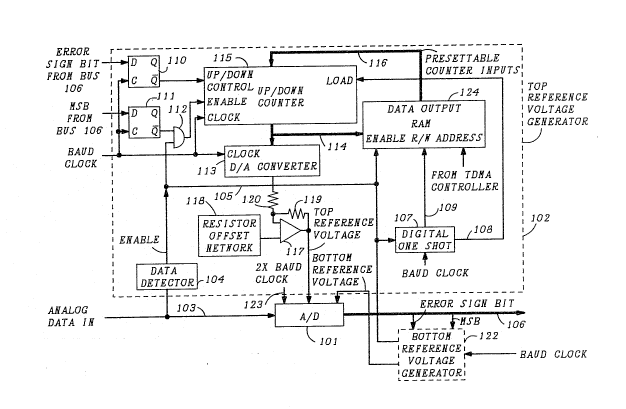
Referring to FIG. 1, an analog data signal on lead
103 is coupled to A/D converter 101 and data detector 104.
This analog signal conveys information on a plurality of
discrete amplitude levels at a predetermined baud or symbol
rate. While these information-carrying amplitude levels are
generally fixed at the transmitter, distortion over the
transmission channels causes the information-carrying signal
levels in the received analog data signal to vary.
A/D converter 101 quantizes the analog signal
amplitude on each occurrence of a clock signal to the
closest one of a number of quantizing levels. This clock
~5 signal, at twice (2X) the baud rate, is coupled to A/D
converter 101 via lead 123. The number of quantizing
levels utilized by converter 101 is variable and depends
on the system application. In general, there can be two
or more such levels. Each output of A/D converter 101
3~ appears on bus 106 in the form of a digital word having a Ir
predetermined number of bits. Predetermined ones of
these bits are coupled to top reference voltage generator
102 and bottom reference voltage generator 122
5 ~
.
. : .
1~3792~L
which, as will be described, adjust a pair of reference voltage levels in
response to variations in the analog signal amplitude so that this
adjustment assures that the voltage swing of the incoming analog data
signal always lies within the distance between the outermost quantizing
5 levels. As a result, the sensitivity or accuracy of the A/D converter output
is maintained despite undesired attenuation or amplification of the
incoming analog data sign.al.
Refer now to FIS~I. 2 which shows an illustrative radio system
using time division multiple access (TDMA) to which the present invention
10 pertains. As shown, system 200 provides two-way radio communications
between a hub location 201 and a plurality of remote locations 202-1,202-
2~..202-N. An A/D converter, in accordance with the present invention, is
disposed at the hub and at each remote. Data arrives at the hub and
remote locations in bursts, with the exception tha~ if the hub is loaded to
15 capacity, its A/D converter is supplied with a continuous analog input
signal.
The communications channels 203-1 through ~03-N between
each remote location and the hub are different and subject at any given
time to different degrees of fading and other forms of distortion. ~or
20 example, in an actual system, the incoming signal at the hub location may
contain short-term power level variations of +/- 2 dB, while the incoming
signal at a remote location may contain long-term power level variations of
several dB. Short-term variations are those that occur from one data burst
to the next and occur at the hub location, for example, when remote
25 locations with different power levels transmit information to the hub
location in adjacent bursts. Long-term power level variations occur more
gradually and can have periods of days, yearsj or the system lifetime and
occur at either a hub or remote locat;on, for example, when the radio
system's automatic gain control does not fully compensate for a change in
30 the transmitted signal power caused by distortion over the channel, such as
fading. In any event, such unwanted variations reduce the sensikivity
provided by many A/D converters if the total possible number of levels to
which the analog signal can be quantized varies. The present invention can
be adapted for use in the illustrated hub or remote locations and can be
35 used in systems wherein the transmission is not continuous to preclude any
,'. ,.": .
' ' ' "' .' ' ~ .
79;~ ~l
degradation in the sensitivity provided by an A/D converter in the presence
of unintended variations in the power level or amplitude OI the analog data
signal.
To best understand the operation of the disclosed embodiment,
5 refer now to FIG. 3. For purposes of illustration, it shall be assumed that
A/D converter 101 utilizes 256 uniformly separated quantizing levels and
that the incoming analog data signal on lead 103 is in the form of an
amplitude modulated pulse sequence derived from one carrier of a pair of
quadrature-related carrier signals. Each of such carriers were modulated at
10 a transmitter using a 16 QAM format. It is understood, of course, that the
present invention is not limited to such a modulation format but can be
used with any format from which a pulse amplitude modulated sequence
can be derived.
FIG. 3 shows an idealized signal-eye diagram 301 for a 16 QAM
15 modulation format and nine of the quantizing levels used by A/D
converter 101. These nine quantizing levels are designated as 302-310. Two
of these nine levels, namely, outermost levels 302 and 310, are also the top
and bottom reference voltage levels. Levels 302, 30~, 306, 308 and 310
define the boundaries of four sub-regions, 320-323, and the midpoint of each
20 of these sub-regions respectively coincides with levels 303, 305, 307 and 309.
The remaining 247 quantizing levels (not shown) are evenly dispersed across
the four sub-regions. ~ach of these nine quantizing levels along with each
OI the other 247 quantizing levels is represented by an 8 bit word. FI(~. 3
also shows the 8 bit words corresponding to each of the illustrated
25 quantizing levels. In a 16 QAM format, each modulated carrier signal
conve~vs information on any of four amplitude levels and these four
amplitude levels have the values of -3, -1, +1, and -~3 volts and respectively
correspond to levels 303, 305, 307 and 30~.
The arrangement of bits in each 8 bit word is determined using
30 two's complement mathematics. For 16 QAM modulation, 2 bits of each 8
bit word represent one of the four possible transmitted amplitude levels and
the remaining 6 bits denote the error or difference between the analog signal
quantized by converter 101 and the closest one of the four possible
transmitted signal levels. Specifically, the most-significant bit (MSB) or
3~ leftmost bit and the next most-significant (NMSB) bit in each output word
28';792~5L
-- 5 -
denotes the closest one of the four possible transmitted signal levels to the
analog data signal on lead 103 at each quantizing time. Referring to FIG. 3,
the MSB and NMSB of the quantizing levels Iying in sub-region 320 are
logical "1" and "0", respectively, and denote a transmitted signal level of
5 -3 volts. Similarly, the quantizing levels in sub-regions 321-323, respectively,
have an MSB and NMSB of logical "1" and "1", logical "0" and "0", and
logical "0" and "1" to denote transmitted signal levels of -1, +1 and
+3 volts. In addition, the MSB of all of the 8 bit words denotes the polarity
of the quantized analog signal. Accordingly, an MSB of logical "0" indicates
~0 a positive polarity and is such for all quantizing levels in sub-regions 322
nnd 323, and an MSB of logical "1" indicates a negative polarity and is such
for all quantizing levels in sub-regions 320 and 321. This polarity indication,
as will be described, is advantageously utilized in the disclosed embodiment
to provide independent adjustment of the top and bottom reference levels.
As previously stated, 6 bits in each 8 bit output word indicate
the error of the quantized analog signal at each quantizing time with respect
to the closest one of the four possible transmitted signal levels. In addition,
one of these 6 bits indicates the polarity or sign of this error. This error
sign bit (ESB)is the third bit position from the left in each 8 bit output
20 word and is shown in FIG. 3. As illustrated, any quantizing level Iying
below the middle of its associated sub-region has a logical "0" ESB and any
quantizing level Iying above the middle of its associated sub-region has a
logical "1" ESB. For example, quantizing levels for sub-region 322 Iying
between levels 306 and 307 have a logical "0" ESB and those quantizing
25 levels Iying between levels 30~ and 308 have a logical "1" ESB. The ESB,as
will be describsd hereinafter, is used by the present invention to optimally
position the quantizing levels. In this regard, it should be noted that if the
distortion producing the error in the quantized analog signal is random,
then there is an equal likelihood of the ESB being a logical "0" or "1".
30 However, if the analog signal is attenuated by distortion, then there is a
greater occurrence of logical "Os" than logical "1s" for analog signals Iying insub-regions 322 or 323. Similarly, if the signal at one time is amplified, then
there is a greater occurrence of logical "1s" than logical "Os" for analog
signals Iying in sub-regions 322 or 323. The opposite result applies for
3S signals Iy;ng in sub-regions 320 and 321. The present invention corrects
,
'
2~3~9
- 6 -
both of these situations, which can result in an incorrect determination of
the transmitted signal levels, by integrating the ESB on bus 106 and varying
the position of the quantizing levels in response thereto.
Now, refer back to FIG. 1. Data detector 104 in top reference
5 voltage generator 102 ascertains the presence of the analog data signal on
lead 103 and provides an enable signal which is coupled to one input of
AND gate 112, digital one shot 107 and to RA:M :124. Detector 104 is
advantageously utilized when the disclosed embodiment is disposed in a
location, such as the hub or any of the remote locations 202-1 through 202-
10 N of FIG. 2, wherein the analog signal may be received in bursts. RAM 124is preferably employed when the disclosed embodiment is used in a location
where the incoming analog data signal is received from different
communication paths, such as in the case of signals arriving at hub
location 201 of FIG. 2.
D-type flip-flops 110 and 111, strobed by the baud clock,
respectively toggle the MSB and ESB to their Q outputs on each occurrence
of the baud clock. The Q output of flip-flop 111 is coupled to an input of
AND gate 112 which produces a logical "1" pulse when an analog data signal
is present on lead 103 which falls into either sub-region 322 or 323 of FI~. 2.
20 This losical "1" output enables up/down counter 115. Accordingly, this
counter only responds for analog data signals having a positive polarity.
Once enabled, up/down counter 115 increments its count by one for each
logical "1" Q output of flip-flop 110 and decrements its count by one for
each logical "0" output of this flip-flop. Ii~ not enabled, counter 115
25 maintains its stored count or accepts a new count via bus 116. Accordingly,
if the top reference voltage is optimally positioned, the count stored by
counter 115 oscillates about some fixed count in response to positive
polarity analog data signals. Such optimal positioning occurs when there is
an equal likelihood of a positive or negative error signal polarity for a
30 quantized positive polarity analog signal. If, however, the value of the top
reference voltage is too low or, equivalently, the positioning of outermost
quantizing level 310 is too low, the count stored in counter 115 will increase
and, in response thereto, top reference voltage generator 102 will increase
the top reference voltage so as to raise the position of outermost quantizing
35 level 310 to the optimal position. Similarly, if the top reference voltage or
1~7~2~L
-- 7 --
the position of quantizing level 310 is too high, the count stored in
counter 115 will decrease and the top reference voltage and position of
outermost quantizing level 310 will be lowered by generator 102.
T~e count stored in counter 115 appears on bus 114 and is
5 coupled to D/A converter 113 wherein it is transformed into an analog
signal on each baud clock pulse. This analog signal is coupled to one input
of difference amplifier 117 which is configured with input and feedback
resistors 120 and 119, respectively. Resistor offset network 118 supplies an
offsetting signal to the other input of difference amplifier 117. The output
10 of difference amplifier 117 is the top reference voltage which is supplied to A/D converter 101. This top reference voltage along with a bottom
reference voltage provided by bottom reference voltage generator 122
determines the positioning of the other 254 quantizing levels.
Advantageously, the positioning of the quantizing levels corresponding to
the maximum and minimum transmitted signal levels, i.e, quantizing
levels 303 and 309,is set to extend over 3/d~ of the distance between the top
~d bottom reference voltages via the offset signal provided by network 118.
In addition, to prevent false locks, the swing of D/A converter 113is
preferably limited to +/- 32 least significant bits around quantizing
20 levels 303 and 309.
When the disclosed embodiment is used in applications such as
hub location 201, storing the optimal position of the top reference voltage
for analog data signals arriving from each of a plurality of remote locations
advantageously reduces the convergence time of the adaptive circuitry. To
~5 achieve this benefit, R~AM 124 stores the count of counter 115 appearing on
bus 114. A read/write control pulse, which extends for one baud clock
period, is provided by digital one shot 107 for RAM 124 in response to the
enable signal on lead 105. The rising edge of this pulse serves as a read
signal for the RAM and the trailing edge serves as a write signal. This pulse
30 on lead 108 from digital one-shot 107 also serves as a load signal for
counter 115. Accordingly, at the onset of an analog data burst from a
particular remote location, the count of counter 115 associated with the last
transmitted data burst from this particular remote location is read out from
the RA:M and loaded into counter 115 via bus 116. Bus 116 is connected to
the presettable counter input terminals. At the end of the burst, the
~ ~7~Z~
-- 8 --
current state of counter 115 is written into RAM 12~ and is used as an
initial count for the next transmission from this particular remote location.
The RAM memory address into which and from which the coun-t is stored
and retrieved is controlled by the TDMA controller (not shown). This
5 controller, in well-known fashion, assigns the TDMA time slots in
accordance with a predetermined algorithm to the various remote locations.
Use of RAM 124 and digital one shot 107 is not required in applications
whereln the analog data signal is not arriving over different transmission
paths. In such case, these devices can be deleted and the presettable
10 counter input leads of counter 115 are grounded.
Bottom reference voltage generator 122 includes substantially
identical circuitry to that described for generator 102 to provide control of
the bottom reference voltage independently of any change in the top
reference voltage. This advantageously allows for unsymmetrical unwanted
15 amplitude shifts of the analog data signal on lead 103. The up/down
counter in generator 122 is only enabled when analog data is present which
lies in either sub-regions 320 or 321. If there are more logical "0" ESBs than
logical "1" ESBs, generator 122 lowers the bottom reference voltage or
position of quantizing level 302. Similarly, if there are more logical "1"
20 ESBs than logical "0" ESBs, generator 122 raises the bottom reference
voltage or position of quantizing level 302. A/D converter 101 utilizes a
resistor ladder, in well-known fashion, to derive the position at each of the
quantizing levels located between the outermost quantizing levels 302 and
3~0. Accordingly, a change in the position of either quantizing level 302 or
25 310 will produce a corresponding change in the location of each of the other
quantizing levels.
It should, of course, be understood that while the present
invention has been disclosed with respect to a particular embodiment,
numerous modifications should be apparent to those skilled in the art. l~or
30 example, while uniformly-spaced quantizing levels are used in the disclosed
embodiment, the spacing between successive quantizing levels need not be
the same but can vary in accordance with any formulation. Or, while both
of the outermost levels are adjusted in the disclosed embodiment, either one
of these levels can be flxed and the other level adjusted if such is desirable.