Note: Descriptions are shown in the official language in which they were submitted.
~.2~3~9;~4
83-445
-1 -
BACI~GROUND OF T~IE INVENTION
1. Field of the Invention
The invention relates generally to the field of digital
data processing systems.
~, Descri~tion of the Prior Art
A typical digital data processing system includes three
basic elements, namely a processor element, a memory
element, and an input/output element. The memory element
stores information in addressable storage locations. This
information includes both data and instructions for
processing the data. The processor element includes one or
more digital data processing units, or "processors", each of
which causes information to be transferred, or fetched, to
it from the memory element, interprets the incoming
information as either instructions or data, and processes
the data in accordance with the instructions. The results
are then stored in addressed~locations in the memory
element.
~b
. .
.. ; .. ...
.,. .. ,~.... .... .......
-; ` -. ~.. .~ ... ,;
~" .
~,2~37~Z~
B3~445
-2-
The input/output element also communicates with the
memory element in order to transfer information into the
system and to obtain the processed data from it. Vnits
comprising the input/output element normally operate in
accordance with control information supplied to it by the
processor element. The control information defines the
operation to be performed by the input/output unit. At
least one class of operations performed by an input/output
unit is the transfer of user information, that is,
information used by a user program, between the input/output
unit and the memory element. Typical units comprising the
input/output element include, for example, printers,
teletypewriters, and video display terminals, and may also
include secondary information storage devices such as disk
or tape storage units.
In addition to functioning as input/output devices,
disk storage units and, sometimes, tape storage units may
also function as part of the memory element. In particular,
a memory element typically includes a main memory, whose
contents are accessible to the processor relatively quickly
but which is generally relatively high-cost storage. Modern
main memories are typically implemented using MOS or bipolar
.. . . .. .
: ' :, ;' .',' ' ":' ::
~,,
" ,.
~2~3792A
83-445
--3--
semiconductor technology and may provide on the order of a
fraction of a megabyte to several tens of megabytes of
storage.
A major bottleneck in processing of data by a processor
is in the transfer of the instructions and data to be
processed to the processor and the transfer of the processed
data to other portions in the system. Transfers between the
processor and the memory element are typically of data and
instructions, and transfers between the processor and
input/output element are typically of control information
for controlling the operation of the input/output element,
although the processor may also transfer data with some
types of input/output units. A processor in a digital data
processing system includes an interface circuit for
transferring information with these units.
A processor also typically comprises several functional
portions, including a cache memory for storing immediately
used data and/or instructions, data path circuits for
performing primitive arithmetic and logic operations to
process the instructions, and control circuits for
interpreting the instructions, enabling the operands, or
data to be processed, to be obtained, enabling the data path
. . .
,
~2~ 4
83-445
--4--
to perform a series of operations to enable the operation
identified by an instruction to be performed, and enabling
the processed data to be stored. The transfer of
information among the various internal functional portions
of the processor is quite complicated, particularly when the
processor includes a cache memory and supports virtual
processing, and thus must provide virtual to physical
address translation.
SUMMARY OF T~E INVENTION
The invention provides a new processor for use in a
digital data processing system.
In brief summary, a processor for use in a digital data
processing system includes a bus interface circuit for
transferring data to and from other units in the system and
for controlling the transfer of information within the
processor over an internal bus. The bus interface circuit
includes two state machines, one for controlling the
internal transfers of information, and the other for
controlling the external transfers of information. The
state machines communicate through flags which indicate when
external operations are pending. A plurality of latches are
, .
~l2879~
60412-1-796
provided to receive write data, a write address and a read address
from other portions of the processor, and an inpu~ latch receives
signals from other units in the system, there~y allowing both a
write operation and a read operation to be initiated at the same
time. The processor continues operating unless another operation
is required.
The invention may be summarized, according to one
aspect, as a processor including a processing circuit for
processing information and a bus interface circuit for connection
to a bus for transferring information over said bus from other
units in a digital data processing system to said processing
circuit for processing and for transferring processed information
over said bus from said processing circuit to said other units,
said inter~ace circuit including: A. an input latch connected to
said processing circuit and for connection to said bus for
latching information received from another unit for transfer to
said processing circuit; B. an output latch connected to said
processiny circuit and for connection to said bus for latching
information from said processing circuit for transfer to another
unit; C. an interface control circuit including: i. an internal
state control circuit connected to said processing circuit, said
output latch and said input latch for controlling information
transfers between said processing circuit and said output latch
and said input latch; ii. an external state control circuit
connected to said input latch, sald output latch and for
connection to said bus for controlling information transfers
between said other units and said input latch and said ou~put
:
. .
'. .
.';'
~28~glZ4
60412-1796
latch; and iii. a condition indicator connected to said internal
state control circuit and said e~ternal state control circuit and
controlled by said internal state ~ontrol circuit to have a
selected condition in response to conditions of said input latch
and said output latch to thereby control operations of said
external state control circuit.
BRIEE DESCRIPTION OF T~E DRAWINGS
1'his invention is pointed out with particularity in the
appended claims. The above and further advantages of this
invention may be better understood by referring to the following
description taken in-conjunction with the accompanyiny drawings,
in which:
Fig. lA is a general block diagram of a digital data
processing system which incorporates the invention, and Fig. lB is
an organizational block diagram of a processor used in the system
depicted in Fig. lA;
Fig. 2, comprising Figs. 2A through 2D, is a timing
diagram useful in understanding the inventlon;
Fig. 3 is a detailed block diagram of a portion of the
~0 processor depicted in Fig. lB particularly relating to the
; . "
,
z~
83-445
--6--
circuits for controlling transfers with other portions of
the system.
DETAILED DESCRIPTION OF AN ILLUSTRATIVE 13MBODIMENT
General Description
Referring to Fig. 1, a data processing system including
the invention includes, as basic elements, a central
processor unit (CPU) 10, a memory 11 and one or more
input/output subsystems 12 (one input/output subsystem is
shown in Fig. 1). A bus 13 interconnects the CPU 10, memory
11 and input/output subsystems 12 in parallel. The CPU 10
executes instructions that are stored in addressable storage
locations in the memory 11. The instructions identify
operations that are to be performed on operands, which are
also stored in addressable locations in the memory unit.
The instructions and operands are fetched by the CPU 10 as
they are needed, and processed data are returned for storage
in the memory 11. The CPU 10 also transmits control
inormation to the input/output subsystems 12, enabling
them to perform selected operations, such as transmitting
data to or retrieving data from the memory 11. Such data
may include instructions or operands which may be
.
. . . :
~i'
~L28~9~~
83-445
--7--
transmitted to the memory 11 or processed data which is
retrieved from the memory 11 for storage or display.
An operators console 14 serves as the operator's
interface. It allows the operator to examine and deposit
data, halt the operation of the CPU 10 or step the CPU 10
through a se~uence of instructions and determine the
responses of the CPU 10 in response thereto. It also
enables an operator to initialize the system through a boot
strap procedure, and perform various diagnostic tests on the
entire data processing system.
The data processing system may include several types of
input/output input/output units 20, includin~ disk and tape
secondary storage units, teletypewriters, video display
terminals, line printers, telephone and computer network
units, and the like. All of these units communicate with
the bus 13 over a device bus 21 through one or more
controllers 22. A controller 22, the device bus 21 to which
it is connected, and the input/output units 22 which
communicate with the controller defines one input/output
subsystem 12.
The memory 11 includes a memory controller 15, which is
connected directly to the bus 13 and to a plurality of
:.
; :
~2~3792~
83-445
--8--
arrays 17. The arrays 17 contain a plurality of addressable
storage location in which information is stored. The memory
controller 15 receives transfer requests from the CPU 10 or
from an input/output subsystem 12 over the bus 13. Several
types o transfer requests may be transmitted over bus 13,
which fall into two general cate~ories. In one category,
information is written into, or stored in, a storage
location, and in the other category, information is
retrieved, or read, from a storage location.
The system depicted in Fig. 1 also includes a write
buffer 23 which connects to bus 13 and memory controller 15
and intercepts write transfer requests which are directed to
by CPU 10 to memory 11. In that system, memory controller
15 does not respond to write requests which are transmitted
over the bus 13 by either the CPU 10 or the input/output
controller 22. In particular, the write buffer 11 buffers
the write information, including both the data to be written
and the associated addresses identifying the locations in
arrays 17 into which the data is to be stored. When the
memory controller can accept a write operation, the write
buffer transmits the address and associated data over a
private bus 24 to the memory controller 15, which proceeds
, . . .
,:
...
:,, :.,
, . ,
.:
, ~ .
,: ,
.; :.
~2~3~9:~
83-~45
_g_
to enable the arrays 17 to store the data in the location
identified by the address. Thus, if the rate of
transmission of write data by the CPU 10 over bus 13 becomes
too great for the memory 11 to accept, the write buffer 23
can buffer the requests until the memory 11 can accept them.
The memory controller 15 is also connected directly to bus
13 to respond to read requests from the CPU 10 or
input/output controller 22 and return read data thereto.
It will be appreciated by those skilled in the art that
a write buffer 23 can be advantageously used in a
uniprocessor system as depicted in Fig. 1, but it will be
most advantageously used in a multiprocessor system (not
shown). In a multiprocessor system, the memory 11 will
receive read and write requests ~rom a number of CPUs and
associated input/output subsystems 12. To avoid delaying
processing by a CPU 10 waiting to perform a write operation,
the write buffer 23 takes the write address and data and the
CPU 10 can resume processing.
The write buffer further includes circuits for
monitoring read requests over the bus 13 from the CPU 10.
If the write buffer 23 determines that a read request has,
been transmitted over the bus 13 which identifies data which
. .
. .
~l2~
83-44~
--10--
it is buffering and which it has not yet transferred to the
memory 11, it inhibits, over its private bus 24, the memory
controller from responding to the request. Instead, the
write buffer 23 transmits the requested data over the bus 13
to complete the read operation.
The system depicted in Fig. 1 also includes a system
control circuit 25 that, under control of the CPU 10,
performs arbitration operations thereby regulating access of
the various input/output subsystems 12 to the bus 13 if more
than one is present in the system.
The CPu 10 includes a processor 30 and an optional
10ating point processor 31. As is typical, the floating
point processor is an option and need not be present in a
digital data processing system or CPU 10 constructed in
accordance with the invention. The floating point processor
includes circuits which are optimized for processing
instructions on selected types of data, namely data in
floating point formats. Typically, the processor 30 can
process the same data, but it requires more time to perform
the processing.
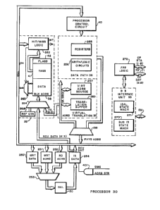
A detailed functional block diagram of one processor 30
used in the system is depicted in Fig. lB. With reference
... .
.. . .. .
.....
'
~79~
83-445
--11--
to Fig. ls, processor 30 includes a bus interface circuit 33
which connects to various control lines of bus 13
(collectively indicated by reference numeral 13A) and
transmits and receives signals over the various lines of the
bus as described below. The bus interface circuit also
connects to an internal IDAL bus 34 which transfers si~nals
to and from a cache 35, a data path 36, a memory management
unit 37, and a processor control circuit 40. A bus
interface circuit 33 for one embodiment of processor 30 will
be described below in connection with Fig. ~.
A number of registers also connect to the internal IDAL
bus 3~ and, under control of the bus interface circuit 33
transfers data between the internal IDAL bus 34 and DAI.
lines 50 of bus 13. Specifically, under control of the bus
interface unit 33, a write data register 250 and a write
address register 251 receive, respectively, write data and
the address o~ the location in memory 11 or input/output
units 12 in which the write data is to be stored. At
appropriate times, as described below, the bus interface
unit 33 enables the contents of these registers to be
transmitted through a multiplexer 253 onto the DAL lines 50
to perform a write operation. Similarly, under control of
.. . ' '
,. .;
' :,
~ 4 9904-108
the bus interface unit 33, a read address register 252 receives
an address of a location containing data to be read. At an
appropriate time, the bus interface unit 33 enables the contents
of the read address register 252 to be coupled through multi-
plexer 253 onto the DAL lines 50 to perform a read operation.
The read data is latched in an input register 254, also under
control of the bus interface unit 33. The bus interface unit 33
may enable the contents of the input register 254 to be coupled,
as RCV DAT received data signals, onto the internal IDAL bus 34.
The processor control circuit 40 decodes program
instructions which are retrieved from the memory 11 and in suc-
cessive processing cycles enables the data path 36 to perform
the arithmetic and logical operations which are required to exe-
cute the instruction. The data path 36 includes a set of regis-
ters 255 for storing data to be processed and arithmetic and
logic circuits 256 for performing the processing.
One embodiment of processor 30 uses ~irtual addresses
and provides virtual address translation circuits 37 for
.~ ~
~, . ..
. ~ , ................... . .
- . . ....
~28~2~L
83-445
-13-
translating the virtual addresses to physical addresses.
The virtual address translation circuits include a set of
source registers 257 which receive the virtual addresses
from other circuits in processor 30, most notably the data
path 36, and a translation buffer 260 which includes some
translation information. Translations are performed as
necessary under control of the processor control circuit 40.
Physical addresses are coupled from the translation circuits
37 onto the internal IDAL bus 34 through a multiplexer 261.
The data path 36 may also include physical addresses, and
provides a second source input for multiplexer 261. The
processor control circuit 40 controls multiplexer 261.
Cache memory 35 is a conventional information storage
circuit in a CPU 10. Cache memories are described in K.
Hwang and F. Briggs, Computer Architecture And Parallel
Processing (McGraw-Hill, 1984), Section 2.4, pp. 98, et seq,
and V. Hamacher, Computer Organization (McGraw-Hill, 1984),
Section 8.6, pp. 306, et seq. Cache memory 35 includes a
data storage area 38 comprising a plurality of storage
locations. The data storage area 38 is organized into
blocks, with each block containing two storage locations.
Each storage location stores one word of information, that
....
, :
., ' ,.
-14- 9904-108
is, the amount of information which may be transferred over bus
13 at one time. In one specific embodiment, a word of informa-
tion corresponds to four bytes, or thirty-two binary digits,
of information. Thus, each block can store eight bytes of
information.
Cache memory 35 includes hitlmiss logic circuits 262
which determines when a physical address generated by the vir-
tual address translation circuits corresponds to an address in
the cache memory 35. The low order portion of the virtual add-
1~ ress from the source registers 257, in one embodiment the VA
SRCE (8:3) signals, is coupled through a multiplexer 264 to
select one block in the data storage area, and the associated
tags 41 entry. The hit/miss logic circuits 262 then determine
whether the contents of the associated tags 41 entry corresponds
to the translated physical address. If there is such a corres-
pondence, the hit/miss logic generates an asserted HIT signal
which is transmitted to the bus interface unit 33. If the bus
interface unit 33 does not receive an asserted HIT signal, it
enables, in a conventional manner, an operation over bus 13 to
retrieve the contents of the addressed location. If
- ~ ~.: "
, : .
- .
,:
'' '
1287924
~ 3-445
-15-
the HIT signal is asserted, the bus interface unit 33 does
not enable the operation over bus 13, but instead allows the
data from the cache data storage area 38 to be transmitted
through a multiplexer 263 over the internal IDAL bus 34.
Generally, such data will be transmitted to the data path
36.
As will be appreciated by those skilled in the art, the
information stored in a block in the cache memory 35, when
it is received from the memory unit 11, is a copy of the
information stored in the memory unit 11. Each block in the
cache memory 35 has an associated tag 41 whose contents are
established by the bus interface circuit 36 to identify the
locations in the memory unit 11 from which the information
was copied. In addition, each block includes a stale flag
42 which is reset, or cleared,~by the bus interface circuit
to indicate whether or not the contents of the block are in
fact copies of the locations identified by the tag, that is,
whether or not the contents of the block are stale.
In one embodiment of cache memory 35 the data storage
area 38, tags 41 and flags 42 are dynamic memories. A
refresh counter ~, under control of the bus interface unit
.
.:
~2~37924
83-445
-16-
33 generates refresh addresses which are coupled through
multiplexer 264 to refresh the dynamic memories.
An instruction may contain one or more operand
specifiers which identify the location of the operand in the
registers in the data path 36, or which identify an address
which identifies the location of the operand in the virtual
address space. See, for example, U.S. Patent 4,236,206, for
a Central Processor Unit For Executing Instructions Of
Variable Length, issued to W.D. Strecker, et al., on
November 25, 1980. The processor control circuit 40, in
conjunction with the data path, decodes each operand
specifier to identify the locations of the operands, and
then proceeds to obtain them from the identified locations.
An operand specifier may itself contain the operand (that
is, the operand specifier may be a "literal"), the operand
specifier may identify one of the data path~s registers (not
shown) as containing the operand.
Alternatively, the operand may be in a location in the
program's virtual memory space, and~the operand specifier
may indicate how to determine that location. If the operand
is in the virtual memory space, the control circuit 40
enables the memory management circuit 37 to translate the
lX879Z4 83-445
-17-
virtual address to the physical address. After the physical
address of the operand has been obtained, the bus interface
33 obtains the operand. It first determines whether the
operand is in the cache memory 35. If the operand is in the
cache memory, the bus interface transmits the operand to the
data path 36. On the other hand, if the operand is not in
the cache memory 35, the bus interface circuit 33 transmits
a read request over the bus 13 to the memory 11 to retrieve
the operand. After all of the operands have been obtained,
the data path 36 may perform the operation required by the
instruction.
The operand specifier may also identify the location
into which processed data is to be stored. rrhe control
circuit 40 and memory management circuit 37 are used in the
same way as described above to determine the physical
address. If the processed data is to be stored in memory
11, the bus interface 33 performs the required write
operation over bus 13. In addition, if the physical address
corresponds to an appropriate tag in cache 35, the bus
interface 33 enables the data to be stored in the cache 35.
rrhe bus interface unit 33 includes a state machine 27.0,
which controls the transfer of data over bus 13, and an IDAL
~2~ 4
83-445
-18-
state machine 271, which controls the transfer of data over
internal IDAL bus 34. The bus interface unit also controls
an FPP logic circuit 272 which, in turn, controls
communications with the floating point processor 31. The
bus interface unit 33 will be described in more detail below
in connection with Fig.-~.
Operations Over Bus 13
The bus 13 includes a number of linés for transferring
signals representing information among the various units
connected to it. In particular, bus 13 includes DAL (31:0)
data address lines 50, which carry DAT data and ADRS address
signals. If the CPU 10, specifically the processor 30, is
initiating a transfer, making it the bus master for the
transfer, processor 30 first transmits the ADRS address
signals over the DAL ( 31:0) data address lines 50 and
contemporaneously transmits TR TYPE (2:0)~ transfer type
command signals on lines 52, which indicate whether the
transfer operation is a read or a write operation. A short
time later, sufficient to allow the ADRS address signals and
TR TYPE (2:0) transfer type command signals to settle, the
processor 30 then asserts an ADRS STR address s~robe signal
, .
'~ ' '' ,','~' .,
;`': .
83-495
--19--
on a line 51.
When the ADRS STR address strobe signal is asserted,
all of the other units connected to bus 13 receive and
decode the ADRS address and TR TYPE (2:0) transfer type
command signals, with the unit containing the location
identi~ied by the ADRS address signals being the responding
unit, or slave, for the transfer. If the transfer operation
is a write operation and the ADRS address signals identify a
location in the memory 11, the write buffer 23 is the slave
unit). A selected time later after the processor 30 asserts
the ADRS STR address strobe signal, it removes the ADRS
address signals and TR TYPE (2:0) transfer type command
signals from the respective lines.
If the transmitted TR TYPE ( 2:0) transfer type command
signals define a write operation, the master unit then
transmits data signals over the lines 50, and then asserts a
DATA STR data strobe signal on a line 53. The slave unit
then receives and stores the transmitted data. When the
data has been stored, the addressed unit then asserts a RDY
ready signal on a line 54 if the operation was completed
without error, or an ERR error signal on a line 55 if an
error occurred during the storage operation.
.
~l28~924
83-445
-20-
If, on the other hand, the transmitted TR TYPE (2:0)
transfer type command signals define a read operation, the
slave unit retrieves the data from the location identified
by the address signals, transmits them over the DAL (31:0)
data address lines 50, and transmits an asserted RDY ready
signal over line 54. In response, the processor 30 receives
the data and transmits an asserted DATA STR data strobe
signal over line 53.
In either a read or a write operation, after the slave
has asserted the RDY ready signal or the ERR error signal if
an error occurred during the transfer, the processor 30
negates the DATA STR data strobe signal. The slave unit
then negates the RDY ready or ERR error signal, and then the
processor 30 negates the ADRS STR address strobe signal to
complete the transfer.
Units connected to bus 13 other than processor 30 may
constitute bus masters and initiate transfers with the
memory 11 thereover. The input/output subsystem 12, and in
particular, their input/output controller 22 may become bus
master. To become bus master, input/output controller 22
asserts a DMR direct memory request signal over a line 56.
The processor 30 then asserts a DMG direct memory grant
.' ' . " ': ;~ :
- ;
.. .. . .. .... .... ... . . . .
7 ~ ~
83-445
-21-
signal on a line 57, which is received by the input/output
controller 22. At that point the input/output controller
initiates a transfer with the memory in the same way as
described above in connection with the processor 30. The
input/output controller maintains the DMR direct memory
request signal asserted until it has completed the transfer.
Thus, if the input/output controller requires multiple
transfers, it may maintain the DMR direct memory request
signal asserted until it has completed the transfers. While
the DMR direct memory request signal is asserted, the
processor 30 is in a stalled condition, that is, it monitors
the signals on the various lines of bus 13, but otherwise it
does not execute any instructions.
If the system includes multiple input/output subsystems
12, separate request signals by the input/output controllers
22 to become bus master are transmitted to the system
controller, which asserts the DMR direct memory request
signal and monitors the condition of the DMG direct memory
grant signal. ~hen the processor 30 asserts the DMG direct
memory grant signal, the system controller enables one o
the input/output controllers 22 to become bus master
according to any priority arbitration scheme~
;,
`` ~LZ~
60412~1-/96
Bus 13 also has a number of o~her lines whieh carry
status and control signals~ A line 60 carries CLK clock signals
which are used to synchronize operations in th~ system. The
various signals on bus 13 are timed in response to the CLK clock
signals.
A line 61 carries a CCTL cache control signal which has
two functions. The CCTL cache control signal is asserted by, for
example, an input/output controller 22 when it is bus master and
performing a write operation to memory 11. The input~output
controller 22 asserts the CCTL signal while it is ~ransmi~ting the
ADRS address signals on the DAL data address lines 50, TR TYPE
transfer type signals on lines 5~ and asserting the ADRS STR
address strobe signal on line 51. When the CCTL cache control
signal is asserted and the TR TYPE transfer type signals indlcate
a write operation to memory 11, the bus interface 33 checks the
contents of the tags 41 of all of the cache entries. If the ADRS
signals on the DAL data address lines 50 of bus 13 correspond ~to
the contents of a
~. - ,: ~ ; , ~
: ~ -
, ~
~l~87~
83-~45
-23-
tag 41, the bus interface 33 resets the S stale flag 42 for
that cache block.
The CCTL cache control signal is also asserted by
memory 11 to prevent the processor 30 from storing data in
the cache 35 that was requested during a read operation.
This may be used, for example, where memory 13 is a multi-
port memory, that is, if it is being shared by several
processors, with each processor accessing the memory 11 over
a separate bus, and the data being retrieved is from a set
of addressable storage locations that are available to all
of the processors. It is undesirable to have such data
stored in the cache 35 since another processor may update
the contents of the shared locations and, since the updates
are not over bus 13 they cannot be detected by the processor
30. If the processor 30 used such data from the cache, it
may not correspond to the contents of the appropriate
locations in memory. In connection with this use of the
CCTL cache control signal, the memory 11 asserts the CCTL
cache control signal contemporaneously with its transmission
of the data over the DAL data address lines 50, and
maintains the CCTL cache control signal asserted until it
removes the data.
~87~2~
83-445
-24-
Bus 13 also includes a line 62 which carries a CLR WRT
BUF clear write buffer signal. The CLR WRT BUF clear write
buffer signal is asserted by the processor 30 in response to
certain conditions internal to processor 30 which would not
be otherwise detectable outside of processor 30. For
example, the processor 30 asserts the CLR WRT BUF clear
write bu~fer signal when it executes an instruction which
causes it to switch process contexts or when it starts to
execute an interrupt service routine or an exception
routine. The CLR WRT BUF clear write buffer signal is
controlled by a field in microinstructions that are
generated by the processor control circuit 40 while
executing those instructions.
When the CLR WRT BUF clear write buffer signal is
asserted, the write buffer 23 determines whether it contains
data to be stored in memory 11. If it does not, it does
nothing. However, if the write buffer 23 does contain data
to be stored in memory 11, it asserts the DMR direct memory
request signal and continues to attempt to store its
remaining data in the memory 11. In response to the
asserted DMR direct memory request signal, the processor
asserts the DMG direct memory grant signal, which is ignored
,:
. . .
' ~:
,
.. . .
. . . :.
~2~379~
83-445
-25-
by the write buffer 23, and it also stalls. The write
buffer 23 maintains the DMR direct memory request signal in
the asserted condition until all of the data which it
contains has been properly stored in memory 11. If no error
occurs in the storage, the write buffer 23 then negates the
DMR direct memory request signal allowing the processor 30
to continue.
If an error does occur during a write to memory 11, the
write buffer 23 signals an error to the processor, allowing
the processor 30 to process routines to locate and correct
the error within the current context. This greatly
simplifies error recovery. If the processor is allowed to
switch contexts before an error is detected, it would be
difficult to determine the context which initially generated
the data. Error recovery is simplified if the context can
be identified, and so the write buffer 23 prevents the
processor from switching contexts until all of the data frcm
the current context has been properly stored in memory 11.
Transfers With Floating Point Processor 31
Processor 30 also is connected to floating point
processor 31 to (1) transfer the operation codes of floating
point instructions to the floating point processor 31 to
indicate the operation to be performecl, as describecl below
' ~
~Z87~3Z~
83-~45
-26-
in connection with Fig. 2A, (2) enable operand data to be
transferred to the floating point processor 31 for
processing as described in connection with Figs~ 2s and 2C
and (3) obtain processed data from the floating point
processor 31 as described in connection with Fig. 2D. The
processor 30 and floating point processor 31 are
interconnected by two sets of lines 70 and 71, lines 70
carrying CP STA (1:0) floating point status signals and
lines 71 carrying CP DAT ~5:0) floating point data signals.
The floating point processor 31 is also connected to several
lines of ~us 13, including DAL data address lines 50, line
60 for receiving the CLK signals, line 51 for receiving the
ADRS STR address strobe signal, line 54 for receiving the
RDY ready signal, line 55 for receiving the ERR error
signal, and line 57 for receiving the DMG direct memory
grant signal. The CP STA (1:0) floating point status
signals and CP DAT ~5:0) floating point data signals are
transmitted synchronously with the CLK signals on line 60.
While it is idle, the floating point processor 31
repetitively samples, synchronously with the CLK signal on
line 60, the conditions of the signals on the lines 70 and
71. When at least one of the lines 71 carries an asserteds
~ . ..
~ . .
' ~:
'
~X8~2~
83-445
-27-
level signal, the floating point processor 31 latches the
signals on those lines and the signals on lines 70. With
reference to Fig. 2A, when the processor 30 transmits an
instruction to the floating point processor 31, it transmits
at least a portion of the instruction's operation code to
th~ floating point processor 31 as CP DAT (5:0) floating
point data signals over lines 71 during an interval defined
by a selected number of ticks of the CLK clock signals.
During the interval, in synchronism with one of the ticks of
the CLR clock signals, the floating point processor 31
latches and stores the signals. At the end of the interval,
the processor 30 removes the signals from the lines 70 and
71.
The CP DAT l5:0) floating point data signals
transmitted over lines 71 are sufficient to identify a
floating point arithmetic operation to be performed, and
also identifies the number of operands to be used in the
operation. Concurrently with the transmission of the
operation information over lines 71, other information is
transmitted as the CP STA ¦1:0) floating point status
signals over lines 70 which provides further information
relating to floating point processing. In particular,
~Z~79~
83-445
-28-
floating point operands may be encoded in a number of
formats, termed data types, and information as to the format
of the operands is transmitted as CP STA (1:0) floating
point status signals over lines 70. In one embodiment, some
of the information as to the format of the operands is also
transmitted over the lines 71 along with the operation
information.
Upon receiving the operation code, the floating point
processor 31 decodes it to determine the operation to be
performed and the number of operands which are required.
The processor 30 (in response to sending the operation code)
and the floating point processor 31 (in response to
receiving the operation code) then go into a condition in
which the operands are transferred over DAL data address
lines 50. The data type information is used to identify to
the floating point processor 31 the format of each of the
operands. In connection with some operand formats, more
bits are required in some operand formats than can be
accommodated by a single transfer over the DAL data address
lines 50, and so multiple transfers are required to transfer
a single operand. The data type information thus also
~,.
' '` ~,
., ', ' ' '
; .
~37~;~4
83-445
-29-
indicates the number of transfers over DAL data address
lines 50 that are required to transfer each operand.
An operand may be stored in one of three sources,
namely, in the memory 11 (Fig. 1), in the cache 35, or in
the processor~s registers (sho~n in Fig. 3At in the data
path 36. The different operands required for a single
operation may also be stored in any of the three sources.
If multiple transfers over DAL data address lines 50 are
required to transfer a single operand, however, all of the
transfers are normally with respect to a single source.
Fig. 2B depicts the conditions of the signals that are
transmitted to retrieve an operand from memory and Fig. 2C
depicts the signals transmitted to transfer an operand from
the cache 35 or from registers in the data path 36. In
particular, Figs. 2B and 2C depict the conditions of the
signals to effect a single transfer over DAL data address
lines 50, and it should be recognized that multiple
trans~ers may be required for a single operand.
With reference to Fig. 2B, if an operand is in memory
11, the processor 30 initiates its retrieval from the memory
11. In particular, the processor 30 performs a read
operation, as described above, placing the ADRS address
, - ' ' " ' ' .,
~Z~379Z~
83-445
-30-
signals on the DAL data address lines 50 and asserts the
ADRS STR address strobe signal. Shortly thereafter, the
processor 30 places CP STA (1:0) floating point status
signals on lines 70 having the binary value zero, that is,
it negates both of the CP STA (1:0) floating point status
signals. In addition, the processor 30 transmits CP DAT
l5:0) floating point data signals on lines 71 in which the
CP DAT (5:4) floating point data signals contain an address
alignment code, which indicates how much of the data
transmitted over the DAL data address lines 50 is to be used
in the operand. The CP DAT ( O) floating point data signal is
asserted if the operand is a short literal on the DAL (5:0)
data address lines, and otherwise the CR DAT (1) floating
point data signal is asserted.
Since the floating point processor 31 has already
received the operation information in the procedure
described above in connection with Fig. ~A, it is in
condition to receive an operand. The asserted CP DAT (5:0)
~loating point data signal indicates to the floating point
processor 31 that it is to sample the signals on selected
lines of bus 13, in particular the line 51 which carries the
ADRS STR address strobe signal. The floating point
~l~87~24
83 445
-31-
processor 31 uses the asserted condition of the ADR5 STR
address strobe signal to determine that the operand is being
retrieved from the memory 11. If the ADRS STR address
strobe signal is asserted when it receives the asserted CP
DAT (5:0) floating point data signal, the floating point
processor 31 latches the data signals on the DAL data
address lines SO in response to the assertion by the memory
ll of the RDY ready signal on line 54. The processor 30
responds with the DATA STR data strobe signal to complete
the transfer.
It will be appreciated that, if the memory 11 responds
to a retrieval request with an asserted ERR error signal
instead of an asserted RDY ready signal, the floating point
processor 31 will not latch the transmitted data si~nals on
the DAL data address lines 50. The processor 30 performs
any required error recovery operations, such as retries,
which may be required and repeats the ope~ration dep~cted in
Flg. 2B.
Fig. 2C depicts a timing diagram useful in
understanding the transfer of an operand from the processor
30 to the floating point processor 31, whether the operand
is in the cache 35 or in a register in data path 36.
!~ ~
., ~ .
~L28~79~4L
60412-1796
In ei~her case, the processor places data signals on the DAL data
address lines 50 and CP DAT t5:0) floating point data signals
having the same encoding as described above in connection with
Fig. 2B, and negates both of the CP STA (1:0) floating point
status signals. These signals are maintained by the processor 30
for a selected number of ticks of the CLK clock signals. During
that interval, the floating point processor 31 latches the signals
on the DAL data address lines 50. If multiple transfers are
required over the DAL data address lines 50 to transfer an entire
operand, the sequence depicted in Fig. 2C is repeated.
If an operand's data type is such that multiple
transfers are required over DAL data address lines 50 to transfer
an entire operand, the processor 30, memory 11 and floating point
processor 31 repeat the operations depicted in Figs. 2B and ~C
untll a complete operand is transferred.
It will be appreciated that the sequence of operations
depicted in Fig. 2B is similar to the sequence of operations
depicted in Fig. 2C, with the followln~ difference. If the ADRS
STR address strobe siynal is asserted on line 51 when the CP DAT
~0 (5~0) floating point data slgnal is asserted, the
32
^.~
, ,
83-445
-33-
floating point processor 31 uses the asserted RDY ready
signal as an indication that the operand (or portion of the
operand) is then on the DAL data address lines 50. However,
if the ADRS STR address strobe signal is not asserted when
the CP DAT (5:0) floating point data signal is asserted, the
floating point processor 31 uses the assertion of the CP DAT
l5:0) floating point data signal as an indication that the
operand (or portion of the operand) is then on the DAL data
address lines 50. In both cases, the floating point
processor 31 latches the signals on the DAL data address
lines 50 in synchronism with the CLK clock signals on line
60, in the first case after receiving the RDY ready signal
and in the second case after receiving a CP DAT (5:0)
floating point data signal which is asserted.
After the operands have been transferred, the processor
30 and floating point processor 31 go into a condition in
which the processor 30 is prepared to receive the results
when the floating point processor 31 is prepared to send
them. Fig. 2D depicts a timing diagram which details the
sequence of operations used by the processor 30 and floating
point processor 31 to transfer the processed data to the
processor 30. The processed data comprises both the
,. . :"'~: '
:.
: ., ~ . . .
12~9Z~
83-445
-34-
condition codes, which indicates whether the result was a
negative or a zero and selected other facts concerning the
result, and data signals representing the value of the
computation performed by the floating point processor 31.
With reference to Fig. 2D, initially the processor 30
transmits a signal code over the lines 70 and 71 indicating
that it is ready to receive the processed data. In one
embodiment, the CP STA (1:0) floating point status signals
are both negated, and the CP DAT ( 3) floating point data
signal is asserted with the others negated. Thereafter, the
floating point processor 31 may transmit over lines 70 and
71.
When the floating point processor 31 is ready to
transfer the processed data, it transmits CP STA (1:0)
floating point status signals representing a code to that
effect, concurrently with CP DAT (5:0) floating point data
signals representing the condition codes. The floating
point processor 31 maintains these signals for a selected
number of ticks of the CLK clock signals, and then places
the data signals on the DAL data address lines 50, along
with a code on lines 70 and 71 to that effect. If multiple
transfers over DAL data address lines 50 to transfer the
.. ~
~ . '
~X~ 4
83-445
-35-
processed data signals, the floating point processor 31
transfers them synchronously with the CLK clock signals.
While the floating point processor 31 is processing
operands and before it has transmitted the results to the
processor 30, the processor 30 may assert the DMG direct
memory grant signal to allow input/output subsystem 12 to
engage in a transfer with memory 11. The floating point
processor 31 monitors the condition of line 57 after the
processor 30 has indicated that it is ready to receive the
processed data. If the DMG direct memory grant signal is
asserted on line 57 when the floating point processor 31 is
ready to return the processed data, the floating point
processor 31 delays returning the processed data until after
the DMG signal has been negated.
In addition, if an error occurs in, for example,
retrieving operands from memory 11, the processor 30 does
not indicate that wishes to receive processed data from the
floating point processor 31. The processor 30 does not
abort the operation of the floating point processor 31;
instead, when the processor 30 transmits a new operation
code to the floating point processor 31, the floating point
processor 31 operates on that operation code. It will be
. .
-'" `,.,'',',.' : '
,
1~8~2~
83-445
-36-
appreciated that the CP STA (1:0) floating point status
signals and CP DAT (5:0) floating point data signals
transmitted by the processor 30 over lines 70 and 71 to
indicate that it is ready to receive the processed data
should not correspond to any operation code, so as to allow
the floating point processor 31 to distinguish between them.
Bus Interface Circuit 33
A bus interface circuit 33 in one embodiment of the
processor 30 is depicted in Fig. 3. With reference to
Fig. 3, the bus interface circuit 33 includes a state
machine 270 which controls bus 13 (Fig. lA) and a second
state machine 271 which controls operations over internal
IDAL bus 34. The two state machines 270 and 271 operate
independently except for several flags and control signals,
as described below, which allow state machine 271 to
indicate to state machine 270 that operations over bus 13
are required, and response signals provi~ed by state machine
270 to indicate the completion of the operations to state
machine 271.
State machine 271, which controls the internal IDAL bus
34, receives input signals from a number of sources within
. . . .
~LZ8~
83-445
-37-
the processor 30, which are generally indicated by control
logic 273, from several terminals on bus 13, which are
generally indicated by pins 274 of bus 13, and from
microinstructions from control circuit 40 (Fig. lB). State
machine 271 transmits output signals to control number of
circuits within processor 30, including logic circuits 272
which control the transfers with the floating point
processor 31 and several signals which control the function
of the cache and the address input multiplexer 264
(Fig. lB). In addition, output signals from state machine
271 also control logic 276 which contains flags (not shown)
indicating that a read operation is pending, which is, in
turn, indicated by the condition of a RD REQ read request
signal, that a write operation is pending, as indicated by
the condition of a WRT REQ write request signal, and that a
transfer of operands from the processor 30 to the floating
point processor 31 is pending, as indicated by the condition
of a BRDCST REQ broadcast request signal.
Control logic 276, under control of the operating
system, also can determine whether certain information
received over bus 13 (Fig. lA) during a read operation is to
be stored in the cache 35 (Fig. lB). For example, the
''"' ' '
,:
.
.
.
~Z~37~2~
83-445
-38-
operating system may condition processor 35 to store all
information which it reads in the cache 35. Alternatively,
the operating system may not permit storing processor
instructions in the cache 35, and only permit storing of
data to be processed in the cache. Generally, however, the
operating system will not permit storing information which
is received from various control registers in the other
portions of the system depicted in Fig. lA in the cache 35.
The control logic 276 conditions a CACHE ACC cacheable
access signal to control the caching of the information
received over the bus 13.
As described above, an unit external to the processor
30 may also control whether the transfer is to be cached by
means of the CCTL cache control signal on line 61 (Fig. lA)
The state machine 271, directly or indirectly through
other control logic (not shown) also controls the loading of
write data and read and write addresses into latches 250
through 252, and also controls the transfer of read data
from input data latch 254 based on the conditions of the
signals on the pins 274.
State machine 270, which controls transfers over the
bus 13, receives the RD REQ read request, WRT REQ write
.
' ' ~'
- :
~L~87~
83-445
-39-
request, and ~RDCST REQ broadcast request signals from
control logic 276, as well as signals from bus pins 274, and
generates signals which are transmitted to logic circuits
277 which control the condition of several of the signals
comprising bus 13. In addition, the state machine 270
generates signals transmitted to control logic 2~0, which,
in turn, controls the operation of latches 250, 251, 252 and
254 and multiplexer 253 (Fig. lB) to allow signals to be
coupled onto and received from the DAL data/address lines 50
of bus 13. After a read operation has been completed, the
state machine 270 also asserts a CLR RD FLAGS clear read
flags signal which enables the control logic 276 to negate
the RD REQ read request signal.
With this background, the operation of the bus control
circuit 33 depicted in Fig. 3 will now be described. During
a write operation, as enabled by control circuit 40, if the
DMA OR WRT PND (DMA or write pending) signal is not asserted
by control logic 273, the state machine 271 first loads the
address of the location to be written into the write address
latch 251 (Fig. lB) and determines whether the location is
cached in the cache 35 (Fig. lB). If the DMA OR WRT PND
signal is asserted, either another unit in the system
. ..
, ; ~,,
. .
' . '' : '
.. ..
2~L
-40- 9904-108
depicted in Fig. lA is using the bus 13 or the state machine
271 has enabled a write address and data to be loaded into the
latches 251 and 250 (Fig. lB), respectively, which has not been
transferred over bus 13.
If the DMA OR WRT PND (DMA or write pending) signa] is
not asserted, a determination is made of whether the location to
be written is cached. If the location is cached, the entry in
cache 35 corresponding to that location must be updated with the
new data. To determine whether the location is cached, the state
machine 271 generates CACHE FTN (1:0) cache function signals
enabling the cache to be read and CACHE ADRS (1:0) signals enabl-
ing the multiplexer 264 to use the physical address generated by
the virtual address translation circuit 37. During this opera-
tion, an IDAL CACHE XMIT cache transmit signal is negated to
inhibit the data from the cache to be coupled onto the internal
data bus 34. If the location is cached, the HIT signal will be
asserted by hit/miss logic circuits 262, which will be reflected
in the condition of the MISS signal from control logic 273.
If the MISS signal is not asserted, the location to be
written is cached. In response to a negated MISS signal,
' .~
.
~l28~79~4
83-445
--41--
the state machine 271 generates CACHE FTN (1:0) cache
function signals enabling a cache write operation and CACHE
ADRS (1:0) cache address signals enabling the multiplexer
264 to use the address from the virtual address translation
circuit 37. Simultaneously, the data written into the cache
entry is stored in the write data latch 250 ( Fig . lB) and
the flags in the control logic are conditioned to generate
an asserted WR REQ write request signal. During this
operation, the MBOX STALL signal is asserted to disable the
virtual address translation circuitry from operating.
On the other hand, if the MISS signal is asserted, the
location to be written is not cached. In response to the
asserted MISS signal, the state machine enables the write
data to be latched in the write data latch 250 (Fig. lB) and
the WRT REQ signal to be asserted by control logic 276. In
addition, the CACHE ADRS (1:0) cache address signals are
conditioned to increment a refresh counter 262 (Fig. lB) and
enable multiplexer 264 to couple the address to the flags
42, tags 41 and data store 38 (Fig. lB) to permit them to be
re~reshed. During this operation, the MBOX STALL signal is
also asserted to disable the virtual address translation
,
: , ' . '
: ~,`' ~, ',,
., , , " , ~ ,
,
:';
`` -' JLZ~37~
-42- 9904-108
circuitry from operating to prevent it from producing another
physical address.
After the write operation is completed, the DMA OR WRT
PND (DMA or write pending) signal is negated. This permits
another address and write data to be loaded into the latches 250
and 251 (Fig. lB). The refresh operation is also enabled.
The operations performed or enabled by state machine
271 during a read operation depend on whether the requested
information is an instruction or data and whether or not the
requested information was in cache 35 (Fig. lB). The information
is in the cache if the location identified by the address is
cached and if there is no parity error on either the tag 41 or
the data 38 (Fig. lB), which would render the cache entry unusable.
A read operation may be required to retrieve an instruction, in
which case the control logic 273 asserts an IB REQ instruction
buffer request signal. Otherwise, control circuit 40 asserts an
RD read signal. If the required information is not in the cache
35, the control logic 273 also asserts a READ MISS signal. The
READ MISS signal is the complement of the HIT signal depicted in
Fig. lB.
~,
~28~
83-445
~43-
In response to an asserted RD read signal from ~ontrol
circuit 40 or the assertion of the IB REQ instruction buffer
request signal, the state machine 271 generates CACHE FTN
~1:0) cache function signals which enable a cache read, and
CACHE ADRS (1:0) cache address signals which enable
multiplexer 264 (Fig. lB) to use the address from virtual
address translation logic 37. Simultaneously, the state
machine 271 asserts the A~M ADRS STR arm address strobe
signal which enables the address from the virtual address
translation logic 37 to be loaded into the read address
latch 252. If the operation was in response to the IB REQ
signal, the state machine 271 also asserts an INIT IB REQ
initiate instruction buffer request signal, which enables
the control logic 273 to set a flag which, in turn, enables
the assertion o~ a PREV IB REQ previous instruction buffer
re~uest signal. If the information is in the cache 3S, the
state machine 271 allows the inEormation to be coupled from
the cache 35 onto as described above in connection with
\~,
Fig. ~, and the operation terminates.
If the information is not in the cache 35, and if the
DMA OR WRT PND ~DMA or write pending) signal is asserted,
the state machine 271 asserts both the STALL and MBOX STALL
. ', '' `' '' '
~2~7~ 4
83-445
-4~-
signals to stall the processor 30, and CACHE ADRS (1:0)
signals allowing a refresh operation. The stall permits the
write operation to be completed before proceeding with the
read operation.
If the DMA OR WRT PND (DMA or write pending) siqnal is
negated, the read operation proceeds. The state machine 271
enables the control logic 276 to assert the RD REQ read
request signal. The state machine 271 then monitors the
C~CHEABLE, CCTL cache control, RDY ready and ERR error
signals to determine the end of the read operation. If the
CACHEABLE or CCTL cache control signals indicate that the
information should not be cached, there is one transfer over
bus 13. On the other hand, if the information is to be
cached, two transfers are required, one for each word in the
cache entry L}~ t. Since in one specific embodiment the
second least significant address bit identifies the word
being retrieved, during the second retrieval the second
address bit in the read address re~gister is inverted to
identify the second word to be retrieved. Thus, the words
may be retrieved in reverse order in which they are located
in the addressable locations in the memory 11.
~`
,
. --~
9~
83-445
-45-
If the transfer is to be cached, when the RDY ready
signal is received, if the DAL PAR ERR parity error signal
is not asserted, indicating no parity error in the received
information, the state machine 271 enables the multiplexer
264 (Fig. lB) to use the address from the virtual address
translation circuit to select an entry in the cache 35, and
enables the information to be loaded into either the
selected high or low word. The word in the cache 35 into
which the information is to be loaded depends on the
condition of *~e VA (2) virtual address bit (scc ~ig. 5~.
The information is then coupled to the data path 36
~Fig. ls).
If the DAL PAR ERR parity error signal is asserted, or
if the ERR error signal is asserted on line 55 (Fig. lA)
indicating an error response by the other unit engaged in
the transfer, the operation depends on whether the PREV IB
REQ previous instruction buffer request signal is asserted.
I~ it is, the control circuit 40 (Fig. lB) is notified by an
asserted IB FILL ERR instruction buffer fill error signal to
permit it to take corrective action. If the PREV IB REQ
previous instruction buffer request signal is not asserted,
the STALL and MBOX STALL signals are asserted to stall the
;~
~28~g24
83-445
-46-
processor 30, and a TRAP REQ trap request signal is
asserted, which allows the processor control circuit 40 to
perform selected recovery operations.
If the received information is to be cached, and if
neither the ERR error signal or the DAL PAR ERR parity error
signal is asserted as the data is received, the state
machine 271 proceeds to enable a second word to be received
and stored in the cache 35. If the second word is properly
received, it is stored in the cache 35 as described above.
The state machine 271 generates CACHE ADRS(1:0) cache
address signals which enable the multiplexer 264 to use the
address from the virtual address translation circuit 37 and
CACHE FTN (1:0) cache function signals enabling the second
word to be stored in the cache entry. The state machine 271
does not, however, enable the information to be transferred
to the data path 36.
On the other hand, if the ERR error signal or if the
DAL PAR ERR parity error signals are asserted, the MBOX
STALL signal is asserted to stall the virtual address
translation circuit 37 and the entry in the cache into which
the first word was written is marked invalid. At the same
time, the CACHE ADRS (1:0) signals are conditioned to enable
.
-` ~ 2~379'~:~
83-445
-47-
multiplexer 264 to use the refresh address from refresh
counter 262 to refresh the contents of cache 35, and to
increment the counter.
State machine 271 enables refresh operations to be
performed whenever the state machine 271 is not enabling
in~ormation to be written into or read out of the cache 35.
To enable operations to occur, the state machine 271
generates CACHE ADRS signals which enable the multiplexer
264 to use refresh address signals from the refresh counter
262 to refresh the contents of the storage circuits 38, 41
and 42 (Fig. lB) in a conventional manner.
State machine 271 also enables entries in cache 35 to
be invalidated in response to a DMA INV REQ invalidate
request signal from control logic 273. AS described above
in connection with Fig. lB, this signal is generated in
response to the coincidence of an asserted CCTL cache
control signal and an asserted ADRS STR address strobe
signal, when both signals are asserted by other units in the
system depicted in Fig. lA. This occurs when the other
units are performing DMA (direct memory access) operations
with memory ll, and so the DMG direct memory grant signal
will be asserted. If another unit transfers data to a
:, ,
...
. , ' ~ .
, .. : . . .
~ z~37924
~ 3-445
-48-
location in memory 11 which is cached in cache 35, the cache
entry must be marked invalid. With reference to Fig. lB, in
response to the coincidence of the DMG and ADRS STR address
strobe signal, an AND gate 401 enables the input data latch
254 to latch the signals, which in this case are address
signals, on DAL data/address lines 50.
In response to the DMA INV REQ invalidate request
signal, the state machine 271 first attempts to perform a
read operation of cache 35 using the address in the input
data latch 254, without allowing the data from the cache to
be coupled onto the internal bus 34. If the MISS signal is
asserted, the location is not cached, and nothing further
occurs.
However, if the MISS signal is negated, the location
identified by the address in the input data latch 254 is
cached, and the state machine initiates ~ cache invalidate
operation. In this, it generates CACHE FTN (1:0) cache
function signals which enable an invalidation operation, and
CACHE ADRS (1:0) cache address signals which enable the
multiplexer 264 to use the contents of the input data latch
in the invalidation.
, . :" " ~'
~ 2~379~ a~
83-445
-49-
State machine 270 operates in response to the CCTLcache control, DMR direct memory request, RDY ready and ERR
error signals from bus 13, RD REQ read request, WRT REQ
write request, BRDCST REQ broadcast request, and CACHE ACC
cacheable access signals from control logic 276, and INH DMA
inhibit direct memory access and ARM RD REQ arm read request
signals from state machine 271. If the state machine 270
receives an asserted DMR direct memory request signal,
indicating that another unit in the system depicted in
Fig. lA wishes to per~orm a transfer over bus 13, unless the
INH DMA inhibit DMA or BRDCST REQ broadcast request signals
are asserted, it negates the DIS DMG disable direct memory
grant signal, which, in turn, enables control logic 277 to
assert the DMG direct memory grant signal. The asserted DMG
direct memory grant signal enables another unit to perform a
transfer over bus 13. In addition, the state machine 270
asserts the DATA IN signal which enables DAL control logic
280 to condition the DAL data/address lines 50 to permit
other units in the system to use them. The state machine
270 also asserts the TRI-STATE STR signal to enable control
logic 277 to permit other units to use the DATA STR data
strobe, ADRS STR address strobe, and TR TYPE transfer type
signals.
.~ ,. ..
, . .
~ ~79~4 83-445
-50-
Alternatively, if no other unit in the system is to
perform a transfer over the bus 13, the state machine 270
enables transfers thereover in response to the RD REQ, WRT
REQ, and BRDCST REQ broadcast request signals from control
logic 276. If the WRT REQ write request signal is asserted,
indicating a write address and write data in latches 251 and
250 (Fig. lB) respectively, if the DMR signal is not
asserted, the state machine 270 generates DAL CONT (1:0)
tDAL contents) signals which enable the multiplexer 253 to
couple write address from latch 251 onto the DAL
data/address lines 50. Simultaneously, the state machine
270 asserts an ADRS STR EN address strobe enable signal
which, in turn, enables the control logic 277 to assert the
ADRS STR address strobe signal.
Next, the state machine 270 generates DAL CONT (1:0)
(DAL contents) signals which enable multiplexer 253 to
couple the contents of the write data latch 250 onto DAL
data/address lines 50. Simultaneously, the state machine
270 asserts a DATA STR EN data strobe enable signal, which
enables the control logic 277 to assert the DATA STR data
strobe signal. Thereafter, the state machine waits until
the RDY ready or ERR error signals are asserted. If the
: . .
~LX87924
83-445
-51-
asserted RDY signal is received, the operation terminates by
negating the ADRS STR EN address strobe enable and DATA STR
EN data strobe enable signals, which in turn, enables
control logic 277 to negate the ADRS STR address strobe and
DATA STR data strobe signals, respectively, and the control
logic 276 is enabled to negate the WRT REQ signal.
On the other hand, if the asserted ERR error signal is
received, the state machine 270 performs a retry attempt, in
which it generates DAL CONT (1:0) (DAL contents) signals
which enable multiplexer 253 to couple the write data
signals from latch 250 onto DAL data/address lines 50.
If both the RDY ready and ERR error signals are
asserted, a retry is signaled, and the transfer is attempted
again.
If no other operation is occurring, the state machine
270 generates DAL CONT (1:0) (DAL contents) signals which
enable multiplexer 253 to couple the contents of the read
address latch 252 onto the DAL data/address lines 50. This
permits the state machine 270 to initiate a read operation
quickly when other signals and conditions permit a read
operation to occur. During a read operation, when the RD
. .
- ' ' ,
79~
83-445
-52-
REQ read request signal is asserted, the state machine 270
asserts the ADRS STR EN address strobe enable signal, which,
in turn, enables the control logic 277 to assert the ADRS
STR address strobe signal. The state machine 270 then
asserts the DATA IN data in signal which enables control
logic 280 to condition the DAL data/address lines 50 to
enable other units in the system to use them.
Simultaneously, the state machine asserts the DATA STR EN
data strobe enable, which, in turn, enables the control
logic 277 to assert the DATA STR data strobe signal.
The next operations depend on whether the CACHE ACC
cacheable access signal is asserted by control logic 276.
If the signal is asserted, the retrieved data is cacheable,
and so two words are read over bus 13. On the other hand,
if the CACHE ACC cacheable access signal is not asserted,
the retrieved data is not cacheable and only one word is
read over bus 13. If the CACHE ACC cacheable access signal
is` not asserted, the state machine 270 asserts a RD DATA LAT
read data latch signal which, when asserted, enables the
input latch 254 ( Fig. lB) to receive the signals on DAL
data/address lines 50. When the RD DATA LAT read data latch
signal is thereafter negated, the signals are latched by the
'''
': : ~.,,:
g;~:4
83-445
-53-
input latch. The state machine 270 negates the RD DATA LAT
read data latch signal in response to the asserted RDY ready
signal if the ERR error signal is negated and asserts the
CLR RD FLAGS clear read flags signal. In response to the
asserted CLR RD REQ signal, the control logic 276 negates
the RD REQ read request signal.
On the other hand, if the CACHE ACC cacheable access
signal is asserted, a read operation is performed as
described above. If the CCTL cache control signal is not
asserted when the data is latched in the input data latch, a
second operation is also performed. If, on the other hand,
the CCTL cache control signal is asserted, indicating that
the other unit engaged in the transfer is precluding caching
of the data, the second operation is not performed.
The state machine 271 uses the IN~ DMA inhibit direct
memory access signal to inhibit state machine 270 from
asserting the DMG direct memory grant signal in response to
the receipt of a DMR direct memory request signal from other
units. The INH DMA inhibit direct memory access signal is
asserted during certain transfers with the floating point
processor 31 (Fig. lA).
. , ' ~ ~ ... , :
~ 2~79~4 83-445
-54-
The RD BRDCST read broadcast and BASIC BRDCST basicbroadcast signal from control circuit 40 enable the state
machine 271 to transfer floating point operand information
from cache 35 or registers 255 in data path 36 (see
Fig. lB). The control logic 276 is also enabled to assert
the BRDCST REQ broadcast request signals to, in turn, enable
the state machine 270 to transfer this information as
described above. The state machine 271 also enables control
logic 273 to set a flag which asserts an FPP PND floating
point processor pending signal. The state machine 271
asserts an SIG FPP signal floating point processor signal to
indicate to FPP interface circuitry 272 that it is ready to
receive the results of a floating point operation from the
floating point processor 31. When the condition codes are
ready, as described above, the interface circuitry 272
asserts a CP OK signal, and when the result data is ready,
it asserts a CP RDY ready signal. In response to the CP RDY
ready signal, state machine 271 enabies state machine 270 to
receive the result data. If the floating point processor 31
signals an error, the interface circuitry 272 asserts a CP
ERR error signal. In response to the CP OK, CP RDY or CP
ERR signal, the state machine 271 enables the flag
.
- ,, ' .:' '
~ .
', ',
~ 2 87 g~ ~ 83-445
-55-
controlling the FPP PND floating point processor pénding
signal to be reset, thereby negating the signal.
The bus interface circuit 33 provides a number of
benefits. First, the use of two state machines 270 and 271,
each controlling different operations and communicating
through flags, simplifies the circuitry considerably.
Furthermore, the state machine 271 enables refreshing
o the cache 35, permittins use of dynamic memory elements
therein. This reduces the physical size of the cache, or
alternatively facilitates providing more cache storage in
the same area, as has been the case in the past.
Furthermore, it will be appreciated that the bus
interface circuit 33, in retrieving cachable data, first
retrieves the data which is required by the program, and
then retrieves the other word for storage in the cache
entry. In prior systems, the data words were retrieved in
the order in which they were stored in memory, and so the
first data word may not have been the one immediately
required by the program. This delayed resumption of
processing until the second word was retrieved.
, ..
" ~:
-: '
. :
... .
~.2~g~4
~3-445
-56-
In addition, the bus interface circuit 33 permits read
operations to be initiated, to the extent that a read
address is generated and latched in the read address latch
252, while a write operation is pending. The read operation
is not completed until the pending write operation is
completed, but when the write operation has been completed,
the read address can be transmitted immediately.
Finally, the bus interface circuit also permits cache
entries to be invalidated, by direct memory access operation
performed by other units in the system depicted in Fig. lA,
independently of whether read or write operations have been
set up in processor 30. That is, the cache entry invalidate
operation can take place, in response to a DMA address
received in input latch 254, while write data and a write
address are latched in the respective latches 251 and 250
(Fig. lB) and a read address is latched in latch 252. This
simplifies the invalidation process~.
The foregoing description has been limited to a
specific embodiment of this invention. It will be apparent,
however, that variations and mod1fications may be made to
the invention, with the attainment of some or all of the
:
advant~ges of ~he inventioA. The~-fore, it is the object of
.
.,:: : . .. : :
: .
,~ :-... : ..
,
: .
., : . .: ~, ~ ,
, ' : :'. ~
` ~2~7~ 83-445
-57-
the appended claims to cover all such variations and
modifications as come within the true spirit and scope of
the invention.
:`
.
.
, '~ . ,,