Note: Descriptions are shown in the official language in which they were submitted.
3848~i
IMPLEMENTATION AND CONTROL Of FILTERS
TECHNICAL FIELD
The present invention may be related to the technical field of irnpiementatisn
and control of electrically controllable active filters, where implementation
and control thereof is achieved with the aid of a differential gain stage
especially invented for this purpose. The differential gain stage can be included
in high-pass filters as well as low-pass filters of the first and second order and
in an oscillator for controlling such filters.
~ACKGROUND ART
Several different types of electrically controllable active filters are well
known, as well as their design and manufacture in the form of integrated
circuits. It is further known to tune active filters with the aid of an outside
phase-locked loop which is locked to a given frequency. A general description ofthe design and control of active electrical filters for realization in the form of
integrated circuits is presented in the article "Analog integrated filters or
continous-time filters for LSI and VLSI", REVUE DE PHYSIQUE APPLIQUEE,
January 1987, No. 1, pp 3-14. Further information as to the design and control
of active filters is given in the references found on pages 13 and 14 in the
article.
The US patents 4288754 and 4306198 teach the use of differential amplifiers
with groups o-F series-connected diodes in the design of electrically controllable
active filters.
From the US patent 4379Z68 it is known in other applications than filters also
to use differential amplifiers with groups of series-connected diodes.
DISCLOSURE OF INVENTION
Up to now it has been a problem to design and control electrically controllable
active filters for high frequencies in the order of magnitude 500 MHz. No least
~L
~ ~ ~3 8 ~
has been a prvblem to deslgn and achleve control of such fllters
so that they can be manufactured at low cost In the form of Inte-
grated clrcults. It has also been a problem to deslgn and con-
trol suct1 fllters so that they can be tuned over a comparatlvely
large frequency range.
One obJect of the present Inventlon Is to enable Imple-
mentatlon and control of electrlcally controllable actlve fllters
for the VHF and UHF bands, preferable for frequencles of the
order of magnltude 500 MHz.
A somewhat dlfferent obJect of the present Inventlon Is
to achleve Implementatlon and controJ of elec~rlca~ly control-
lable actlve fllters for frequencles of the order of magnltude
500 MHz, such that manufacture can be carrled out easlly and
cheaply In the form of Integrated clrcults, preferably wlth the
use of blpolar technlque.
A further obJect of the present Inventlon Is to enable
the Implementatlon and control of electrlcally controllable
actlve fllters for the VHF and UHF bands, preferably for frequen-
cles of the order of magnltude 500 MHz, where such fllters can be
electrlcalIy tuned over a c3mparatlvely large frequency range.
A stlll further obJect of the present Inventlon Is to
enable the Implementatlon and tunln~ of an electrlcally control-
lable actlve fllter for the VHF and UHF bands, where thls fllter
only requlres a supply voltage of about 5 volts.
These and other obJects are achleved In accordance wlth
the Inventlon by a dlfferentlal galn stage speclally Invented for
the purpose, belng utlllzed $or the Implementatlon and control of
the flIters. Thls stage has two ampllflcatlon ~omponents, at
least two groups of serles-connected dlode components and at
3~ least one current generator connected to each other In a certaln
way, whereby the dlfferentla~ galn stage wlll be part~cularly
~ ~884~
suitable for the purpose.
A filter implemented according to the invention includes at least
one differential gain stage. Filters of the second higher orders
can include two or more differential gain stages. An oscillator
for controlling a filter via an outside phase-locked loop can
contain three differential gain stages.
According to one aspect thereof, the present invention provides
an active filter comprising a first differential gain stage with
a first differential input and a first differential output, said
first differential gain stage including two amplification
components, at least four diode components, a capacitive
component connected in parallel with the differential output of
said differential gain stage, and a current generator, said
amplification components having substantially egual relationship
between current and forward voltage drop, each amplification
component having its control electrode connected in counterphase
directly to the first di~ferential input, so that the difference
between the potentials on the control electrodes increases with
increased voltage across the first differential input, said diode
components each having substantially the same relationship
between current and forward voltage drop as the amplification
components, said diode components being series-connected in
groups so that there are at least two series-connected diode
components in each group, of which groups a first is connected to
a first of the amplification components, while a second group is
connected to a second of the amplification components, said
second group lncluding as many diode components as the first
group, said first and second amplification components being
coupled in counterphase directly to the first differential
output, such that the magnitude of the voltage across the first
differential output varies with the difference between the
forward voltage drops across the first and the second
amplification components, and wherein the first group and second
group of diode components are connected in counterphase directly
- 3 -
9 ~ 34~
to the first differential output, said current generator being
connected to one of the amplification components and the groups,
such that for an unloaded first differential output the magnitude
of the current through the first group substantially agrees with
the magnitude of the current through the first amplification
component, while the magnitude of the current through the second
group substantially agrees with the magnitude of the current
-through the second amplification component. Suitably the first
amplification component together with the first group are
included in a first series circuit, while the second
amplification component together with the second group are
included in a second series circuit, and wherein the first and
second series circuits are connected in parallel to said current
generator such that the sum of the current through the first and
second amplification components is substantially constant.
In another aspect thereof, the invention provides a second
differential gain stage with a second differential input and a
second differential output, said second differential gain stage
including two amplification components, at least four diode
components and at least one current generator, said amplification
components of said second stage having substantially equal
relationship between current and forward voltage drop, eac~
second-stage amplification component having its control electrode
connected in counterphase directly to the second differential
input, so that the difference between the potentials on the
control electrodes increases with increased voltage across the
second differential input, said second-stage diode components
each having substantially the same relationship between current
and forward voltage drop as the second-stage amplification
components, said diode components being series-connected in
groups so that there are at least two series-connected diode
components in each group, of which groups a first is connected in
series with a first of the second-stage amplification components,
while a second group is connected in series with a second of said
amplification components, said second group including as many
- 3a -
348~;
diode components as the first gxoup, said first and second
amplification components being coupled in counterphase directly
to the second differential output, such that the magnitude of the
voltage across the second differential output varies with the
difference between the forward voltage drops across the first and
the second second-stage amplification components, further wherein
at least one of the first and second groups, and third and fourth
groups, respectively, of diode components are connected in
counterphase directly to the second differential output, said
fourth group containing in appropriate cases as many dlode
components as the third group, further including at least one
second-stage current generator connected to at least one of the
second-staye amplification components and the second-stage
groups, such that for an unloaded second differential output the
magnitude of the current through the first and four$h groups,
respectively, substantially agrees with the magnitude of the
current through the first second-stage amplification component,
while the magnitude of the current through the second and third
groups, respectively, substantially agrees with the magnitude of
the current through the second of the second-stage amplification
components, and further including a pair of substantially like
series circuits, each connected to a further current generator
and also each to its own series circuit in the first differe~tial
gain stage in the same way as the first capacitiv~ component,
said pair of series circuits each having an amplification
component with a control electrode, and wherein the output of the
first differential gain stage is connected to the input of the
second differential gain stage, and the output of the second
differential gain stage is connected to the control electrodes of
the amplification components in said pair of series circuits.
Suitably a filter further includes control means for synchronous
control of the currents through the current generators of ~he
differential amplifier stages.
The present invention further provides an oscillator including
the aforesaid filter and including a second and a third
- 3b -
384~s;
differential gain stage each with a differential input and a
differential output, said second and third differential gain
stages each including: two amplificat.ion components, at least
four diode components and at least one current generator, said
amplification components in a stage having substantially equal
relationship between current and forward voltage drop, each
ampliflcation component in a stage having its control electrode
connected in counterphase directly to the differential input of
the stage in question, so that the difference between the
potentials on the control electrodes increases with increased
voltage across the differPntial input of that stage, said diode
components in a stage each having substantially the same
relationship between current and forward voltage drop as the
amplification components in the same stage, said diode components
in a stage being series-connected in groups so that there are at
least two series-connected diode components in each group, of
which groups a first is connected in series with a first of the
amplification components in the stage, while a second group is
connected in series with a second o~ the amplification components
in the stage, said second group including as many diode
components as the first group, said first and second
amplification components in the same stage being coupled in
counterphase directly to the first differential output of that
stage, such that the magnitude of the voltage across the
differential output of that stage varies with the di*ference
between the forward voltage drops across the first and the second
amplification components in that stage, and wherein one of the
first and second group, a~d the third and fourth group,
respectlvely, of dlode ccmponents in a stage are connected in
counterphase directly to the differential output of that stage,
said fourth group containing as many diode component~ as the
third group, there being at least one current generator connected
to at least one of the amplification components and the groups in
the same stage, such that for an unloaded differential output the
magnitude of the current through the first and fourth groups,
respectively, substantially agrees with the magnitude of the
- 3c -
~8~86
current through the first amplification component, while the
magnitude of the current through the second and third groups,
respectively, substantially agrees with the magnitude of thP
current through the second amplification component in the same
stage, a second capacitive component connected in parallel to the
differential output of the second stage, a third capacitive
component connected in parallel to the differential output of the
third stage, and wherein the differential ou-tput of the first
stage is connected to the differential input of the second stage,
lo the differential output of the second stage is connected to the
differential input of the third stage and the differential output
of the third stage is connected to the differential input of the
first stage.
The present invention further prov1des an amplifier circult for
use in active filters, said device comprlsing a first
differential gain stage with a first differential input and a
first differential output, said first differential gain stage
including two amplification components, at least four diode
components and a first current generator, said amplification
components having substantially equal relationship between
current and forward voltage drop, each amplification component
having its control electrode connected in counterphase directly
to the first differential input, so that the difference between
the potentials on the control electrodes increases with increased
voltage across the first differential input, said diode
components each having substantially the same relationship
between current and forward voltage drop as the amplification
components, said diode components being series connected in
groups so that there are at least two series connected dlode
components in each group, of which groups a first is connected in
series with a first of the amplification components, while a
second group is connected in series with a second of the
amplif1cation components, said second group including as many
diode components as the first group, said first and second
amplification components being coupled in counterphase directly
- 3d -
~, .. .
1 ~ ~ 8 ~
to the first differential output, such that the magnitude of the
voltage across the first differential output varies with the
difference between the forward voltage drops across the first and
the second amplification components, further including a third
and fourth group of diode components connected in counterphase
directly to the first differential output, said fourth group
containing as many diode components as the third group, said
first current generator being connected to at least one of the
amplification components and the groups, such that for an
unloaded first differential output -the magnitude of the current
through the fourth group substantially agrees with the magnitude
o~ the current through the first amplification component, while
the magnitude of the current through the third group
substantially agrees with the magnitude of the current through
the second amplification component. Suitably the first
amplification component together with the first group of diode
components are included in a first series circuit, while the
second amplification component together with the second group of
diode components are included in a second series circuit, and
wherein the first and second series circuits are connected in
parallel to said current generator such that the sum of the
currents through the first and second amplification components is
substantially constant, further wherein the first series circuit
and the third group of diode components are connected in parallel
to a second current generator such that the sum of the currsnts
through the first amplification component and the third group is
substantially c~nstant for an unloaded differential output, and
the second series circuit and the fourth group of diode
components are connected in parallel to a third current generator
such that the sum of the currents through the second
amplification component and the fourth group is substantially
constant for an unloaded first differential output, and wherein
the first, second and third current generators are adapted to
generate substantially equal currents. Desirably said filter
3~ further includes a capacltive component connected in parallel
with the differential output of the differential gain stage.
- 3e -
~X8~34~36
In one embodiment of the invention the filter also includes a
second differential gain stage with a second differential input
and a second differential output, said second differential gain
stage including two amplification components, at least four diode
components and at least one current generator, said amplification
componen~s of said second stage having substantially equal
relationship between current and forward voltage drop, each
second-stage amplification component having its control electrode
connected in counterphase directly to the second differential
1~ input~ so that the dlfference between the potentials on the
control electrodes increases with increased voltage across the
second differential input, said second-stage diode components
each having substantially the same relationship bet~een currPnt
and forward voltage drop as the second-stage amplification
components, said diode components being series-connected in
groups so that there are at least two series-connected diode
components in each group, of which groups a first is connected in
series with a first of the second-stage amplification components,
while a second group is connected in series with a second of said
amplification components, said second group including as many
diode components as the first group, said first and second
amplification components being coupled in counterphase directly
to the second differential output, such that the magnitude of the
voltage across the second differential output varies with the
difference between the forward voltage drops across the first and
the second second-stage amplification components, ~urther wherein
a third and a fourth group of second-stage diode components are
connected in counterphase directly to the second differential
output, said fourth group containing in appropriate cases as many
diode components as the third group, further including at least
one second-stage current generator connected to at least one of
the second-stage amplification components and the second-stage
groups, such that for an unloadsd second differential output the
magnitude of the current through the first and fourth groups,
respectively, substantially agrees with the magnitude of the
current through the first second-stage amplificatlon component,
- 3f -
~X88~86
while the magnitude of the currPnt through the second and third
groups, respectiveiy, substantially agrees with the magnitude of
the current through the second of the second-stage amplification
components, and further lncluding a pair of substantially llke
series circuits, each connected to a further current generator
and also each to its own series circuit in the first differential
gain stage in the same way as the first capacitive component,
said pair of series circuits each having an amplification
component with a control electrode, and wherein the output of the
first differential gain stage is connected to the input of the
second differential gain stage, and the output of the second
differential gain stage is connected to the control electrodes of
the amplification components in said pair of series circuits.
Desirably said filter further includes control means for
synchronous control of the currents through the current
generators of the dlfferential amplifier stages.
The present invention again provides a large pass filter
accompanying the amplifier circuit and further includes a
capacitive component connected to each of the series connected
circuits on the opposite side of the respective amplification
component as is the differentlal output of the differential gain
stage.
The present invention also provides an amplifier circuit for use
in active filters, said device comprising a first differential
gain stage wlth a first dif~erential input and a first
differential output, said first differential gain stage including
two amplifi~ation components, at least four diode components and
a plurality of current generators, said amplification components
having substantially equal relationship between current and
forward voltage drop, each amplification component having its
control electrode connected in counterphase directly to the first
differential input, so that the difference between the potentials
on the control electrodes increases with increased voltage across
the first differential input, said diode components each having
- 3g -
~Z88~86
substantially the same relationship between current and forward
voltage drop as the amplification components, said diode
components being series connected in groups so that there are at
least two series-connected diode components in each group, of
which groups a first is connected in series with a first o~ the
amplification components, while a second group is connected in
series with a second of the amplification components, said second
group including as many diode components as the first group, said
first and second amplification components being coupled in
counterphase directly to the first differential output, such that
the magnitude of the volta~e across the first differentlal output
varies with the difference between the forward voltage drops
across the first and the second amplification components, further
including a third and fourth group of diode components connected
in counterphase directly to the first differential output, said
fourth group containing as many diode components as the third
group, wherein the first amplification component together with
the first group of diode components are included in a first
series circuit, while the second amplification componPnt together
with the second group of diode components are included in a
second series circuit, and wherein the ~irst series circuit and
the third group of diode components are connected in parallel to
a first current generator such that the sum of the currents
through the first amplifi~ation component and the third group are
substantially constant for an unloaded first differential output,
and also wherein the second series circuit and the fourth group
o~ diode components are connected in parallel to a second current
generator such that the sum of the currents through the second
amplification component and the fourth group is substantially
constant for an unloaded first differential output, further
including a fifth and a sixth group of equal number of diode
components connected in parallel to a third current generator
such that the sum of the currents through the fifth and the sixth
groups is substantially constant, said first series circuit and
the fifth group being connected in parallel to a fourth current
generator such that the sum of the currents through the first
- 3h -
~3 .
128~486
series circuit and the fifth group is substantially constant, and
the second seri~s circuit and the sixth group being connected in
. parallel to a fifth current generator such that the sum of the
currents through the second series circuit and the sixth group is
substantially constant, and wherein the first, second, third,
fourth, and fifth current generators generate substantially equal
currents.
The present invention again provides an active filter comprislng
a first differential gain stage with a flrst differenti~1 input
and a first differential output, said first differential gain
stage including two amplification components, at least four diode
components, a capacitive component connected between the
amplification components on the opposite side of the respective
amplification romponents as is the differential output of the
differential gain stage, and at least one current generator, said
amplification components having substantially equal relationship
between current and forward voltage drop, each amplification
component having its control electrode connected in counterphase
directly to the first differential input, so that the difference
. 20 between the potentials on the control electrodes increases with
increased voltage across the first differential input, said diode
components each having substantially the same relationship
between current and forward voltage drop as the amplification
components, said diode components being series-connected in
groups so that there are at least two series-connected diode
components in each group, of which groups a first is connected in
series with a first of the amplification components, while a
second group is connected in series ~ith a second of the
amplification components, said second group including as many
diode components as the first group, said first and second
amplifica-tion components being coupled in counterphase directly
to the ~irst differential output, such that the magnitude of the
voltage across the first differential output varies with the
difference between the forward voltage drops across the first and
the second amplification components, and wherein the first group
- 3i -
. ~ .
~Z884~3~
and second group of diode components are connected in
counterphase directly to the first differential output, there
being at least one current generator connected to one of the
amplification components and the groups, such that for an
unloaded first differential output the magnitude of the current
through the first group substantially agrees with the magnitude
of the current through the first amplification component, while
the magnitude of the current through the second group
substantially agrees with the magnitude of the current through
o the second amplification component.
The implementation and control of electrically controllable
active filters with the aid of the differential gain stage in
accordance with the invention has several advantages. Filters
can be implemented for very high frequencies of the order of
magnitude 500 MHz. The filters can be manufactured as integrated
circuits. The filters can be controlled so that they can be
tuned over a comparatively large frequency range. The filters
can be implemented for, and controlled by, a supply voltage of
only about 5 volts. Control can take place using an oscillator
implemented in a similar way as a filter, whereby the filter and
its control can be manufactured as a single integrated circuit,
thus making it possible to compensate for the effect of
temperature~ Further advantages should be understood by one
skilled in the art after studying the description of the
preferred embodiments.
The invention will now be described in more detail by way of
example only, with reference to the accompanying drawings in
which:-
Figure 1 illustrates a first embodiment of a differential gain
stage with series-connected diode components in groups for use in
active filters in accordance with the invention;
~8~486
Figure 2 illustrates a second embodiment of a differential gain
stage for use in active filters in accordance with the invention;
Figure 3 illustrates a third embodiment of a differential
amplifier stage for use ln active filters in accordance with the
invention;
Figure 4 lllustrates a controllable low-pass filter of the first
order implemented, in accordance with the invention, with the aid
of a d1fferential galn stage according to Figure 1;
Flgure 5 illustrates a controllable high-pass filter of the first
order implemented, in accordance with the invention, with the aid
of a differential amplifier stage according to Figure l;
- 3k -
.
- ~884~
Figure 6 illu-strates a controllable low-pass filter of the second order of the
Butterworth type, implemented in accordance with the invention, with the aid
of a differential gain stage according to Figure 1.
Figures 7a and 7b illustrate the prior art in controlling active filters.
Figure ~3 illustrates an oscillator implemented, with the aid of differential
amplifier stage according to Figure 1, for controlling filters in accordance with
the invention.
BEST MODE FOR CARRYING OUT THE INVENTION
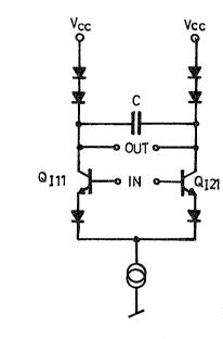
In Figure 1 there is illustrated a differential gain stage for use in the
irnplementation and control of active filters. Ths stage includes a first
amplification component Q111 and a second amplification component QI21 in
the form of two like NPN transistors with base, emitter and collector
electrodes. The base electrodes of the amplification components are connected
in counterphase directly to the differential input of the differential gain stage
so that the difference between the potential on the base electrodes increases
with increasing magnitude of the voltage VIN across the differential input.
The differential amplifier stage in Figure 1 includes a plurality of diode
components QL11' QL12' ' QLlm' QL21' QL22' QL2m' QI12' 'QI1n'
QI22~ QI2 ~ in the form of NPN-transistors of the same kind as the compo-
nents Q111 and QI21. However, the transistors which are diode components have
their base electrodes connected directly to their collector electrodes. Each
diode component thus has a forward voltage drop corresponding to the base-
emitter voltage in an amplification component.
The diode components Q-11~ QL12~ QLlm are connected in series to a first
group of m diode components. The diode components QL21, QL22, ---QL2m are
connected in series to a second group of m diode components.
The first diode component group and the first amplification component are
included together with the diode components QI12,...QI1n in a first series
circuit. The second diode component group and the second amplification
component are included together with the diode components QI22,...,QI2n in a
second series circuit.
- 3LZ~38~8~
--5--
The first and second series circuits are connected in parallel to a first current
generator Ql and to a positive or comparatively high supply voltage tlCC- The
current generator is connected to a comparatively low supply voltage or earth
so that it strives to keep the sum of the currents through the amplification
S components constant.
The differential gain stage has its differential output between the collector
electrodes of the amplification components. The first group of diode compo-
nents is thus connected between the supply voltage Vcc and one pole of the
differential output, while the other group of diode components is connected
between the supply voltage Vcc and the other pole of the differential output.
The first and second groups are thus connected in counterphase directly to the
differential output.
For an unloaded differential output, the magnitude of the current through the
first group will substantially agree with the current through the first amplifi-cation component, whereas the size of the current through the second group
will substantially agree with the current through the second amplification
component. In addition, the sum of the currents thorugh the first and second
groups will be substantially constant. Furthermore, within certain limits, therewill be substantially linear relationsship between the differential gain stage
output voltage VOUT across the differential output and the stage input voltage
VIN across the dif-ferential input. The relationship is responsive to the numberof diode components in the series circuits and can be written: n x VOUT = m x
VIN.
The effective output resistance of a differential gain stage according to Figurel varies with the current through the current generator, and also with the
magnitude of the input voltage. The output resistance variation with current is
desirable for being able to control a filter in which the differential amplifi-
cation stage is included. The output resistance variation with input voltage is
not desirable on the other hand, because the signal amplitude must then be
limited i:o low levels for reducing the harmonic distortion and for avoiding
frequency drift. The usable dynamic range of the differential gain stage would
therefore be limited.
- ~2884~36
--6--
A method of increasing the dynamic range of the differential gain stage ~Jould
be to increasc the number of diode components in each series circuit. If the
stage is to be driven by a supply voltage of only about 5 volts, the number of
diodes and amplification components in each series circuit cannot, however, be
greater than four when the diode components are connected according to Figure
1.
In Figure 2 there is illustrated a second ernbodiment of a differential gain
stage, in which certain diode components are connected in ano~her way than in
the differential gain stage according to Figure 1, whereby the total number of
diode cbmponents and usable dynamic range of the differential gain stage can
be greater.
The differential arnplifier stage according to Figure 2 includes a first amplifi-
cation component Qlll and a second amplification QI21 in the form of two like
NPN-transistors with base, emitter and collector electrodes. The base electro-
des of the amplification components are connected in counterphase directly to
the differential input of the differential gain stage.
A first group of n-l series-connected diode componen~s QIl2~..QIln forms a
first series circuit together with the first amplification component. A second
group of n-l series-connected diode components QI22,....QI2n forms a second
series circuit together with the second amplification component. The first and
second series circuits are connected in parallel to a first current genarator Ql'
which is connected to a comparatively low supply voltage, so that it strives to
keep the sum of the currents through the series circuits substantially constant.
A third group of m series-connected diode components QLll,...QLlm is
connected between a second current generator Q2 and the comparatively low
supply voltage. The collector electrode of the first amplification component is
also connected to the second current generator. One pole of the differential
output of the differential amplifier stage is also directly connected to the
second current generator.
A fourt!1 group of m series-connected diode components QL2l~.. QL2m is
connected between a third current generator Q3 and the comparatively low
1~88~
supply voltage. The collector electrode of the second amplification component
is also connected to the third current generator. The second pole of the
differential output of the differential gain stage is also directly connected tothe third current generator.
The second current generator is connected to the comparatively high supply
voltage Vcc so that for an unloaded differential input it strives to keep the sum
of the currents through the First series circuit and through the third group
constant. The third current generator is connected to the cornparatively high
supply voltage Vcc so that for an unloaded differential output it strives to keep
the sum of the currents through the second series circuit and through the fourthgroup constant. The first, second and third current generators are set for
generating substantially equally as great currents. For an unloaded differentialoutput, the size of the current through the first amplification component will
thus be substantially equal to the magnitude of the current through the fourth
group. For an unloaded differential output, the magnitude of the current
through the second ampliFication component will furthermore be substantially
equal to the magnitude of the current through the third group.
Each diode component in the first, second, third and fourth groups is a
transistor of the same type as the amplification components, but with the base
and collector electrodes connected together. The forward voltage drop across
each diode component in the first and fourth groups therefore agrees with the
base-emitter voltage o F the -first amplification component. In addition, the
Forward voltage drop across each diode component in the second and third
groups substantially agrees with the base-emitter voltage of the second
amplification component. Within certain limits, there is therefore a substan-
tially linear relationship also with the differential amplifier according to Figure
2 between the differential gain stage output voltage VOUT across the differen-
tial output and the differential gain st~ge input votlage VIN across the
differential output. The relationship is responsive to the number of diode
components in the third and fourth groups in relation to the number of diode
components in the first and second groups, and may be written: n x VOUT = m x
VIN.
~L28848f;
For maxirnum supply voltage of only aboùt 5 volts, the number of diode
components in the third and fourth group in Figure 2 can only be up to foùr At
the same time, the number of diode components in the first and the second
group can be two. Thus, for a supply voltage of 5 volts the number of diode
cornponents can be substantially more for a differential gain stage according toFigure 2 than for such a stage according to Figure 1. The usable dynamic range
of a differential amplifier according to Figure 2 can therefore be greater than
for such an amplifier according to Figure 1.
In Figure 3 there is illustrated a third embodiment of a differential amplifier
stage with more diode components and greater dynamic range than the
differential gain stage in Figure 2. The differential stage in Figure 3 includes a
first ampli-Fication component QI11 included in a first series circuit together
with a first group of diode components Ql12 al13~ a second amplification
component QI21 included in a second series circuit together with a second group
1 5 of diode components Ql21' QI23~ a third group of series-connected diode
components QL11' QL12' QL13' a fourth group of series-connected diode
po nts Q-21' Q-22' Q-23' a fifth group of Series-cQnnected diode
components Ql14' Ql15' QI16~ a sixth group of series-connected diode compo-
nents Ql24' Ql25' Ql26~ a seventh group of series-connected diode components
Q-14' QL15' Q-16' Q-17' an ei9hth group of series-connected diode compo-
L24' Q-25' Q-26' Q-27' a first~ second, third, fourth, fifth, sixth,
seventh current generator Q1' Q2~ Q3~ Q4' Q5' Q6 and Q7.
The first series circuit and the third group are connected in parallel to the
second current generator Q2. The second series circuit and the fourth group are
connected in parallel to the third current generator Q3. The fifth and sixth
group are connected in parallel to the first current generator Q1 The first
series circuit and the fifth group are connected in parallel to the fourth current
generator Q4- The second series circuit and the sixth group are connected in
parallel to the fifth current generator. The third and seventh groups are
3û connected in parallel to the sixth current generator Q6 The fourth and eighth
groups are connected in parallel to the seventh current generator Q7.
The first, second and third current generators are connected to the comparati-
vely high supply voltage Vcc, while the fourth, fifth, sixth and seventh current
128848~i
generators are connected to the comparatively low supply voltage or earth. The
current generators strive to generate equally as great currents.
The amplification components QIll and QI21 have their control electrDdes
connected in cDunterphase directly to the differential input IN of the differen-tial gain stage and their collector electrodes connected in counterphase directly
to the differential output OUT of the differential gain stage. The third and
fourth groups are connected in counterphase directly to the dif-Ferential outputalso.
The diode components are mutually alike and each comprises an amplification
component of the same type as the first and second amplification components
but with the base and collector electrodes connected together. Each diode
component therefore has a forward voltage drop responsive to the currents in
the same way as the base-emitter voltage of the amplification components.
The differential gain stage in Figure 3 functions in a similar way as those of
Figures l and 2, but has more diode components and a greater usable dynamic
range. The differential gain stages in Figure 2 and 3 do not solely have
advantages compared with the differential gain stage in Figure l. The com-
plexity of the amplification stages is greater, and they have greater stray
capacitances, which leads to poorer properties at high frequencies for filters
implemented with the aid of the differential gain stages. Transistors of the
PNP-type are required for certain of the current generators, while only
transistors of the NPN-type are required for the diode components and
amplification components. Depending on the manufacturing process, when both
PNP and NPN transistors are required in the current generators, this may cause
undesired capacitive loads in them. Such capacitive load can deteriorate the
properties at high frequencies of filters in which the differential gain stages are
included. The differential gain stage in Figure l can therefore be preferable incertain filters, in spite of everything, at least when the high frequency
properties are important.
In Figure 4 there is illustrated a first order low-pass filter implemented with
the aid of a differential gain stage according to Figure l. The low-pass filter
differs from such a differential gain stage in principle only by a capacitive
12~38486
~10-
component in the form of a capacitor C connected across the differential
output. ~rhe low-pass filter thus has a first series circuit with a first group of
two diode components, a first amplification component and a further diode
component. In addition, the low-pass filter has a second series circuit with a
second group of two diode components, a second amplification component and a
Further diode component. The series circuits are connected in parallel bet-r/eenthe comparatively high supply voltage and a current generator.
The low-pass filter in Figure 4 has substantially the same transfer function as a
-first order RC-filter. Since the output resistance of the differential gain stage
is responsive to the current through the diode components, the output reistance,and thereby the limiting frequency of the low-pass filter, can be controlled by
controlling the current through the current generator.
In Figure 5 there is illustrated a filer which attenuates low frequencies by about
6 dB compared with high frequencies. The filter in Figure 5 includes a
differential amplification stage according to i~igure l. The filter differs fromthis differential gain stage in principle only by a capacitive component C beingconnected between the series circuits on the opposite side of the amplification
components as is the differential output. The control electrodes of the
amplification components are thus connected in counterphase directly to the
Z0 filter input, while the collector electrodes of the amplification components and
groups of diode components are connected in counterphase directly to the filter
ou tpu t.
In Figure 6 there is illustrated a second order low-pass filter of the Butterworth
type. This filter includes a first low-pass filter similar to the one in Figure 4,
where the input IN constitutes the input of the entire low-pass filter. The first
low-pass filter includes a first series circuit with the diode components Dl andD2 as well as the amplification component Q Ill- The first low-pass filter also
includes a second series circuit with the diode components D3 and D4 as well as
the amplification component QI2l. The first and second series circuit in the
first low-pass filter are connected in parallel between the high supply voltage
V and a current generator Ql' Rl. A capacitive component Cl is coupled
across the output of the first low-pass filter.
1~38486
-11 -
The low-pass filter according to Figure 6 also ;ncludes a second low-pass filtersirnilar to the low-pass filter in Figure 4, the output of which constitute~ theoutput of the entire low-pass filter. The second low-pass filter includes a first
series circuit with the diode components D5 och D6 as well as as the
amplification component Q112 The second low-pass filter aslo includes a second
series circuit with the diods components 1~7 and l~iB as well as the amplification
component Q122 The first and second series circuits of the second lo~ pass
filter are connected in parallel between the high supply voltage Vcc and a
current generator Q2~ R2. A capacitive cornponent C2 i9 connected across the
output of the second low-pass filter.
The output of the first low-pass filter is connected to the input of the second
low-pass filter. In addition, two substantially alike series circults are connected
to the output of the first low-pass filter. One of these series circuits comprises
the amplification component Q113 and the diode component D9, while the
second of these series circuits comprises the amplification component QI23 and
the diode component D10. Both the last-mentioned series circuits are connected
in parallel to a current 9enerator Q3, R3. The control electrodes of the
amplification components QI13 and QI23 are connected in counterphase directly
to the output of the second low pass filter.
Z0 In the low-pass filter according to Flgure 6, the diode components D1 to and
including D10 are commonly alike, which also appliPs to the amplification
components, Ql11 up to and including Q~23. The current generators Q1~ R1 and
Q3, R3 are also alike, while the current generator Q2' R2 differs from the othertwo. The low-pass filter includes means Q4, R4, Q5 for synchronous control of
the currents through the current generators, these and the control means being
dimensioned such that the currents through Q1 and Q3 will be equally as great,
while the current through Q2 will be twice as great. The magnitude of the
currents through the current generators is controlled with the aid of a current
ICTL supplied to the control means.
3~ In Figures 7a and 7b there is illustrated a simplified block diagram over
principles known per se for controlling filters with the aid of an oscillator and a
- frequency-locked loop FLL and a phase-locked loop PLL, respectively. Since
these controlling prinicples are well known they are not described here. By their
~ ~3848~
-12 -
use, a current ICTL can be generated for a control means in a filter acc~3rdin~
to Figure 6, for example.
An oscillator is illustrated in Figure 8, for use in controlling filters according to
the invention, such that the filters can be controlled according to a known
principle illustrated in Figure 7.
The oscillator according to Figure 8 includes First, second and third low-pass
filters of principly the same kind as illustrated in Figure 4. The first of these
low-pass filters includes diode components Dl, D2, D3, D4, the capacitive
component C1, amplification components Qll' Q12 and the current generator
Ql' R1. The second of these low-pass filters includes the diode components D5,
D6, D7, DB, the capacitive component C2, ths amplification components Q21~
- and Q22 and the current generator Q2' R2 The third of the low-pass filters
includes the diode components D9,DlO,Dll,D12, the capactive component C3,
the amplification components Q31 and Q34 and the current generator Q3,R3.
The amplification components Qll-Q32 of the low-pass filters are alike. The
diode components Dl-D12 are also alike, and each diode component comprises
an amplification component of the same kind as Qll-Q32 but with the base and
collector electrodes connected together. The current generators Q1~ R1; Q2,R2
and Q3,R3 are also commonly alike. The oscillator has a control means Q4, R4,
Q5 for synchronous control of the current generators. Control takes place with
the aid of a current ICTL supplied to the control means.
In the oscillator of Figure 8, the first low-pass filter output is connected to the
input of the second low-pass filter. The output of the second iow-pass filter isconnected to the input of the third low-pass filter. The output of the third low-
pass filter is connected to the first low-pass filter input.
Since the oscillator of Figure 4 principly comprises three low-pass Filters
implemented with the aid of the same type of differential gain stage as the
filters for which the oscillator is implemented for use together with, special
advantages are achieved with regard to temperature stability, ageing, manufac-
turing tolerances etc.
- ~ ~X88~6
In Figures 4, 5, 6 and 8 there have solely been illustrated implementation and
control with the aid of differential gain stages - of the more simple type
illustrated in Figure l. Of course, differential gain stages according to Figure 2
or 3 can be used for the implementation and control of filters in a similar ~Jay.
Pdthough the differential gain stage in Figure l and the filters in Figures 4, 5and 6 only include amplification components in the form of NPN transistors
with base, emitter and collector electrodes, this is not absolutely necessary, of
course. Within the scope of the invention it is naturally conceiYable to use
somewhat different amplification components of a kind such that the desired
relationship bewtween the forward voltage drop of the diode components and
the voltage drops of the amplification components can be obtained.