Note: Descriptions are shown in the official language in which they were submitted.
~L2~S23
DATABASE ACCESS MACHINE FOR FACTORY AUTOMATION
Backgrsund of the Invention
1. Field of the Invention
- The field of the invention is computer equipment for
linking a plurality of machine or process controllers in a
factory automation network.
2. Description of the BacXground Art
In factory automation, more complex functions could be
performed and coordinated if the programmable or computerized
machines presently used to control mechanical equipment
could be connected in a network with each other and with
higher level supervisory computers. A network would allow
the "reconfiguring" of the assembly line by communicating
new programs to the programmmable systems from a central
computer. The network would also provide numerous monitor-
ing and report functions at designated locations and these
would provide managers with information to further improve
efficiency of manufacturing operations.
Many programmable tools, instruments and control systems
are now installed in industry, however, many of these program-
mable machines cannot communicate with each other. It has
been estimated that to establish such communication through
custom hardware and software interfaces may account for up
to 50 percent of the cost of factory automation.
In anticipation of acquiring a large amount of program-
mable equipment to automate its factories, certain large
manufacturers have established MAP (Manufacturing Automation
Protocol). MAP is a seven-layer communications specification
for interconnection of general purpose mainframe computer
equipment to specialized computer controllers that control
~k
~, ~ ' ' - ' .
', ~ '' ' , ' " ' ~
:~ j
~2~3~1523
individual machines or processes. The MAP standard is not
complete at all seven of its layers and is still in the
process of development. The MAP standard i5 also being
implemented in phases as equipment has not been available to
meet all of the MA~ specifications, and new eguipme~t i8
being designed to provide the MAP-networking capability.
Demonstrations of early phase ~AP networkæ have pointed
to possible problems that have not a~ yet been addressed or
solved. One problem has been the time involved in download-
ing programs and data from supervisory computers to stationson the factory floor. Even if computers are able communicate,
communication networks can develop bottlenecks where too many
messàges are required to accomplish a certain tasX, where
redundant data is being communicat~d or where too many
protocol translations are required. Another problem has
been the need for central computers to recompile entire
application programs to implement simple changes in data
tables or in the arrangement of discrete devices on equipment
being controlled by station-level controllers.
When an application program is written on a central
computer, items of data or variables stored at station level
are represented by certain label rather than specific
addresses or locations in memory where they will be found.
When the application program is compiled, the items o data
~5 in the program are assigned addresses in the memory of the
central computer.
At the stations some da~a variables are related to the
physical connection o device~ on the controlled machine.
When an additional device, such as a photoelectric sensor,
is connected the programmable controller, a new data item is
created in the memory of the programmable controller. Other
-2
'
. .
~ Z8~35Z3
01 new data items such as timing variables may be created in the
02 memory of the programmable controller without connecting
03 additional devices to the controller.
04 In one MAP demonstration, the incorporation of the new
05 data item or variable at the station level required a
06 recompilation of application programs and data files at the level
07 of the central computer. In this instance recompilation was
08 required to relate the address or location of the new variable at
09 the station level to an address or location in the data files of
the central computer.
11 Although standardization of communication network
12 standards is an important development, reaching the goals of
13 factory automation will also reyuire innovative solutions such as
14 those offered by the present invention.
SummarY of the Invention
16 An embodiment of the invention is an access computer
17 which is a first of a plurality of access machine computers for
18 connection in a factory automation cell that includes a cell
19 controlling computer and a plurality of station-level computers
located at a corresponding plurality of stations. The plurality
21 of station-level computers include at least one station-level
22 computer controlling an industrial machine in real time. The
23 first access machine computer is comprised of an access machine
24 module outside the cell controlling computer for communicating
upstream within the factory automation cell to the cell
26 controlling computer and for communicating downstream within the
27 factory automation cell to a plurality of station-level
2~ computers. The access machine module includes database apparatus
29 for storing at least a portion of a database associated with the
first access machine computer, the database including data
31 items. The cell controlling computer accesses the data items on
32 a basis that is independent of the addresses which are assigned
33 to the data items at the stations for reference by respective
34 station-level computers. The access machine module also includes
first network communication apparatus coupled to the database
36 apparatus for communicating the data items associated with the
37 first access machine computer through a first network
38 communication link to and from the cell controlling computer via
39 - 3 -
,~
'~' ' ' ' ' ' ,,~' ' "''' ~
- .
:
'
:. , ,
~2~3523
01 messages in which the data items are stored in and retrieved from
02 the database independent of the addresses which are assigned at
03 the stations at which the data items are monitored or controlled.
04 The access machine module includes second network communication
05 apparatus for communicating the data items through a second
06 network communication link to and from the station-level computers
07 via messages which include station-related blocks of information
08 that are related to addresses of the stations of the respective
09 station-level computers. The addess machine module also includes
database interface apparatus interfacing the database apparatus to
11 the second network communication apparatus for translating the
12 data items between the station-related blocks of information and
13 the station-independent organization of the database.
14 Another embodiment of the invention is an access
machine computer which is a first of a plurality of access
16 machine computers for connection in a factory automation cell
17 that includes a cell controlling computer and a plurality of
18 station-level computers located at respective stationsl the
l9 plurality of station-level computers including at least one
computer controlling an industrial machine in real time. The
21 first access machine computer is comprised of a data access link
22 processor module including database apparatus for storing at
23 least a portion of a database associated with the first access
24 machine computer. The database includes data items which are
associated with stations of respective station-~evel computers
26 during communication to and from the stations. ~he cell
27 controlling computer accesses the data items on a basis that is
28 independent of the addresses which are assigned to the data items
29 at the stations for reference by respective station-level
~30 computers. First network communication apparatus is coupled to
31 the database apparatus for communicating the data items associated
32 with the first access machine computer through the first network
33 communication link to and from the cell controlling computer via
34 messages in which the data items are stored in and retrieved from
the database independent of the addresses which are assigned at
36 the stations at which the data items are monitored or controlled.
37 Second network communication apparatus communicates the data items
38 - 3a -
: ~ , .
. . ~ - , .
'12~ 3
01 through the second network communlcation link to and from the
02 statlon-level computers via messages which include
03 station-related blocks of informatlon that are related by station
04 to the respective station-level computers. Database inter~ace
05 apparatus interfaces the database apparatus to the second network
06 communication apparatus for translating the data items between
07 the station-related blocks of information and the
08 station-independent organization of the database. The first
09 access machine computer further comprises a communication link
interface module including third communication apparatus for
11 communicating the messages with station-related blocks of
12 information associated with the respective station-level
13 computers through a second communication link to and from the
14 station-level computers, and apparatus for conveying the messages
with station-related blocks of information associated with the
16 respective station-level computers between the data access
17 processor module and the communication link interface module.
18 Another embodiment of the invention is an access
19 machine which is a first of a plurality of access machines for
2~ connection in a factory automation cell that includes a eell
21 controlling computer and a plurality of station-level computers
22 located at a eorresponding plurality of stations. The plurality
23 of station-level eomputers inelude at least one station-level
24 computer eontrolling an industrial maehine in real time. The
first aecess machine is comprised of an access maehine module
26 outside the cell controlling computer for communicating upstream
27 within the factory automation cell to the cell controlling
28 computer and for eommunieating downstream within the factory
29 automation cell to a plurality of station-level computers. The
access machine module includes database apparatus for storing a
31 database in which the data items are associated with respective
32 station-level computers. The cell controlling computer accesses
33 the data items on a basis that is independent of the addresses
34 which are assigned to the data items for reference by the
respective station-level computers. First network communication
36 apparatus is coupled to the database apparatus for receiving a
37 coniguration message associated with the first access machine
38 - 3b -
.' ' ' ' ' ' ' ":" '~ ' ' .,' ' ' ' :
' ' . ' , ' ' , '~ ' ' : : '
'
'~ '.................. '
.
~l~8~S~3
01 through a EiLst netwoLk communication link from the cell
02 controlling computer, wherein the configuration message includes a
03 new data item to be added to the database. Second network
04 communication appaLatus communicates data items through a second
05 network communication link to and from the station-level computers
06 via messages which include station-related blocks of information
07 that are related to addresses of the stations of the respective
08 station-level computers. Database interface apparatus inteLfaces
09 the database apparatus to the second network communication
apparatus, the database interface apparatus including linkages
11 between the station-related blocks oE information and the
12 station-independent organization oE the database. Database
13 on-line configuration apparatus is responsive to receipt of the
14 configuration message through the first network communication link
and stores the new data item in the database apparatus and
16 establishes a corresponding linkage in the database interface
17 apparatus between the station-related blocks of information and
18 the station-independent organization of the database.
19 The access machine could be imagined as a huge set of
pigeonho~es such as those used in an old post office.
21 Station-level devices insert and retrieve information (data,
22 messages, graphic images) from one side of the pineonholes on a
23 schedule determined by the needs of the control devices. The
24 cell controlling computer inserts and retrieves information from
the other side of the pigeonholes on a different schedule
26 determined by the needs of the human interface and higher level
27 computers connected through the cell controlling computer. Each
28 pigeonhole is identified by a unique name or tag.
29 Because the access machine is a computer that is
separate from the cell controlling computer, it provides
31 distributed processing. The cell controlling computer handles
32 communciation with the user through a work station having a
33 video display, a keyboard and a mouse, while the access machine
34 handles data collection from the remote stations. The cell
controlling computer and the access machine communicate with
36 each other when necessary, but generally the access machine
37 relieves the cell controlling computer of the burden of
38 - 4 -
12~ 3
real-time data collection activities. The cell controlling
computer can therefore concentrate on .its user interface
functions.
The invention also enablss the cell controlling computer
to add or delete items from the database while the access
machine remains "on-line" and in control of machine control-
ling computers. This is referred to as "on-line reconfigura-
tion".
The invention removes any need to recompile application
programs or to reorgani~e large amounts of data in the cell
controlling computer when simple changes are made to ~he
arrangement of equipment at the stations. The invention
also provides the basis for avoiding similar problems in
higher level computers supervising the operati~n of the cell
controlling computers.
Other objects and advantages besides those discussed
above shall be apparent to those skilled in the art from the
description of a preferred embodiment of the invention which
follows. In the description, reference is made to the
accompanying drawings, which form a part hereof, and which
illlustrate a~ example of the invention. Such example, however,
is not exhaustive of the various embodiments of the invention,
and therefore reference is made to the claims which follow
the description for determining the scope of the invention.
.
Brief Description of the Drawings
Fig. l is a data flow diagram showinq the propagation
of data in a control system provided by the background art;
Fig. 2 is a hardware-to-memory map schematic diagram of
a programmable controller of a type Xnown in the art;
. ` . .
' . . .
.
~ .
~ ~85~3 --
Fig. 3 is a block diagram showing the management of
data items in a factory cell automation system that incorpo
rates an access machine of the present invention;
Fig. 4a shows the screen of the video display of Fig. 3
as a new data itam is being entered into the database of the
access machine of Fig. 3;
Fig. 4b shows the screen o~ the video display of Fig. 3
as a new station record is being entered into the database
of the access machine of Fig. 3;
Fig. 5 is a map diagram showing the relationship of
certain records in the database maintained by the cell
controlling computer and the access machine of Fig. 3;
Fig. 6 is a map diagram showing the organi~ation of
data items in a database residing in the access machine of
Fig. 3;
Fig. 7 is a data flow diagram showing the communication
of one type of database-related information in a system that
incorporates the access machine of Fig. 3;
Fig. 8 is a data flow diagram showing the communication
of another type of database-related in~ormation in a system
that incorporates the access machine of Fig. 3;
Figs. 9-15 are maps of tne database-related information
contained in messages communicated between the cell control-
ling computer and the access machine in Figs. 7 and 8;
Fig. 16 is a hardware-firmware schematic showing the
architecture of the access machine of Fig. 3;
Figs. 17 and 18 are block diagrams illustrating the
operation of data collection software in the access machine
of Fig. 3;
; 30 Fig. 19 is a schematic diagram of a processor board in
the data access link processor module seen in Fig. 16;
.
-6-
~'
-
~'':' ' . , ', "' :
:,
~2~il5~3
Fig. 20 is a schematic diagram of a memory board in the
data access link processor module seen in Fig. 16;
Fig. 21 is a schemati~ diagram of the circuitry in an
access machine processor module seen in Fig. 16; and
5Fig. 22 is a schematic diagram of the circuitry in a
local area network inter:Eace moduls seen in Fig. 16.
Detailed Description of the Preferred Em'oodiment
Figs. 1 and 2 show a system representing the art prior
to the invention. A plurality of ~tation-level devices such
as a robot controller 10 at Station 1 and a programmable
controller ll at Station 2 are connected via a irst local
network 12 to a gateway machine 13. The gateway machine 13
in turn is connected via a second network 14 to a supervisory
computer 15 which may be of the mainframe or minicomputer
class. The second network 14 conforms to the layers 1-3 of
the MAP standard and in particul~r provides a token-passing
broadband network conforming to IEEE Std. 802.4.
The supervisory computar 15 executes a number of appli-
cation programs 16 which utilize a hardware and software
communication interface 17 to send and receive message~ lB
over the second network 14. The data in these messages is
organized as a series of bytes according to a protocol
meeting the MAP standard. As an example, it shall be assum-
ed that four words of data are of particular interest. In
the application programs these will assigned labels of
MOTOR, SWITCH, ACCUM l and PRESET l. These four words of
data correspond to four items of data stored in the memory
of the programmable controller ll at Station 2.
There are two basic issues in handling the four words
of data labeled MOTOR, SWITCH, ACCUM_1 and PRESET_1. The
~ ` ' ` ` ' ',
.
~2~38523
first issue is how to organize and store the data in the
memory of the supervisory computer 15 in relation to its
location in the programmahle controller 11 at Stat~ion 2.
The second issue is how to organize the data for communica-
tion between the supervisory computer 15 and the programmablecontroller 11.
The labels are assigned to the four items of data when
an application program 16 is written in source code. When
the application program 16 is compiled to object code the
data variables in the program 16 are assigned addresses in
the memory of the supervisory computer 15 such as 10516 -
10519 (hex) based on the set of addresses available to the
CPU within the supervisory computer 15. When this data is
communicated to the programmable controller 11 it is organ-
ized in a message 18 with a station address. The stationaddress is dstected and compared by the stations to determine
that a message is being sent to it. When the programmable
controller 11 communicates the data in the other direction --
to the ~upervisory computer 15 -- th~ programmable controller
11 Includes an address for the supervisory computsr 15 in
the message.
Typically the gateway machine 13 is "initialized"
during startup operations to recognize the addresses o~ the
supervisory devices and station-level devices with which it
must communicate. The gateway machine 13 may store message
data for the respective stations in assigned areas of its
memory while it is performing protocol translation and other
message handling functions. It may store message data
moving downstream to the stations in one set of memory areas
and message data moving upstream to the supervisory computer
15 in another set of memory areas. For messages 1~ moving
'" ' ~ , ,. . :
;..
.
. ~ . . .
.
~l2~385Z3
downstream, the station addresses are carried through to
messages 18 on the local network 12. For messages moving
upstream an address for ths supervisory computer lS i8
usually included in the messages returned through the MAP
network 14.
Besides a station level addre s, each item of data has
a particular address where it is located within the station.
This address may be expressed as a higher-level user program
address or as a lower-level machine address. The user
proyramming address is expressed in the octal numbering
system which has been devaloped for programmable controllers.
The addresses "010", "030", l'llO" and "130" are the user
programming addresses for the four items of data to be
communicated to and from Station 2. These user programming
addresses are translated within the programmable controller
11 to a set of machine-level addresses used by the microelec-
tronic CPU within the programmable controller 11. For
purposes of this discussion, reference will be made to the
user programming addresses.
In the prior art exemplified in Eig. 1, som~ form of
data addressing or identification is provided for each item
of data in addition to the station-level address. A messaga
is formed with station-level and data-level addresses and is
sent from the supervisory computer 15 to the programmable
controller 11, with any necessary protocol translations
being made along the way. This would reguire considerable
time for the values of data items in the memory of the
supervisory computer lS to be sent downstream to the program-
mable controller 11 and for the values of data itams in the
memory of the programmable controller 11 to be sent upstream
to the memory of the supervisory computer 15. If the data
. . ~ ~.................. .
.~ . . .
: ~ :
' ' '' ,, ~ , .
:' :
:. :
12~35~3
items were located at four different stations, tha number of
messages and comunication time would be multiplied by a
factor of four.
Fig. 2 illustrates the nature of the particular data
items in this example. The programmable controller 11 is
connected to control a conveyor motor 27 in delayed response
to signals from a limit switch 23. ~he delay has been
incorporated solely for the purposes of illustrating the
different types o~ data in the controller 11, and this
example should not be taken as a suggested program for real-
life operation of such equipment.
~ he programmable controller 11 includes a processor 20
with a main memory 21 for storing the data items. The proces-
sor 20 is connected through an input module 22 to the limit
switch 23. The limit switch 23 contacts are normally closed.
These contacts will be opened when the switch arm is contacted
by a package 25 moving along the conveyor 24. This will
change the logic state of a signal that is sent to the
processor 20 through the input module 22. The procassor 20
is also connected through an output module 26 to a motor 27
for moving the conveyor 24. The processor 20 can generate a
signal to start the motor 27, and in response to the opaning
of the limit switch contacts, and after a programmed delay,
it will remove the signal to stop the motor 27 and the -
conveyor 24.
To accomplish this operation, a status bit of data that
represents the state of the limit switch 23 is stored in an
input image table 29 in the memory 21 of the programmable
controller 11. The status bit for the limit switch 23 i5
stored at bit "10" (octal) in the high byte of a 16-bit data
word at address "110". A status bit o~ data that represents
--10-
. ~' '
- . :: . . - :
.
:
.. . ' ~ ':
: . : - ''
~28~35~3
the "on" or "of" state of the motor 27 is stored in an
output image table 28 of the memory 21. The status bit for
the motor 27 is stored as bit "00" in the low byte of a
16-bit data word at address "OlO" (octal). The processor 20
executes a control program 30, which is represented in the
symbolic language that has ~een developed in the art of
programmable controllers, to checX the input status of the
limit switch 23 and to set the output status of the motor 27
according to the logic of the program 30.
The execution of the control program is sometimes
referred to as the control program "scan". The processor 20
also periodically executes an "I/0 scan" to read th~ status
of the limit switch 23 and to control the operating state of
the motor 27. The I/0 scan is executed many times per
second so that the response of the programmable controller
11 to actual operating conditions on the conveyor 24 appears
instantaneous to the naked eye.
Status ~its representing physical devices such as the
limit switch 23 and the motor 27 are one type of data used
by a programmable controller 11. Another type o data
exists in the memory 21 of the programmable controller 11,
but does not correspond to an external physical device.
This type of data is exemplefied by the preset and accumulat-
ed values for timers and counters.
As seen in the memory map of Fig. 2, the output image
table 28 is followed by an area 31 for storing the accumulat-
`ed values for timers and counters that begins as address
"030" (octal) in the memory 21. The accumulated value
ACCUM_1 is stored at word "030" as three binary-coded decimal
(BC~) digits with four control bits as the four highest
order bits (bits "17" - "14"). Preset values for the
-11--
-, . ., ~ .
' ~
,
: ' ~' ' ,~. '
" ~ '
~2~3~35~3
timers and counters are stored in an area 32 following the
input image table 29. The preset value PRESET 1 i8 stored
at word "130" as three binary-coded decimal (BCD) digits
with four control bits as the four highest order bits (bits
"17" - "14").
With this background, the function of the timer and
- counter data can be explained with reference to the example
control program, which is presented in a ladder diagram with
two rungs, Rung A and Rung B. I all of the conditions in a
rung are "true", then an output action for the the rung will
be executed. The first and only conditional instruction in
Rung A is an XIO instruction for the limit switch 23. The
XIO instruction is interpreted as "examine the limit switch
status bit at bit "00" of memory location "OlO" to see if
the limit switch contacts are opened." If 50, the condition
is satisfied, and the output action represented by the next
instruction is executed. The next instruction in Rung A is
a TIMER ON DELAY ~TON) instruction.
The TIMER ON DELAY (TON) instruction is represented in
the ladder diagram program as follows. The "030" above the
symbol "(TON)" means that the accumulated value for this
program timer is stored at address "030" ~octal) in the
memory 21. The number "1.0" below the symbol "(TON~" means
that the timer is operated at 1.0 second time base. Each
time the timer runs for a second the accumulated count is
advanced by one. The legend "PR 010" means that the preset
number is a decimal "lO", and that after 10 counts the
accumulated value will equal the preset value to indicate
that the timer has timed out. When this occurs bit "15"
(octal) in word 030 will be set.
,' . , ' ' ' ~ . :
'. ., ~ '~ , ' . :
.
~Z~38S~;~
To summarize Rung A of the ladder dlagram program, if
the limit switch contacts are open for 10 seconds elapsed
time, set bit "15" in data word "030" to signal completion
o~ a timing cycle. In Rung E~, a second XIO instruction is
S programmed with an "energi~e output" (OTE) instruction.
When this rung is true, this instruction will maintain the
output status bit "00" of word "010" in a set state to
energize the motor 27. When the XI0 instruction becomes
false (signalling the timer has timed out) Runy B is inter-
rupted and the motor status bit is reset to deenergize themotor 27. Of course, other logic instructions would be
added to this example to be sure that the motor did not run
continuously.
As seen from the above example, the status bits in the
input and output image tables 28,29 are related to physical
devices on the controlled machine. The locations in tha
programmable controller memory 21 correspond to terminals on
the input and output modules 22, 26 so that status data can
be transmitted between the processor 20 and the physical
devices during the I/O scan. The I/O address of the limit
switch 23 and the motor 27 and the address of their status
bits in memory depends upon which terminals on the input
module 22 and output module 26 are wired to the limit switch
23 and to the motor 27. When an additional device, such as
a photoelectric sensor, is connected to a terminal on the
programmable controller 11, a new data item is created in
the memory of the programmable controller 11.
The preset and accumulated values for timers are program
data variables rather than "status" data variables correspond-
ing to the the physical connection of control devices on the
-13-
.: - ' ' ' . . ' . :
.. -. : -
. ' ' ' , . .
:
35~3
conveyor 24. Nevertherless, the programming of such values
creates new data variables with an address in the memory of
the station level device.
Returning to Fig. 1, it can now be appreciated thak new
data variables can be created at Station 2 in several ways.
An application program 16 m:ight be written for the supervi-
sory computer 15 to monitor execution of the user control
program at Station 2 and depending upon ths status of certain
variables at Station 2, it might signal the robot controller
at Station 1 to begin execution o~ a user control,program.
If, however, a new variable is added to the variables MOTOR,
SWITC~, ACCUM_1 and PRESET_l, there had not been an easy way
to alter the application program 16 without recompiling the
application program 16 to assign a new memory location to
hold the value of the new variable.
Besides the recompilation problem, the system in Fig. 1
causes a great number of messages to be communicated, where
there are many application programs 16 and many more stations
than shown. The large number of communication messages
lengthens the system response time in the real-time factory
environment.
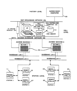
In Fig. 3, there are two levels or tiers above the
station level as compared with one higher level in Figs. 1
and 2. A cell controlling computer 40 is located at a cell
level that is one level above the station level. The cell
controlling computer 40 is connected ~or communication with
a supervisory computer 56 at the factory level through an
I/O bridge module 53. The supervisory computer 56 may be of
the mainframe or minicomputer class.
The cell controlling computer 40 comprises a work
station ~1, a power supply unit 42, a cell processor and
. - . ~ - .
.
~ ` ' ' ' ' : ' ' :'
- -, . ' : . . :
~ ' - ~,
~l~8~S~3
memory unit 43 and a hard disk memory unit 4~. These units
41-44 are housed in separate enclosures. The control center
or brain of the cell computer system is the cell processor
and memory unit 43. This unit 43 contains processor and
memory modules. Within the processor module ia a microelec-
tronic CPU from the 68000 Series of CPU's manu~Acturad by
Motorola, Inc. of Phoenix, Arizona, and Austin, Texas. The
memory modules contain four megabytes ~8 Mb) of random
access memory (RAM) storage capacity. The work station 41
and the hard disk memory unit 44 are peripheral~ connected
to the cell processor and memory unit 43. The power supply
unit 42 provides power to the other units in ~he system.
The work station 41 includes a color video display 45 and a
separate Xeyboard 46 and mouse (not shown). The hard disk
memory unit 44 provides sevety-one megabytes (71 Mb) of
storage capacity and is useful for saving application programs,
databases and other data files and reloading these items
into the 8-meqabyte RAM on startup.
The cell controlling computer 40 is compatible with the
Series 5500 Computer Systems available from Massachusetts
Computer Corporation, Westford, Massachusetts. It runs
under the UNIX~operating system available rom AT&T Bell
Laboratories, Short Hills, New Jersey.
The cell controlling computer 40 is connected through a
data access baseband network 49 to two access machines o~
the present invention, referred to as ACCESS ~CHINE 1 and
ACCESS MACHINE 2. The baseband network 49 is a carrier
sense multiple access/collision detection (CSMA/C~) type as
specified in IEEE Std. 802.3.
- Trade Mark
-15-
- ~ ' - ' "
' " ' . ' ' .
~: . ' ' . .
. . .
~'~8~3523
The IEEE 802.3 specification is a development of the
Ethernet Version 1.0 specification, published by DEC, lntel
and Xerox on September 30, 1980. The IESE 802.3 speciica-
tion has three additional features:
~EARTBEAT, which requires the transceiver to send
back a "heartbeat" signal to the controller immedi-
ately aftPr the successful transmission of a pacXet;
JABBER, a transceiver function which requires that
the transceiver stop transmission .i~ the controller
attempts to transmit a packet of much greater
length than allowed by the speciication (12,144
bits plus preamble); and
~ALFSTEP SIGNALLING which allows the transceiver
to be used with controllers having AC-coupled
input/output circuits.
The data access baseboard network (4~) consists of the
following functional blocks:
1. A passive broadcast medium (coaxial cable),
2. A transceiver (transmitter-receiver for the coaxial
cable),
3. Connectors for connecting transceivers to a coaxial
cable segment and for connecting coaxial cable sections
together,
4. A channel clock,
5. A channel data ehcoder and decoder,
6. A preamble generator and remover, and
7. Carrier and collision detect circuits.
The coaxial medium is the common element in the entire
network. A transceiver is required for each station connected
to the medium.
-16-
.
':
, .
~2~3~3S~3
The data access baseboard network 49 is connected
through an I/O bridge module 53 to a broadband network 55
conforming to the MAP protocol as specified to date and
conforming to IEEE Std. 802.4 for a token-passing bus network.
Through the MAP network 55, the cell controlling computer is
connected to the factory level supervisory computer 56.
A system database 62 is stored in the cell controlling
computer 40 and would be substantially duplicated in ACCESS
MACHINE 1, if it were the only access machine in the system.
The system database 62 can be expanded through ACCESS MACHINE 2,
so that PA~T 1 of the system database 62 is stored ln ACCESS
MACHINE 1 and PART 2 of the system database 62 is stored in
ACCESS MAC~INE 2. The database 62 serves as an interface
between a plurality of station-level devices l0, 11 and
15 57-60 and the cell controlling computer 40.
The programmable controller 11 at Station 2 is connected
to ACCESS MAC8INE 1 through one of two ba~eband local area
networks (LAN's~, referred to as BASE~AND LAN 1 and BASEBAND
LAN 2 in the drawing. Information, including the four items
of data discussed in relation to Figs. 1 and 2, is communi-
cated through BASEB~ND LAN 2 between the programmable control-
ler 11 at Station 2 and ACCESS MACHINE 1, where it is reor-
ganized according to the structure of the database 62. The
preferred networks are offered under the trade designation
Data Highway by Allen-Bradley Company, Inc. of Highland
Heights, Ohio. ~or a description of the construction and
operation of these networks, reference is made to Grudowski
et al., U. S. Pat. No. 4,319,338, issued March 9,1982, and
the co~mercial literature available from Allen-Bradley
Compan~, Inc.
-17-
, ' , ' ''. : ':
' , : ' ' :
~'- ,:
.,: . ` ' - .
. ''
~L2~3~35~3
During startup operations, the database 62 is downloaded
from the cell controlling computer 40 to ACCESS MACHINE 1.
As operations continue, messages are transmitted over the
data access baseband network 49. As will be explained in
more detail later herein, the character of these messages is
substantially different than the messages discussed earlier
in relation to Figs. l and 2 and substantially different
than the character of the messages transmitted over BASEBAND
LAN 2 to and from the programmable controller 57. The
messages transmitted over the data access baseband network
49 are organized as database operations messages.
As seen in Fig. 3, a second access machine, ACCESS
MACHINE 2, can also be connected to the data acces~ baseband
network ~9. PA~T 2 of the database 62 i 8 downloaded to
AC OE SS MAC~INE 2 through the bas_band network 49. This part
of the database 62 serves as an interface to station level
devices 58-60 which communicate with ACCESS MACHINE 2 through
BASEBAND LAN 4. Still other station-level devices can be
interfaced to the database 62 and ACCESS MACHINE 2 through
BASEBAND LAN 3~
As explained in relation to Figs. 1 and 2, there is a
problem in the art of multiple-tier computer systems in
relating the addresses of data items in a higher level
computer to the addresses of the same data items in a station-
level device. The transportation and translation of messagesfrom the highest level to the lowest level o the system
slows system response time.
~ he invention provides a database machine as an inter-
face between the station level devices and higher levels of
the system. The database is constructed to serve the entire
system with each item of data in the computer system of Eig.
-18-
- . , . . :,
- . , ,
. . .
.
~288S~3
3 bsing assigned a "tag", or global identifier. The tag
provides an identifier of the type used in database opera-
tions and also serves as a convenient cross~reference for
relating the item of data to various address locations in
S various machines in the computer system.
Generally, a database is or~anized with dif~erent types
of data files. Data files are the large~t groupings of
infor~ation in the database. A database management program
organizes the link~ and relationships between separately
identified files. Within a file ara a plurality of records
and within each record are a number of fields which are the
headings for items of information in ths record. One of the
fields is usually designated as an identifier, and the
identifier field is included in each record that i8 to be
lS linXed to the identifier. In the present computer system,
the identifiers are the tag names.
Some particular records used by the database 62 are
illustrated in Eig. 4a. Information is entered into the
system through the work station keyboard 46 and reviewed on
the video di~play 45. Fig. 4a shows the record creation
form as it would be viewed on the video display 45.
One by one the field or "atom" labels are highlighted
on the screen. The name of the highlighted fieîd ("TYPE")
appears next to a cursor field 63 at the bottom of the
screen ~S, where letters are typed in as a cursor 64 move3
from left to right to indicate the location of the next
letter. Also shown in the cursor field 63 between the
symbols "< >" is the number of characters allowed in the
field. When the information has been entered and verified
to the satisfaction of the user, the "f3 COMMIT" command is
entered to add the record to the files in the database 62.
-19-
.
- . :
.
.
8~X3
The labels "fl NEXT TAG .... f4 DELETE" in Fig. 4a signify
commands that can be entered by operating keys "f" and "1"
or by touching the screen where the command is displayed.
A record is created for each data item such as the four
data items in the programma~le controller 11 described in
Figs. 1 and 2. As æeen in Eig. 4a, the fields are grouped
in four sections which include a general section, a parameter
section, a description section and an alarm parameter section.
Within the general section, for example, there are fields
for tag name, data type, a textual description and "in
service" status. The "Tag Name" assigned to the MOTOR data
item from Figs. 1 and 2 is "MOTOR". Some o the various
types of data items for the "Type" field are BIT, NUMBER,
TEXT. A logical bit in the memory of the programmable
controller 11, such as the MOTOR status bit would be of the
BIT data type. An accumulated value for a timer such as the
ACCUM 1 value would be a NUMBER data type. Data that is
transmitted in ASCII format to be displayed on the screen of
the CRT as an English-language phrase would be of the TEXT
data type.
A record is also generated for each station in the
system and the form for creating such a record is seen in
Fig. 4b. The station also receives a tag name, which in
this example is CONVEYOR. This tag is identified as a
station tag by the term STATION that is entered in the
"Type" field. Other fields for the station record are
grouped within a parameter section, a description section
and an alarm parameter section. It should be noticed that
the station tag is also entered as one of the fields in the
parameters section of the form in Fig. 4a for creating data
item records.
-20-
.
-
.. : . . .
.
., ~ ' ' ~ ' ' . ~
~8S~3
Fig. 5 shows how the station identifier i9 used torelate the station record to all of the records of data
items at a particular station. A tag name such as MOTOR has
been entered to identify a data item record corresponding to
the MOTOR status bit in the programmable controller 11 at
Station 2. The station identifier l'CONVEYOR" ha~ been
entered to identify the location of the data item. Four
records can be created for the data items MOTOR, ACCUM 1,
SWITCH and PRESET_l shown in Figs. 1 and 2, and all cross-
referenced to the station record for the "CONVEYOR" station.In this way all data item records can be related to a particu-
lar station and to the information in the station record
without repeating the station in~ormation in each data ltem
record.
Fig. 5 also shows how the information entered in the
forms of Figs. 4a and ~b is stored in records in the cell
controlling computer 40 and in the access machines. ~hese
records contain a number of fields, which are also referred
to as "atoms". The following is a list, in alphabetical
order, with short descriptions, of the some of the atoms
commonly found in the various records which shall be discus-
sed later.
CSTATE Atom - this atom is a read-only atom which
indicates certain status information about a data item, such
as whether the data item has been updated the first time,
whether the data item is being updated at the desired rate,
and whether the data is valid.
CVADDR Atom - this atom represents the remote station
taDle address of the CVALUE (command value) ato~.
CVALUE Atom - this atom represents a command value that.
can be written to a data item.
-21-
- : .
~:
: '
~ 2a !35~3
INSERV Atom - this atom is bit-oriented, two-state atom
that signals whether the data item is operational.
RATE Atom - this atom is a code representing a scan
class category for updating the data item.
RMTFMT Atom - this atom indicates the numbering system
in which the data is repres~ented, such as 3-digit BCD, 16
bit unsigned binary, single bit binary, ASCII code or one o
the representations used for timers and counteræ in program-
mable controller 11.
RSTATN Atom - this atom is a tag name o tha network
station from which the data item is to be collected.
TAG Atom - this is the data item global identifier.
TYPE Atom - this atom is a description of the type of
data identified by the TAG atom. This description may be at
the data item level such as the types BIT, TIMER or TEXT, or
the description may be at a system level such as a STATION.
VADDRS Atom - this is a station data table addres for
the VALUE atom.
VALUE Atom - this atom is either a default value or the
collected value ~or a data item
As seen in Eig. 5, each data item record in the cell
controlling computer 40 includes display parameters for
viewing the record on the video display of the work station
41. These display parameters include the fields seen in tha
"Description" section of the screen 4S seen in Fig. 4a.
This in~ormation is not needed ~y the access machines, so it
is not downloaded with the other data in the record. On the
other hand, the data entered in the ields in the "Parameters"
section of the screen 45 seen in Flg. 4a, rel=tes to the
.
-22-
'
.
.,
:, . ~ ' . , :
' ' . . ' ', ': ', . ': , ' ~ ~ '' ' . ' , ' ' '' ' '
' : ' , ~ '~' ~ ' : ' '
~385~
record as it is used in the access machines to collect data
from the stations. The parameter fields include data type
(e.g., BIT, NUMBE~), the station identifier (CONVEYOR), a
polling class (e.g., 1-6 ), and the form of alphanumaric
S representation (e.g., BINARY, 3 BCD). In addition, the
record in the access machine may includes a READ Address
(VADDRS) and a WRITE address (CVA~DR), so that data can be
read from one address at a station and written to another.
The read and write address can be the same.
Aside from the descriptive and parameter atoms, the
records in both the cell controlling computer 40 and accesR
machines contain a number of active fields or "live" atoms,
which may be modified in real time response to changing
conditions on the controlled conveyor. The live atoms are
those such as the collection state (CSTATE) atom, the write
value (CVALUE) atom and the read value (VALUE) atom.
The station records in the cell controlling computer 40
also contains atoms ~or the description fields seen in
Fig. 4b and these are not needed by the access machines.
The parameter atoms for a station record are somewhat di~fer-
ent than for a data item record as seen in Fig. 5. The
parameter atoms include an identifier for the access machine
connected to the station, the network port to which the
station is connected, the station address, the station type,
a tags "in or out of service" atom and an alarms enabled/
disabled status atom. The other atoms in the station record
may also be considered to be status atoms. The station
record does not include "live" atoms.
Fig. 6 illustrates the manner in which the data item
records are organized and accessed in the database 62. A
mathemal:ical function of the type known in the art as a
-23-
.,' '' - , . ' '' ''
. . .
"hash function" i8 applied to the tag atom to generate a
computed memory address in a hash code table seen in Fig. 6.
At this address a pointer or second address is stored and
this address is the address o the firFt data word in tha
record. The data item record has a header with a pointer
(in this case a numbar representing an offset from the first
data word~ to a data dictionary pointer. A data dictionary
is provided for each "type" of record, such as BIT, NUMBER
or STATION, and this dictionary is stored in another location
in memory and linked through the data dictionary pointers to
the numerous records of its specifiG type. The data diction-
ary includes a list of the' atoms in a particular type of
record and their location (by offset from the beginning of
the record) within the record. The data dictionary may also
include other information about the atom such an atom typa.
After looking up the offset a psrticular atom value can be
accessed in a record.
Hashing allows records to ba added to memory in a
mathematical though non-contiguous and non-consecutive
fashion. It is thus possible to insert a new record in the
database 62, and give it the app~arance of baing related to
a consecutive system of station level addresses, while in
fact storing and retrieving the record from a random location
in memory.
As mentioned earlier, there are different types of
records according to the TYPE atom. For each type of record,
the database 62 includes a data dict.ionary. In the following
data clictionaries, certain atoms related to an alarm function
havs been deleted, as that enhancement is not necessary to
the basic invention described herein.
l'he data dictionary for a system-level data record such
as ST~TION would include the following atoms:
~24-
5;~3
AMTAG r access machine tag name
ACK - acknowledgements
DIASTA - diagnostics status
HWPORT - network port
INSERV - in service status
RATE - scan class
STADDR - station network address
STYPE - station type
TAG - station tag name
TINSER - station's tag in/out service status
TYPE - type code
VALUE - status code
The data dictionary for a data item record such as BIT
would include the following atoms:
ACK - acknowledgements
CSTATE - collection status
CVADDR - command value address
CVALUE - command value
CVDBNC - command disagree debounce
I~SERV - in service status
RATE - scan class
RMTFMT - remote data format
STATN - station tag name
TAG - tag name
: 25 TYPE - type-code
VADDRS - data table address of VALUE
VALUE - collected value
The data dictionary for.a data item record such as
INTEGER would include the ollowing atoms:
ACK - acknowledgements
CSTATE - collection status
CVADDR - command or write value address
:- . , . .. ..
. .............................. . . .
. . .
. - . : : .
. .
~L~885~3
CVALUE - command or write value
INSERV - in service status
RATE - scan class
RMTFMT - remote data format, lncluding 3-digit,
4-digit and 6-digit BCD and 16-bit signed
and unsigned binary
RSTATN - station tag name
TAG - station tag name
TYPE - type code
VADDRS - data table address of VALUE atom
VALUE - collected or read value
The data dictionary for a data item record such as TIMER
would include the following atoms:
ACK - acknowledgements
CONVER - conversion factor - time base
CSTATE - collection status
CVADDR - command or write value address
CVALUE - command or write value
INSERV - in service status
PRESET - timer preset value
RATE - scan class
RMTFMT - remote data format
RSTATN - station tag name
TAG - station tag name
TIMED - timer done status
TIMING - timing bit
TYPE - type code
VADDRS - data table address of VALUE atom
VALUE - collected or read value
Figs. 7 and 8 illustrate the aspect of the invention in
which the database 62 is present in ACCESS MACHINE l for
communicating with station-level devices as they operate in
: , '~ . .; , , .
,
. ~ .
- '' : ' '
~L2885;~3
a real-time factory environment. If changes are to be made
in the database 62, they will occur while the access machine
i5 in "on-line". The database 62 is also present in the
cell controlling computer 40 to communicate with a human
user through the work station 41.
There is an advantage in having two computers, the cell
controlling computer 40 and ACCESS MACHINE 1, for performing
these two different interface tasks. If the task of handling
all user interface functions, such as video display and
keyboard response, and the task of updating data from the
stations were to be handled by the cell controlling computer
40 alone, the response of the computer system would be
significantly slower. The access machine is thus like a
partner to the cell controlling computer 40, and by dividing
the station interface and user interface jobs between them,
the response of the system can be significantly improved.
The creation of the partnership between the cell contoI-
ling computer 40 and ACCESS MAC~INE 1 requires communication
between them in carrying out certain database operations.
These operations can be categorized and defined as follows:
Configuration Operations
ADD TAG/POINT - a record for a tagged data item is
added to the database 62.
DELETE TAG/POINT - this operation removes a record for
a tagged item from the database 62 and frees the tag name
for reassignment to another data item.
READ - information for all atoms of one tagged data
item is read from the database 62.
WRITE - inormation for all atoms of one tagged data
item is written to the database 62.
~ -27-
' ' ' : ' "' ": '
: ' . . . .
: . ,
.: ' . ,
. . - - ' , .
, ' ' ' : :
.
~2885~3
LOCK - an operation which limits writing of data to a
tagged data item in the database 62.
UNLOCK - an operation to remove the effects of the
"lock" operation, it requires a "lock ID code".
CLEAR LOCKED POINT - an operation to remove the effects
of the "lock" operation after a recovery from a system
fault, it does not require the "lock ID code".
Data Access O~eration
l'GETII LIST OF ATOMS - in this operation, multiple atoms
are read from multiple tagged items in the database of one
access machine such as ACCESS MACHINE 1. These atoms may
represent data at various stations on BASEBAND LAN 1 and
BASEBAND LAN 2.
''PUT'I LIST OF ATOMS - in this operation, multiple atoms
are written to multiple tagged items in the database 62 of
one accesss machine such as ACCESS MACHINE 1. These atoms
may represent data at various stations on BASEBAND LAN 1 and
BASEBAND LAN 2.
Utilities
BACKUP - in this operation a a copy of the database 62
is made and the copy is stored first in the cell controlling
computer 4Q, and more particulary in the hard disk memory 44.
RESTORE - in this operation the backup copy of the
database 62 is recalled from the hard disk memory 44 of the
cell controlling computer 40 and reloaded into the access
machine.
Database configuration primarily relates to adding a
tagged data item, deleting a tagged data item or changin~g
the atoms in a tagged data item by reading or writing atom
-28-
.
'.' ~
~l~8~ 3 -`
information. Certain "lock" operations are related to these
basic configuration operations.
When a data item is locked, data can be read from the
data item record through a "READ"-operation, but there are
limitations on writing data to the data item record through
"WRITE" and "PUT" operations. All write operations can be
loc~ed out by locking the point for "read only" or the point
can be locked for update only from the source performing the
confisuration. This source is given a "lock identification"
name or number. If the cell controlling computer 40 i8
being restarted from a fault condition, it may be necessary
to unlock a tagged data item and a "CLEAR LOCK" operation is
provided for this situation.
The "GET" and "PUT" operations are the database access
operations. These are given higher priority in utilization
of the data access baseband network 49, and require less
processing time than the "configuration" operations. While
an individual "GET" or "PUT" involves one access machine,
successive "GETS" or "PUTS" can be used to access data in
two access machines such as ACCESS MACHINE l and ACCESS
MAC~I~E 2.
Configuration operations such as ADD TAG/POINT, READ
and WRITE, are commanded through the cell controlling compu-
ter 40 and involve the sending of a message to the access
machine and the return of a message from the access machine
to the cell controlling computer 40. These operations are
transparent to the user. The user sees the screen informa-
tion in Figs. 4a and 4b, and in response to the calling up
of certain screen displays or the entering of data, the
database mangement program will execute the configuration
operations such as ADD TAG/POINT, READ and W~ITE. To carry
-29-
- ': ' . :, : .
.
: .' , ~ , .,
.
' ', ' ' :
~:81~5~3
out one of these functions, the database mangement program
in the cell controlling computer 40 will operate on the
version of the database 62 in the cell controlling computer
40 and will communicate messaqes to the access machine. The
access machine is also programmed for management of its
version of the database, including the carrying out of
configuration operations.
Fig. 7 illustrates the "ADD TAG/POINT" operation. This
operation provides an example of on-line configuration or
10 reconfiguration of an access machine and its database 62. ~-
In this example it shall be assumed that a photoelectric
sensor is to be added to the conveyor system 24 and wired to
a terminal on an input module ~uch that its location in the
memory o the programmable controller 11 is at ~it "00" of a
data word at address "011". As seen in Fig. 7, the data
variables MOTOR, SWITCH, ACCUM_1 and PRESET_1 are not compiled
to produce a consecutive series of memory addrPsses, but are
instead assigned memory addresses by applying a hash function
to their associated tags. Therefore, the data items MOTOR,
S~ITCH, ACCUM_1 and PRESET_1 are shown in Fig. 7 with random
addresses in memory, and the new data item, which shall be
referred to as EY~_1, will be assigned a memory location
based on applying the hash function to its tag. It is not
necessary to recompile the database or an application program
to locate the new data in a particular memory address.
The protocol for messages sent through the data access
baseband network 49 to ACCESS MACHINE 1 is seen generally in
Fig. 9, and in more detail in Fig. 10. As seen in Fig. 9,
database operations messages transmitted over the data
access baseband network 49 include a preamble 65 of eight
bytes, followed by a mach1ne-level destination address 66 of
-30-
. .. . . . .
.
'
88~;,t,~
six bytes, a machine-level source address 67 o six bytes,
and a message type identifier 68 of two bytes. These items
are followed by message datisl 71 which may range from 46
bytes up to 1500 bytes. At the tail end of messages ~rans-
mitted over the data access baseband network 49 i8 a cyclicredundancy code (CRC) 69 of four bytes.
Referring to Fig. 10, the data in the "ADD TAG/POINT"
message is seen in more detail. The first element of the
message is a protcol header 70. This is followed by a
function code 73 designating the message as the "ADD TAG/
POINT" message. This is followed by a data element 74
containing an offset which is a number to be added to the
memory address to locate a data point reference in the
message, which is seen as the seventh data element 80 in the
message in Fig. 10. The data point reference includes a tay
name for the data item and an identifier of the access
machine in which the data item resides.
Continuing in Eig. 10, the point reference offset is
followed by a domain element 75 specifying the domain of the
point reference, which may be limited to a level such as the
cell level. This defines a tag as being unique ~ithin the ~-
domain of the cell. The domain element is followed by a
element 76 specifying the data type such as BIT, INTEGER or
TIMER. The data type element 76 is followed by a data
element 77 specifying the number of atoms in the data item.
This is followed by offset pointers 78, 79 to an array of
atom addresses 81 and an array of atom values 82. Finally,
the data is completed by a protocol tail 72.
', . '
' ~ ' ' " ~,
, . ' : ' :
. ' ' ~ ~: ~,
12~38523
Initial values are required for some of the atoms, and
default values are provided if no initial value is specified.
An initial value is not re~ired for other atoms, such as
the VALUE atom, for which data will be collected from the
station.
As seen in Fig. 7, when the EYE_l data item is added to
the version of the database 62 in cell controlling computer
40, the "ADD POINT" message is transmitted to ACCESS MACHINE 1.
This message includes the tag name which is necessary for
storing the info~mation in the database 62. The massage
also effectively includes the location of the data item at a
remote station in the form of the RSTATN atom and the VADDRS
atom which are defined in the data directory for a BIT type
data item such as EYE 1. The station location information
is sent only during the on-line configuration change and is
not necessary for database access operations that will be
performed later.
To confirm the receipt and implementation of the message,
ACCESS MACHINE 1 will return a message as mapped in Fig. ll.
This message includes a return protocol header 83, ar. array
of atom validity codes 85, a data element 84 with an offset
pointer to the beginning of the array 85, and a return
protocol tail 86.
Once a point is configured, it can begin to collect and
update its "live" atoms in response to conditions at the
programmable controller ll at Station 2. On the downstream
side of the database 62 in Fig. 7, a communications hardware
and software interface 63 will utilize the address informa-
tion in the data item and station records to communicate
with location "Oll" at the Station 2 programmable controller
11 using network messagas 64 of the type seen in Fig. l.
-32-
- : .
~l288~:3
Once a data item is configured, it will be retrievable
from ACCESS MACHINE 1 by its tag name rather than by its
station-level address. And, when a data item is retrievable
by its tag name, it can be retrieved with data itemR from
S other stations more quickly, in a single messaqe, and without
carrying overhead in the form of station-level addresses.
Fig. 8 illustrates the retrieval of data from four
stations. Four network mes'sages 64 are necesRary to obtain
data from location "010" in four programmable controllers at
Stations 1-4 connected to a single local network. This data
is collected and stored in the database at four locations
determined by configuration operations that added these
items to ,~he database 62. Typically, the command to retrieve
or "GET" a plurality of data items from the database 62 is
generated by an applications program 16 on the cell control-
ling computer 40, which calls a routine for executing the
"GET" operation.
The routine for executing the "GET" operation will
generate the "GET" message seen in Eig. 12. This messsage
will include a protocol header 90, a data element 91 specify-
ing the "GET" function, a data element 92 specifying the
number of atoms to be retrieved, a data element 93 spscifying
the access machine to be addressed, a data element g4 proyid-
ing an offset pointer to the beginning of an array 95 of
atom references, and following the array 95, a protocol
tail 96. Each atom reference includes an atom name and the
tag name associated with the data item to which the atom
pertains.
The "GET" message will be received by ACCESS MAC~INE 1,
and in response ACCESS MACHINE 1, will retrieve the data
items from the database using their tag names and will
-33-
.
., ~ .
: ' ' . ~ , . . ,:
:' . : ,
: ~ ' ' .: .
.: : ~ . .
. ,
.
3523
asse~le and generate the "GET" return message saen in
Figs. 8 and 13. The "GET" return message will include a
protocol header 100, an offset pointer lO1 to an array of
atom validity codes, an off~et pointer 102 to an array of
atom directory elements and an offset pointer 103 to an
array of atom values. This is followed by the array 104 of
atom validity codes, the array 105 of atom directory elements,
the array of atom values 106 and a protocol tail 107. The
atom directory elements each include the atom data type, the
atom size in bytes and an offset in bytes from the start of
the atom value buffer to a specific atom value.
Returning to Fig. ~, the array of atom values in this
instance includes the values of data at locations "010" of
each of the Stations 1-4. When the "GET" return message is
received by the cell controlling computer 40, the the live
atoms are updated in its version of the database 62 and are
displayed or used in some other manner dictated by the
application program 16 which called for their retrieval.
It should now be apparent how the "GET" operation
allows access to data in the database 62 on the basis of
atom references, and independent of station location. The
data is associated on some other basis than station location
and may originate at a variety of stations. Although four
stations are connected to ACCESS MAC~INE 1 through a single
network, the data may be collected from stations connected
to the ACCESS MACHINE 1 through different local area networks.
If the "GET" operation is something like a database
read access operation, then a "PUT" operation is something
like a database write operation. The data necessary for
execution of a "PUT" operation is seen in the map of the
"PUT" message and its return message in Figs. 14 and 15,
respectively.
-34-
' ~ :
- l2sas23
A "PUT" message contains a plurality of ato~s which may
be related to tagged data items at different stations. As
seen in Fig. 14, the "PUT" message includes a protocol
header llO, a "PUT" function data element 111, a number of
atoms data element 112, an access machine reference element
(the access machine tag) 113, an ofset pointar 114 to an
array of atom references, an offset pointer 115 to an array
of atom directory elements, an offset pointer 116 to an
array of atom values, the array of atom references 117, the
array of atom directory elements lla, which contain data as
explained for the atom directory elements for the "GET"
return message, the array of atom values 119 and a protocol
tail 120 similar to the protocol tails for the other messages.
A "PUT" message is sent from the cell controlling
computer 40 to an accsss machine and, in response, a "PUT"
return message is sent from the acc~ss machine to the cell
controlling computer 40. The data in a "PUT" return message
is mapped in Fig. 15 and includ~s, a protocol header 130, an
offset pointer 131 to an array of atom validity codes, the
array of atom validity codes 132 and a protocol 'ail 133.
Fig. 16 shows the details of the hardware and software
which are incorporated in the ACCESS MACHINE 1 and ACCESS
MACHINE 2. ACCESS MACHINE 1 has four modules which are
supported in an equipment rack (not shown). The equipment
rack includes a backplane motherboard 143 with electrical
connectors that receive mating connectors on three modules,
a data access processor (DAP) module 140, a local area
network (LAN) interface module 141 and an access machine
processor ~APA) module 142. The other module in the rack is
the I/0 bridge module 53, wh~ch is supported in the rack in
the position outlined in phantom, but which is not connected
', - .
,., . . :
~lX~3S23 -
to the backplane 143. The I/0 bridge module 53 i5 connscted
through one connector on its front side to the MAP broadband
network 55 and is connected through another connector on its
front side to the data access baseband network 49. The DAP
module 140 also has a connector 145 on its front side that
connects to the data access baseband network 49.
ACCESS MAC~INE 2 also has a DAP modula 146, an LAN
interface module 147 and an APA module 148 which are identi-
cal to the modules 140-142 in ACCESS MACHINE 1. A second
I/0 bridge module 53 is not needed for ACCESS MACHINE 2.
Fig. 16 also shows the organization of the program
firmware and software in the modules 146-148 of ACCESS
MACHINE 2, and this is the same for ACCESS MACHINE 1. The
DAP module 1~6 includes a microelectronic CPU from the 68000
Series available from Motorola, Inc. of Phoenix, Arizona and
Austin, Texas. This component is the central controlling
element or brain of the DAP modula 146. The highest level
program component is a multi-tasking executive program 150
and a number of these are available from commercial sources
for the various models of microelectronic CPU's. The par-
ticular one used in this embodiment is available under the
trade designation C-Executive from JMI Software Consultants,
Spring House, PA.
The executive program 150 is interfaced to four other
25 program modules 152-155 through an operating interface
module 151. The first two modules 152, 153 perform communi-
cation tasks while the second two modules 15~, 155 execute
tasks for collecting, managing and accessing data in the
database 62.
T:he data link driver module 152 provides instructions
for handling communication of messages over the data access
-36-
.
:., .' ' ' "' " '.' . ~' ' ' :
.
~Z88523
baseband network 49. The LAN interface application module
153 communicates message information that is transmitted
over the BASEBAND LAN 1-4 networks, but first the information
is transmitted through the APA module 1~8 and the LAN inter-
face module 147. The BASEBAND LAN 3-~ networks connect to
the LAN interface module 147. The APA hardware module 148
includes firware in the form of a hardware interace control
module 156 and a routing modula 157 for routing messages to
the the two networks connected to the LAN interface module
1~7. The LAN interface module 147 is organi~ed along two
parallel data paths, one for each BASEBAND LAN, and includes
LAN interface driver firmware 148.
In the access machines, the processing of the "ADD
POINT/TAG", "GET" and "PUT" messages and functions discussed
above is executed through the database management software
module 154. The operation of the data collection software
module 155 is better understood by examining Figs. 17 and
18, which show how data received in station-related messages
is reorganized for inclusion in the database 62 in station-
independent manner.
Fig. 17 shows two blocks of message data that have been
received over the BASEBAND LAN's. Each message on the
BASEBAND LAN's can include up to 256 total bytes of data and
up to 2~0 bytes of tag data.
It shall be assumed for this example that Block 1 has
been received from Station 1 and includes one hundred bytes
of tag data. Included in Message Block 1 are tag data for
TAG Z, TAG Y and TAG X. It shall further be assumed that
Message Block 2 has been received from Station 2 and includes
another one hundred bytes of tag data includ ng data associ-
ated with TAG A.
.: .
. . :
-- .
~2&~35i23
Fig. 17 shows how the atoms with TAG X, TAG Y, TAG Z
and TAG A are reorganized in the database 62 so that TAG Z
and TAG A can be transmitted together to the cell control-
ling computer 40. This is .~ccomplished by configuring
certain intermediate data structures that are utilized by
the data collection softwarc, and these structures are seen
in Fig. 18.
Referring to Fig. 18, during configuration operations,
the access machine determines which stations are connected
to it and how many atoms in the database 62 must be communi-
cated to each respective station. Depending on this number,
it sets up one or more message block description data struc-
tures 160 per station. Each of these data structures 160
defines a block of data to be transmitted to or from the
station over the BASEBAND LAN's. Each message block descrip-
tion data structure 160 includes reference data specifying
the block size, a starting address in memory and pointer
from the atomæ in the message block to gueue points.
For example, it shall be assumed the message block
descriptions in Fig. 18 relate to data from Station l and
Station 2, respectively, and that there are two more message
block descriptions for Station 1. Each message block descrip-
tion is cross-referenced to a station description record 161
which is based on the station record downloaded from the
cell controllin~ computer 40 to ACCESS MACHINE l.
The message block descriptions are used to size blocks
of data according to the capabilities of the BASEB~ND LAN's.
These networks can communicate a number of request messages
to the stations per second, and can receive a smaller number
of data reply messages per second. In order to maximize the
data communication rate frbm the stations and to minimize
-38-
.: :
; ' . ~ '
.
:' ' '
1~8523
scan times for updating data, two further data structures,
referred to as a SCAN LIST 162 and SCAN ELEMENTS 163 are
used.
The SC~N LIST 162 contains a list of SCAN POIN~ERS 164
based on the scan class assigned to the atoms in a particular
message block description. The scan class may specify, for
example, that the message block of data should be collected
once every two seconds. It shall also be assumed for the
example that ACCESS MACHINE 1 can receive two messages in
that time period. In that event, a SCAN POINTER 164 will
point to a SCAN ELEMENT 163 having pointers to the two
message blocks 160. When the CPU in ACCESS MAC~INE 1 reaches
the SCAN POINTER 164 and is referrPd to the SCAN ELEMENT
163, it will cause transmission, in one message timeframe,
of message requests to Stations 1 and 2 to request Message
Block 1 and Message Block 2 as reply messages. These reply
messages will be transmitted to ACCESS MACHINE 1 in two later
message times frames, but within the time limit necessary to
meet the scan class update time.
By transmitting a number of requests in one message
time frame to different stations, the stations are allowed
to work simultaneously in preparing return messages. This
provides a faster communication for messages and data than
would be the case if only one message request could be
transmitted in each message timeframe.
The links between the message block descriptions and
the atom locations in the database 62 are the queue points.
Each queue point includes a pointer to a tag location in the
database 62 which -ncludes the particular atom. Other
information in the queue point includes an offset pointer to
the database pointer, the si7e o the atom at the remote
-3~-
. .
.' , '
,
~;~8!3'~
station (RMT SIZE), the name of the atom (ATOM) and the size
of the atom in the database 62 (ATOM SIZE). The ~ueue
points are set up when the database 62 is downloaded and
when new data items are added to the database 62.
From this it should be apparent how the database 62 is
interfaced on its downstream side using station-oriented
messages and on its upstream side using database m,essaging
and access operations.
The following is a description of the various circuit
modules which make up the access machines in Fig. 16.
Data Access Processer Module_(DAP)
Viewing ACCESS MACHINE 2 in Flg. 16 as a computer, the
DAP module 146 is a peripheral procassor module for handling
communication over the data access baseband network 49,
while the CPU of the access machine is the access machine
processor (APA) module 148. The LAN interface module 147 is
a second peripheral processor module. It may ba desirable
in other embodiments to combine the modules 146 and 148 into
a single CPU module for controlling the LAN interface module
20 147.
The details of the data access processor (DAP) module
146 are illustrated in Figs. 19 and 20. The DAP module 146
comprises a data access processor (DAP) board illustrated in
Fig. l9 and a data access memory board illustrated in Fig. 20.
2S The data access memory board contains a 2-Megabyte dynamic
RAM for storing the database 62 and the program modules
150-155 of Fig. 16.
Because the DAP module 146 is a peripheral module in
the context of the access machine unit, it is "slaved" to
-40~
":' . ;' ' '. ' - '
::
- ~
-, . - . , ' ' . ' ~ :
,
the mastership of the access machine processor ~APA) module
148, which means that the DAP module 146 must generate an
interrupt signal to the AiA module 148 when it wants to
communicate, and then the A]?A module 148 initiates and
controls the communication.
The D~P board is directed by a microelectronic processor
unit (MPU), which in this embodiment is an MC 68000 MPU 170
available from Motorola Semiconductors of Austin, Texas.
This is the brain of the DA:P module 146. The MC 68000 is
manufactured in a 64-pin package. It has 32-bit data regis-
ters and internal data paths. The 64 input/output terminals
include terminals for twenty-three bits of address in~orma-
tion (A1-A23) and sixteen bits of data (D0-Dl5). The MC 68000
does not provide an A0 address line. Instead it uses upper
data strobe (UDS) and lower data strobe (LDS) signals to
control byte transfers. A signal on the upper data strobe
(UDS) signals that a byte of data is being transferred on
lines D8-Dl5 of the data bus. A signal on the lower data
strobe (LDS) signals that a byte of data is being transferred
on lines D0-D7 of the data bus.
The control bus of the 68000 is referred to as asynchro-
nous. When a bus cycle is initiated to transfer data to or
from the MPU, the bus cycle is not completed until a signal
is returned from external circuitry. The control signals
that control addressing and data transfers are address
strobe ~abbreviated AS in 68000 literature from Motorola),
read~write (R/W), and data transfer acknowledge (DTACK).
The MPU 170 must signal external circuitry when an
address is available, and whether a read or write operation
is to take place. It does this with the AS and R/W signals
respectively. At the instant when a valid address is present
-41-
.' ~, - .
: ,', ' :
,. ' . :
. ~ .
~ 2~38S~
on the address bus, the 68000 generates a logic "0" on the
address strobe line to signal memory or I/0 devices that an
address is present. A logic "1" on the read/write line
signals a read operation while a logic "0" signal on the
read/write line signals a write operation.
The data transfer acknowledge (DTACK) signal is a
signal to the MPU 170 that indicates the status of the bus
cycle. During a read or input cycle, a logic -o-l returned
to the MPV 170 at its DTACK input signals that valid data is
on the data bus. The MPU will then read the data from the
data bus and latch it in an internal register. During a
write cycle, a signal on the DTACK line informs the MPU 170
that the data had been received in memory or by the peripher-
al device. Therefore each memory or other circuit on the
DAP module 146 must be associated with a DTACK generator
circuit that will return the DTACK signal at the ,appropriate
time in the bus cycle.
The MPU 170 are uses other control signals including:
1) system control signals such as bus error (BERR), halt
(HALT) and reset (RESET), 2) processor function code signals
FC0-FC~, 3) interrupt control signals IPL0-IPL2, 4) bus
arbitration signals such as bus request (BR), bus grant (BG)
and bus grant acknowledge (BGACK) and 5) synchronous bus
control signals such as enable (E), valid peripheral address
(VPA) and valid memory address (VMA). Many o~ these signals
are represented In the literature as logic low or ne~ative
state slgnals, however, this notation has been omitted here.
Some of the control signals will be discussed herein, however,
for a full description of these signals and for the architec-
ture, operation and programming of this MPU and typicalcircuits used to augment and implement its functions, refer-
-42-
.
. ~ . .
ence is made to the commercial literature for the 68000 MPU
available from Motorola Semiconductors of Austin, Texas.
The 68000 MPU has a 16-Megabyte address space which in
this embodiment is assigned as seen in the following Table
1.
TABLE 1
68000 Address Space
_
Address Range ~unction
000000-OlEFFF PROM Addressss
020000-15FFFF Not used
160000~17FFFF Dual port RAM Addresses
18U000-lFFFFF Not used
200000-3FFFFF 2 Mb Dynamic RAM
400000-FEFFFF Not used
FF0000-FFFEFF On-board memory mapped I/O space
. . _ . _
The MPU 170 and a second MPU on the APA module 148
communicate through the backplane 143 and through a dual
port static RAM (random access memory) 171. The MPU 170 is
connected through control lines to the the dual port RAM 171
to access it within a 150-nanosecond time period. Sixteen
bits of address and sixteen bits of data can be communicated
from the MPU 170 to the dual port RAM 171 through buffer (B)
circuits 172, 173 and sixteen lines each of an intermediate
address bus (IA:16) and an intermediate data bus (ID:16),
respectively. Data can also be read by the MPU from the
dual port RAM 171 through the intermediate data bus (ID:16)
when the buffer ~B) circuits 172, 173 are enable~. The
intermediate address bus (IA:16) and the intermediate data
bus (ID:16) also connect through buffer (3) circuits 174-177
to sixteen address lines (lines A16:09 and lines A08:01) and
sixteen data bus lines (lines Dl5:08 and lines D07:00) on
the backplane 143.
-43-
.
:........... - ' ' ., .'. " ' ~
.
, ,
. . . .
~2~ 3
When the APA module 148 is to communicate with the dual
port RAM 171, it will address the DAP module 146 through
lines A23:17, which are connected to a master bus request
decoder circuit 178. A slot address for the DAP module 146
is set via wiring on the bac:kplane which communicates logic
signals on lines SLA 1 and S:LA 2 to a slave address interface
circuit 179. This circuit 179 communicates an output logic
signal to the master bus request decoder circuit 178 which
is compared with an address signal received through address
lines A23:17 and buf~ers 181. If there is a match, the
master bus request decoder circuit 178 generates a reguest
signal to a bus arbitration circuit 180 which controls the
enabling of the buffer (B) circuits 172-177 through buffer
enable lines 182-183. The bus arbitration circuit 180 will
grant the request and enable the backplane buffers 174-177,
so that the APA module 148 can access the dual port RAM 171.
When the MPU 170 communicates with the dual port RAM
171, it generates an address on its address bus 184 to an
address decoder 185. A signal from the decoder 185 is
transmitted to the bus arbitration circuit 180, which at the
appropriate ti~e will enable the buffers 172, 173. The
address decoder 185 also decodes signals to enable other
circuits on the the DAP processor board.
The DAP board initiates communication with the APA
processor module 148 by generating an interrupt signal. To
start an interrupt sequence the MPU 170 generates an addrass
at which it "sees" the APA processor module 148. This
adâress is received by decoder 185 and is decoded to generate
a signal to an interrupt output circuit 186 that generates
the interrupt signal on the backplane 143. Besides generat-
ing the interrupt signal, the MPU 170 must also generate a
-44-
. .
: .
.
.
~l2~85~3 -
vector, which is a number that will inform the APA processor
module 148 of which of several devices is sending.the interrupt
signal. An interrupt vector latch 186 is connected to the
MPU data bus to receive this number and to communicate it to
the backplane 143. The MPU on the APA processor module 148
will read this number during the interrupt seguence to
recognize the interrupt as coming from the DAP board and to
execute a corresponding interrupt routine of instructions to
carry out communication with the dual port RAM 171.
The MPU 170 on the DAP board also receives interrupt
signals from other circuits on the DAP board and from the
APA processor module 1~8. The MPU 170 receives these signal~
o~ three interrupt lines represented by an INT. IN bus in
Fig. 19. These lines carry binary-coded signals to establish
eight interrupt signals of different priority. An interrupt
input circuit 187 which receives the interrupt signal through
the backplane 143 is shown in Fig. 19. Other interrupt
lines from the other circuits have not been shown to avoid
undue complexity in the figure, but it should be understood
that these are included. The DAP board includes input and
output registers in a real time clock and I/0 circuitry
section represented by block 188 in Fig. 19. When other
circuits on the DAP processor board generate interrupt
signals, they will either generate a "vector" that will be
read by the MPU 170 through an input register in the circuitry
188 or an autovector circuit will be utilized. Circuits for
executing ths autovector function are discussed in the
literature for the MC 68000 MPU.
The following Table 2 summarizes o the interrupt
sources and priority levels of interrupts generated to the
MPU 170.
-45-
. :
~ ~'
35~3
TABLE 2
Priority of Interrupts
Priority Level Interrupt Source
7 AC Power Fail
7 Watchdog Timer
7 RAM ~rror
7 Resource Timeout
7 Software Abort
6 Network Service Interrupt
Receiver Interrupt
4 Transmitter Interrupt
3 Software Timer Interrupt
2 Master Interrupt
l Utility Interrupt
_ . _
Erom this it will be seen that the interrupt signal
from the "master", which is the APA processor module 148 i9
given priority "2", which is lower than certain other time-
sensitive interrupts that must be serviced first. These
other interrupts will be discussed below in connection with
the other circuits on the board.
One of the primary functions of the DAP module 146 is
to interface with the data access baseband network 49. To
carry out this function the MPU 170 has its address and data
buses connected through buffers 189 to a network protocol
circuit 190. Preferably this circuit is a Model 7990 LANCE
circuit available from American Micro Devices. This circuit
can manage communication over the data access baseband
network 49 at a rate or 10 Megabits/second. It contains
error-checking circuitry and performs functions related to
the Data Link Layer, which is Layer 2 of the Open Systems
Interconnection (OSI) model. The circuit also assembles and
disassembles message packets in the protocol mapped in
Fig. 9.
-46-
.
'
"
-
~'
.. .
The network protocol circuit 190 includes a DMA (direct
memory access~ controller which can manage data transfers
between the communication channel and the dual port RAM 171.
The MPU 170 and the network protocol circuit 190 arbitrate
for access to the dual port RAM 171 and the data access
memory board using certain control signals such as BR L,
BG L and BGACK L, which are specified in the literature of
the MC 68000. The network protocol circuit 190 is connected
to these lines to generate a bus request through a FPLA
(field programmable logic array) circuit which is included
in the circuitry represented by address decoder block 185.
This bus request signal is transmited to the bus arbitration
circuit 180. The network protocol circuit 190 can then
exchange data with the dual port RAM 171 through the MPU
data bus without the control of the MPU.
The network protocol circuit 190 i8 interfaced to the
data access baseband network 49 through a serial interface
adapter circuit 191. Preferably this circuit is a Model
7991A Serial Interface Adapter circuit available from
American Micro Devices. This circuit provides functions
related to the Physical Layer, which is Layer 1 of the Open
Systems Interconnection (OSI) model. In general, this
circuit also performs in accordance with IEEE Std. B02.3.
In particular, this circuit performs Manchester encoding and
decoding of the serial bit stream and contains the line
drivers and line receivers. The outputs of the linè drivers
and ~ine receivers are coupled to pulse transformers for
electrical isolation from the baseband network ~9.
The serial interface adapter circuit 191 is connected
to the data access baseband network through a transceiver
192 of a known type for networks operating àccording to IEEE
-47-
, :
,
~88~23
Std. 802.3. It provides collision detection, jabber control
and line driving and receiving functions necessary for
transmitting and receiving signals over the data access
baseband network 49.
The data access processor board also includes at least
32 K x 16 bits of programmable read-only memory (PROM) 193.
The PROM 193 stores program instructions in object code for
initializing the module and receiving the database 62 and
the other program blocks 150-155, which are reloaded into a
2-Megabyte dynamic RAM memory on the data access memory
board each time the system is restarted. The PROM 193 is
addressed by the MPU 170 through a "B" branch of the MPU
address bus with sixteen lines (~A:16). Program data is
read from the PROM 193 by the MPU 170 through a "B" branch
of the MPU data bus also having sixteen lines (BD:16).
The MPU 170 is connected to the 2-Megabyte dynamic RAM
memory on the data access memory board through two sets of
buffer circuits which define two additional sets of buses.
The MPU address and data buses are coupled through a first
set of buffer circuits lg4, 195 to a "C" branch of the MPU
address bus with twenty-three lines (CA:23) and to a "C"
branch of the MPU data bus with sixteen lines (CD:16).
These bus sections are, in turn, coupled through a second
set of buffer circuits 196, 197 to a local address bus with
twenty-three lines (LA:23) and a local data bus with sixteen
lines (LD:16). The local buses extend through connectors
198 in Fig. 19 and l99 in Fig. 20 to provide communication
between the two circuit boards in the DAP module 146.
The DAP board includes a number of miscellaneous cir-
cuits, and represented by block 200 in Fig. l9. A clockcircuit provides the basic time base signal of 10 MH~. A
-48-
.: . .
. . ~
,
~: '
~X~5~3
reset circuit of a well-known type provides a reset signal
to the MPU 170 at power up or to restart operation. A
watchdog timar circuit detects processor failures by timing
out unless the MPU 170 restarts it within a specified time.
A resource timer is providecl to detect failures in communi-
cating off the DAP processor board, such as when the MPU 170
accesses the data access memory board.
A node address switch 201 is provided on the DAP board
to select a station address for the access machine. This
address is part o the 48-bit address used by the network
protocol circuit 190.
The real time clock and I/O port circuit 188 includes
registers for reading status data and writing control bits
to the various circuits that have been described. The
I/O register circuitry is provided by 74LS or 74ALS circuits
available from Texas Instruments, Inc. and other sources.
Some of these status and control bits and their addresses
are summarized as following Table 3.
TABLE 3
Summary of Read and Write Registers
Write Register Bit ~o. Function
FFOOOO O Enables all interrupts to MPU
FF0002 0 Activates so tware abort
interrupt
FFC004 0 Generates receiver interrupt
(Level S)
FF0006 0 Generates Transm. interrupt
(Level 4)
FF008 0 Generates utility interrupt
FFOOOA O Hardware reset
FFOOOC O Watchdog timer control,first bit
FFOOOE O Watchdog timer control, second
bit
-49-
..
-:
: '
.
~X~38S~3
Read Re~ister Bit No. Function
FF0080 1 AC ~ower Fail interrupt
(Level 7)
~F0080 1 Watchdog timeout interrupt
(Level 7)
FF0080 2 RAM error interrupt (Level 7)
FE0080 3 Resource timeout interrupt
(Level 7)
FF0080 4 Software abort interrupt
(Level 7)
FF0080 5 Set with interrupt vector
FF0080 6 Corractable error
FF0080 7 Not used
Write Register Bit No. Function
FF0100 5 Resets interrupt to APA
(Level 2)
FF0100 6 Resets resource timeout
(Level 7~
FF0100 7 Generates sys. fail signal
Read Register Bit No. Function
FF0180 - 0-7 Node switch address
Reqister Function
FF0200 Interrupt vector latch
FF0280 Data register in network protocol
circuit
FF0282 Address register in network protocol
circuit
FF0300-FF037E Real time clock register 8
FF1000 Da~a access memory board, EDC control
register
The real time clock portion of the circuit 188 is
preferrably an MC 146818 timing circuit available rom
Motorola. This circuit provides three maskable interrupts
including a tima-of-day alarm, a time base signal program-
mable in a range from 30.5 microseconds to 500 milliseconds
and an end-of-clocX update cycle.
Referring to Eig. 20, the data access memory board is
the second board in the two-board DAP module 146. The two
boards communicate through the local bus. The memory is
provided as an array 203 of dynamic random access memory
(DRAM) circuits, each circuit providing 256 kilobits (256 K)
-50-
. . .
.
.
- , ~ .
.
,
- .
.
~2~38523
of starage capacity. The number of memory chips in the
array is eighty-eight. The memor~ is arranged to store
words of 22 bits, 16 bits of data and a six-bit error correc-
tion code. Twenty-two of the memory circuits are connected
in parallal to store 256 K clata words of sixteen bits each
or 512 K bytes. Thus, there are four sections of memory for
storing 256 K data words each, and if these 16-bit words are
halved to eight-bit words (bytes) there would be eight
sections of memory in the array. In total, ths memory
provides 1 K megawords or 2 megabytes (2 Mb) of storage
capacity.
A memory controller circuit 202 is connected to address
sections of the memory through column enable (CAS) lines and
row enable (RAS) lines. For illustration purposes, it shall
be assumed that the sections of memory are addressed as a
2 x 2 matrix. As shown, when the second column enable line
and the second row enable line are active, an individual
section of the array is selected.
The local bus includes the twenty-three address lines
20 (LA 23:01) and sixteen data lines (LD15:00) originating on
the data accass processor board. The address signals on
lines LA23:01 are recelved through buffer (~) circuits 208,
~09 such as 74ALS244 or 74LS244 circuits available from
Texas Instruments, Inc. and other sources. These circuits
are also used to receive signals on lines LD15:01 of the
data bus. Also included in the buffer (B) circuits 209 for
the data bus are 74LS373 circuits for driving the data back
to the data access processor board. These circuits are also
available from Texas Instruments, Inc. and other sources.
Also included in the local bus are the control lines in
the following Table 4, many o which are specified or and
originate at the MC 68000 MPU 170.
. .
:: , - . : . . .
~ ' , :: ,
~ . .
35~3
~ TABLE 4
Definition of Lines in Local Bus
_ _ _ _ . _
MNEMONIC NAME - Definition
LRST L LOCAL RESET - Open collector signal from the data
access processor board; a logic low signal on this
line will reset the data access memory board.
LAS L LOCAL ADDRESS STROBE - Totem-pole signal from the
the data access processor board indicat~ng that
valid address is on the address bus.
LUDS L LOCAL UPPER DATA STROBE - Totem-pole signal from
data access processor board indicating that a data
transfer will occur on data bus lines LD8-LD15.
15 LLDS L LOCAL LOWER DATA STROBE - Totem-pole signal ~rom
data access processor board indicating that a data
transfer will occur on data bus lines LDO-LD7.
LR/W L LOCAL READ/WRITE - Totem-pole signal from the data
access processor board indicating that either a
read or a write signal in progress. A logic high
signal indicates a read operation while a logic
low indicates a write operation.
LDTACK L LOCAL DTACK - Open-collector signal from data
access memory board to data access processor
board. The alling edge of this si0nal indicates
that valid data is available on the data bus
during a read cycle, or that data has been,accepted
during a write cycle. Advice such as a 74LS3~
available from Texas Instruments, Inc. is used to
produce the open-collector signal.
INT L INTERRUPT - Open-collector signal from the data
access memory board to the data access processor
board when an unrecoverable memory data error is
encountered. This signal gen~rates a Level 7
interrupt of the MC 68000 on the data access
processor board.
ERROR L BUS ERROR - Open-collector signal from the data
access memory board to the data access processor
board when a bus cycle must ba aborted.
40 CE L CORRECTABLE ERROR - Open-collector signal from the
data access memory board to the data access proces-
sor board when a recoverable error occurs.
-52
.
': ' ' ' ' '
'
23
In Fig. 20, the INT, ERROR and DTACK lines have been
shown individually, while the other lines mentioned above
are represented as the CTRL lines. The control lines are
routed through control gating circuitry 204 that is connected
by control lines to the memGry controller circuit 202.
Circuitry on the data access memory board is selected
and enabled when the board is addressed. The address on
certain high order lines of the address bus is transmitted
to and decoded by a programmable logic device (PLD) decoder
205. Preferably, this includes one or more programmable
array logic (PAL) devices available from Monolithic Memories.
Enable line~ such as MEM. CTRL ENABLE, EDC ENABLE,
PR~LOAD ENABLE and ENABLE carry signals to enabl~ the other
circuits on the board in response to an incoming address.
i5 Because the data access memory board appears to the data
access processor board as an asynchronous port, the control
gating circuitry is arranged to receive control signals from
the circuits on the data access memory board and in response
to these control signals, the control gating circuitry
returns the DTACK signal within a certain time limit to
signal the MC 68000 MPU that a memory write cycle has been
completed.
Address lines carrying the lower bits of address suffi-
cient to address the 2Mb memory array 203 are connected to
the memory controller circuit 202. The memory controller
circuit 202 is an Model 8207 DRAM Controller available from
Intel Corporation, Santa Clara, California. The memory
controller circuit 202 is configured during startup opera-
tions by control data that is written to a preload register
206 through the local data bus. The preload register 206 is
addressed through the PLD decoder 205.
-53-
-: : ' . : -
. - , ' ~ ' . ; :
-
',
~ 2~3S~3
The data access processor board transmits a sixteen~bit
word of control data to the preload register 206. After
this word is loaded the data access processor boar~l transmits
a reset pulse through the control lines to the memory control-
ler circ~lit 202. This causes the memory controller circuit
202 to issue clock puIses to the preload register 206 to
read ~its of the control data in serial fashion. These bits
determine the error correction mode, certain timing parameters,
and certain memory configuration parameters as specified in
more detail in the specification sheets available from Intel
I O r the Model 8207.
The memory controller circuit 202 i3 also connected
through control lines to an error detect/correct circuit 207
which in this embodiment is the Model 8206 circuit, a compan-
ion circuit available from Intel Corporation. Once the
preload control data is read into the memory controller
circuit 202, it initializes the memory circuits. It also
signals the error detect/correct circuit 207 to put ~eroes
onto the data bus and these are loaded into the memory
locations as the memory controller circuit 202 sequences
through the full range of memory addresses.
During memory write operations, the error detect/correct
circuit 207 receives 16-bit data words as they are written
to the D~AM array 203. It then calculates a 6-bit error
correction code which is added to the data to form a 2-bit
word in memory. The error detect/correct circllit 207 has
six outputs connected to inputs on the D~AM array 203, and
during memory write operations, it provides the 6-bit code
in parallel to the data on the data bus.
During read operations, data is piped through the error
detect/correct circuit 207 until an error is detected. The DRAM
--54--
'
. . , ~ ' '
~.~88523
array 203 has outputs for twenty-two bits connected to
another set on inputs on the error detect/correct circuit
207. During read operations, the sixteen bits of data and
the 6-bit error code are read from the memory and compared
by the error detect/correct circuit 207. The error detect/
correct circuit 207 then signals the memory controller
circuit 202 through the control lines to switch to a read-
modify-write mode in which an erroneous bit of data can be
corrected and the corrected data will be stored in memory
and transmitted on the data bus to the DAP board.
The Access Machine Processor (APA~ Module
The access machine processor module 148 is the CPU of
the access machine. It communicates through the backplane
143 with the DAP module 146 and the LAN interface module 147.
Referring to Fig. 21, the operations of access machine
processor module 148 are directed by a microelectronic MPU
210, which liXe the MPU on the DAP module 146 is a Model
MC 68000 available from Motorola Semiconductors. A clock
circuit 211 provides clock signals to a CLQCK input on the
MPU 210 at a frequency of 8 MHz. The clock circuit also
provides signals to the backplane at a 16MHz fre~uency, and
-these are divided down to suitable fre~uencies by other
circuitry in the access machine.
The MPU 210 has a 23-bit address bus (A:23) of which
lines Al9:01 are connected to an address decoder 212. The
` MC 68000 does not provide an A0 address line. Instead it
uses upper data strobe (UDS) and lower,data strobe (LDS)
signals to control byte transfers.
The address decoder 212 includes two 82S100 field
programmable logic arrays (EPLA) available from Signetics
Corporation and other sources. The address of the circuits
- .
' ' ' . - ' ' '
.
~8~ 3
on the access machine processor module 148 can be assigned
by programming the FPLA' 5 as desired. In this embodiment,
the 16-Megabyte address space of the MC 68000 is divided as
seen in the following Table 5.
TABLE 5
68000 Address Space
-
Address Range Function
000000-OlFFFE PROM
030001-03001F Reserved
032001-03200F Timer Registers
034XXX Set up address for RTC
034201 Read or write for RTC
036001 Input Port Register (Read)
036001 Output Port Register (Write)
03A000 Interrupt Out Register
03C000 Board Number Register Word
100000-llFFFE Rack Slot, Periph. Module
120000-13FFFE Rack Slot, Periph. Module
140000-15FFFE Rac~ Slot, Periph. Module
160000-17FFFE Rack Slot, Periph. Module
lFFFFE Control register for~ off-board
RAM
220000-27FFFE Off-board SRAM
280000-29FFFE Off-board dynamic RAM
2A0000-2FFFFE On-board static RAM (SRAM)
400000-FFFFFE Decoded bus error
Several notes should be made about the above table.
"XXX" (hex) is 000YYYYYYYYZ in binary where "0" is a logical
zero, "YYYYYYYY" is the RTC address and 1'7" is a don't care.
And, the addresses at 100000 (hex) and up are transmitted to
circuitry on other modules rather than to the address decoder
212.
The FPLA's in the address decoder 21~ also decode
signals on three function decode lines FC0-FC2, which are
standard lines for the MC 68000. These decode lines signal
the decoder 212 to stop decoding addresses during an interrupt
acknowleqe cycle.
-56-
'
' ': ~ - ' :
9 ~8l~3523
The access machine processor module 148 has a program-
mable read-only memory (PROM) 213 of 128 K bytes on its
processor board. Also on-board th~ processor board in Fig.
21 is a static random access memory (SRAM) 214. A memory
board (not shown) is also connected to the APA processor
board through the backplane 143. This board contains up to
512 K bytes of RAM, either static or dynamic RAM or a combi-
natio~ of both, and this is an amount that will suffice to
carry out the functions of the access machine processor
module 148. In this embodiment, dynamic RAM is preferred
and thus the memory board for the access machine process~r
module 148 has a DRAM controller similar to that described
for the memory board in the DAP module 146. One difference
i5 that the memory board for the access machine processor
module 148 is connected to the processor board through the
backplane 143 rather than a local bus.
The PROM 213 stores a startup program and can store
programs for overseeing some communication functions. Parts
of the program for carrying out communications with the
20 peripheral modules 146, 147 can be loaded into RAM for
faster execution. The MPU 210 reads program instructions by
generating addresses in the range set forth above and ~y
reading the program information through a data bus of sixteen
lines (D:16). The data bus is coupled to the memory circuits
25 213, 214 and to other circuitry on the module 148 through
two sets of data buffers represented by block 224.
In addition to the address and data buses, certain
control lines of a type specified for the MC 68000 are con-
nected to control various inputs on the memory circuits in
executing read and write operations. The MPU 210 generates
control signals such as upper data strobe (UDS), lower data
:' .
: - ,
', ' '
.
, - '
~L~8~3~23
strobe (LDS), address strobe (ADS) and read/write (R/W).
These signals are also coupled to the backplane 143 through
the interface circuit 222 although this has not been shown.
For a description of all of the control lines applicable to
the 68000, reference is made to the literature on the 68000
available from Motorola and other sources.
Certain control lines come on to the access machine
processor module 148 from the backplane 1~3. These include
the SYSRESET line which is connected to a RESET circuit 223,
which has an output connected to a RESET input on the ~PU
210. The line from the RESET circuit 223 to the RESET input
is bidirectional so the MPU 210 can reset other circuitry on
the access machine processor module 148. A SYSFAIL line and
an ACFAIL line are coupled through backplane buffers (not
shown) to an interrupt handler circuit 217.
A real time clocX and I/0 port circuit 215 is also
connected to the address and data buses. Tha real time
clock circuit 215 has its address and data combined in a
multiplexed bus that is connected to the ADDRESS BUS and to
the DATA BUS in Eig. 21 through an extra set of bus buffers
that have not been shown. The real time clock circuit 215
develops timing signals for any programmable time base
desired by the MPU for timing functions.
The circuit 215 also includes an input port register
for reading fault conditions and for reading interrupt
signals from the real time clock. An ALS245 latch available
from Texas Instruments, Inc. and other sources is a suitable
choice for this circuit. An output port register, which is
preferable an ALS273 latch available from the same sources,
is provided to receive bits such as the bit for restarting
an MPIT watchdog timer 216.
-58-
. . .
.
:
~2~8523
The MPU watchdog timer 216 is a circuit of a well-known
type in which a monostable multivibrator will time out
unless it is reset by a signal from the MPU within the
timeout period. The timeout period is selectsd to be slightly
more than thirty milliseconds. I the watchdog timer times
out, it g~nerates an interrupt signal to the MPU 210 through
the SYSFAIL line and the interrupt handl~r circuit 217.
The following Table 6 is a summary of the interrupt
sources and priority levels of interrupts generated to the
MPU 2lO.
. . _
TABLE 6
Priority of Interrupts
. _ . ...... _ _ .
15 Priority Level Interru~t Source
7 AC Power Fail
6 System Fail
Watchdog Timer
3 Software Timer Interrupt
2 Interrupt A from Slave Module
1 Interrupt B from Slave Module
. .
Peripheral modules such as the DAP module 146 and the
LAN interface module 147 are each connected through the
backplane 143 to the access machine processor module 148 by
two interrupt lines for two levels of interrupts. These are
lines collectively represented as MODULE. INTS. lines in
Fig. 21. These li~es are connected as inputs to a peripheral
interrupt handler (INT. IN) circuit 218. This circuit 218
includes a pair of F374 latches (Fairchild Semiconductor and
other sources) for double buffering the interrupt signals.
When an interrupt is being serviced, the clock signal to the
second latch is removed to keep the data in th2 latch stable,
while the first latch is still available to receive further
interrupts from the peripheral modules.
-59-
., - ', ' . , , . '. . -
', ' - : ' , . '. : , '
- , : :
-
'. ~
- . : ~ . :
, .
~l28~3523
Within each level of interrupt, the interrupts are
given priority through a logic circuit included in the INT.
IN circuit 218. The outputs of the iatches for one set of
lines from the modules are OR'ed together to form a level
"1" interrupt to the MPU 210. The outputs of the latches
for a complementary set of lines from the peripheral modules
are OR'ed together to form a level "2" interrupt to the MPU
210. Through this logic, t:he module in the rack slot closest
to the access machine processor module 148 is given the
highest priority and the module in the rack slot the furthest
from the access machine processor module 148 is given the
lowest priority. Under this arrangement, the LAN interface
module 147 module receives a higher priority than the DAP
module 146.
The INT. IN circuit 218 also includes an interrupt
acknowledge circuit in the form of an FPLA which receives
address signals Al-A3 and function code signals FCO-FC2 from
the MPU 210 as inputs. The function code signals specify an
interrupt cycle while the address signals determine the
level of interrupt. The FPLA also receives the MODULE INTS.
signals and in response to these and the other signals just
mentioned it will generate an acknowledge signal to the
appropriate module.
The interrupt signals from circuit 218 are transmitted
25 to a general interrupt handler circuit 217 for the MPU 210.
Besides outputs from the the circuit 218, this circuit 217
receives the SYSFAIL and ACFAIL interrupt signals ~rom the
backplane 143. The MPU watchdog timeout signal is OR'ed
with the SYSFAIL signal from the backplane 143. The circuit
30 217 also includes a pair of E374 latches for double buffering
the seven levels of interrupts from "1" to "7". When an
interrupt is being serviced the clock to the second latch is
-60-
~ ~ '. .' '
- , ~
.
. ., ~ . .
',
.
.
~xsa~3
removed to keep the data in the second latch stable. The
output of this latch is connPcted through interrupt lines
(INT) to the MPU 210.
Interrupts from the peripheral modules 146, 147 are
accompanied by a vector on the data bus during the interrupt
acknowledge cycle. This vector is read by the MPU ~10 to
locate an appropriate interrupt service routine in memory.
When one of the other interrupts is generated to circuit 217
an autovector control signal is generated by logic circuitry
in the circuit 217. This signals the MPU 210 to go to a
software routine based only on the level o interrupt from
"1" to "7" and without a further vector number. Such auto-
vector circuits are described in the literature available
for the MC 68000.
The MPU 210 can also generate interrupts to the periph-
eral modules through an interrupt output IINT. OUT) circuit
219. There are sixteen lines on the backplane 143 controlled
by this circuit 219, four lines for each peripheral module.
When an interrupt bit is set in the register an interrupt is
generated on one of these lines. This circuit includes two
ALS 273 latches to hold data selecting the interrupt and a
one-shot timer for clearing the latches and limiting the
period of the interrupt signal to 2.5 microseconds. The
clearing of the latches prevents the generation of one
interrupt to a module while another is still pending. The
ALS 273 latches are available from Te~as Instruments, Inc.
and other sources.
Each of the circuits on the processor board as well as
th~ peripheral boards and the memory board must provide a
DTACK L (data acknowledge) signal back to the MPU 210 to
signal a successful data access. A peripheral ~odule may
-61-
'
,
~ '
' .
. .
3523
also provide a BERR L (bus error) signal if it det~rmines
that there is a bus related error during an accesa. An
example of a bus related error would be generation of an
address to a peripheral module that i8 not present on the
S peripharal module.
There are three DTACK generators on board the processor
module. The first DTACK generator is the the address decoder
212 which can assert the DTACK signals for circuits such as
the PROM 213 with no wait states. A second DTACK generator
10 represented by block 220 is enabled through the address
decoder 212, but it allows selectable wait states. Th~
third DTACK generator is provided for the real time cloc~c
circuit 215 and this generator allows for a progran~unable
time delay, but only for the real time clock circuit 215.
15 The outputs of the three DTACK circuits are OP~'ed together
in the circuit 220 to provida a DTACK input to the MPU 210.
The DTACK and BUS ERROR circuit 220 includes a one-shot
multivibrator that serves as a bus watchdog timer. Each
time an address strobe signal from the MPU 210 goes low, the
20 bus watchdog timer is restarted. It will time out at about
30 microseconds from the falling edge of the address strobe
and will then g0nerate a BUS ERROR signal to a BERR input on
the MPU 210. The bus error circuitry is coupled to the
DTACK circuit so that a DTACK signal will retrigger the bus
25 watchdos~. Also, if a bus error signal is generated, the
logic in the circuit will prevent the return of a DTACK
signal to the MPU 210. Control signals received through the
backplane 143 include the DTACK and E~ERR signals from off-
board circuits and these are OR'ed in circuit 220 with the
30 DTACK and BERR signals from on-board sources.
-62--
,
.,..,
as~3
The interface circuits 221 and 222 are buffers for the
address and data lines to the backplane 143. LS645-1 circuits
available from Texas Instruments, Inc. and other sources are
suitable for this purpose. The address buffer3 221 are
wired for one-directional drive onto the backplane 143,
while data buffers 222 are provided for transfer in two
- directions - to and from the backplane 143. The direction
in which the data buffers 222 are enabled is controlled
through a control line from the address decoder 212, which
also decodes read/write control signals from the MPU 210.
LAN Interface Module
Referring to Fig. 22, the LAN interace module 147 has
two communication channels A and B for servicing two local
area networks LAN's. A set of backplane buffers and drivers
15 230 and an FPLA decoder 231 serve both channels. Otherwise,
the circuitry blocks in Eig. 22 relate to channel A and
these blocks would be duplicated within the general block
232 representing the channel B circuitry.
Channels A and B are each directed by a microelectronic
2~ CPU 233, which is preferrably a Z80A~CPU available from
Zilog, Inc. The Z80~CPU is used with several companion
circuits, also available from Zilog, Inc., and these are the
Z80 CTC (clock timing circuit) 234, the Z80 SIO (serial
input/output) circuit 285 and the Z80 DMA (direct memory
access) circuit 236. The Z80 CTC circuit 234, the ZBO SIO
circuit 235 and the Z80 DMA circuit 236 are sophisticated
peripheral circuits, and for a full explanation o~ their
architecture, control and op~ration reference is made to the
manuals on these circuits that are available from Zilog,
m _ Trade Mark
-63-
- ' - . . ' ': ' . : . :
,
- '
' ':, '
~38~3
Inc. Reference is also made to the manual on the Z80A CPU
and other literature in the art for a full description of
the architecture, operation and programming of this circuit.
A clock circuit 237 provides a clock signal of 3.6864
S MH~ to the CPU 233. This circuit 237 also provides a 1.8432
MHz signal to the Z80 CTC circuit 234 for use as its Channel
3 time base. The clock circuit 237 al~o provides a 921.6
KHz signal to the Z80 CTC circuit 234 for use as a baud rate
time base.
The Z80 CTC circuit 23a has four channals for timing
functions. In this embodiment channel O provides baud rate
generation and is driven by a 921.6 KE~ signai. Channel 1
is not used. Channel 2 is programmed by control data from
the CPU to provide a 460.8 (baud rate x 8) signal ussd by
the clock recovery circuitry in circuit 241. This signal i~
also divided by eight to provide the transmit clock. Channel
3 generates a 1.8432 ~Hz signal used by the Z80A CPU for
system timing functions.
The Z80 SIO circuit 235 is serial-to-parallel and
parallel-to-serial data converter. It is progra.~mable by
data from the ZBOA CPU to handle serial data according to
various communication protocols. The Z80 SIO circuit 235
also provid~s a mode of operation for operation with the Z80
DMA circuit 236. While the Z80 SIO circuit 235 is a two-
channel device, only one of the SIO channels is used in eachof the communication channel circuits on the LAN interface
module 147.
The Z80 DMA circuit 236 transfers incoming data from
the Z80 SIO circuit 235 to a local RAM 239. It transfers
outgoing data from a dual port RAM 240 to registers in the
Z80 SIO circuit 235. In performing these transfers the Z80
DMA circuit 236 uses the byte-at-a-time bus releaEe mode.
-64-
.. . . . .
. .
: . ' ' ' .. . : : .
. ,. : :,
.
. ~' ' ', ' . : ,
, ' ' ' ' - . : ,
.: ,
:-~
The Z80A CPU 233 has been utilized with the Z80 CTC
circuit 234 and the Z80 SIO circuit 235 to operate serial
channels in several prior U.S. Patent documents including
U.S. Pat. No. 4,319,338, and reference i6 made to this
patent for a description of the connection and cooperation
o these circuits. In addition, U.S. Pat. No. 4,319,338
describes the network protocol and operation of local area
network (LAN) of the type used in the preferred embodiment.
There are two basic diffarences between the present LAN
interface module 147 and the module described in the above-
mentioned patent. Eirst, the communication channel circuitry
for channels A and B has incorporated the Z80 DMA circuit
236, which will allow data transfers between the LAN's and
certain memory circuits on-board without requiring the
direct supervision of the Z80 CPU 233. And second, the
communication channel circuitry for channels A and B is
interfaced to the backplane 143 through a specific interface
desig~ed for the MC 68000 MPU on the APA module 148.
An LAN interface circuit 241 of a type shown in Eig. 5
of U.S. Pat. No. 4,319,338 couples a network connector 242
for one LAN to the Z80 SIO sircuit 235. The LAN interface
circuit 242 includes isolation transformers for coupling a
transmitter and a receiver to the LAN, circuitry to detect
activity on the LAN, circuitry for reco~ering timing signals
from incoming Manchester-encoded data and circuitry for
transmitting data on the LAN as Manchester encoded serial
data.
The Z80A CPU uses an 8-bit data bus and a 16-bi~* address
bus (inciuded in the Z80 BUSES of Fig. 22) to address 64 K
bytes of information. The address space of the Z80A CPU is
allocated as seen in Table 7 below.
.. . . .
.
,
.
,
TA8LE 7
Z80 Adclress Space
Address Range Function
0000-7FFE (hex) PROM
8000-BFEF Dual port RAM
C000-DFFF Not used
E000-FFFF Local RAM
The Z80A CPU generates addresses on its address bus to
a decoding circuit 243. This circuit 243 include~ two
74ALS373 latches which latch address signals during memory
cycles. These latch outputs are disabled when memory ai~ce~-
ses are controlled by the Z80 DMA circuit 236. I/O decoding
is provided by 74LSl38 3-to-8 line decoders. The Z80A CPU
uses only the lower eight bits of address bus for I/O port
addresses.
The memory circuits on the ~AN interface module 147
include PROM circuits 244, local RAM circuits 239 and dual
port RAM circuits 240. The PROM circuit ior each channel
may be a circuit providing 16 K bytes of storage. The PROM
244 stores a program of instructions that are executed by
the Z80A CPU. A local RAM of 8 K bytes is provided for cach
channel. The PROM 244, local RAM 239 and dual port RAM 240
are connected to the Z80A CPU through tha Z80 buses and
suitable control lines for executing memory access operations.
As part of the control circuitry, several wait state
generator circuits 245 are provided to insert wait states in
the memory access cycles where the memory circuits are
slower than the 2ROA CPU. The wait state circuits 245 are
provided by 74ALS74 latches. The timing and control signals
to the memories are routed through these circuits to produce
66-
', ~
'- .
,.
'
3523
the wait states. When the Z80 DMA circuit 236 i~ control-
ling the Z80 buses, it has access to a WAIT control line to
insert wait states in its memory access cycle~.
The dual port RA~ 240 includes two HM6264LP-lS0 8 K x 8
byte CMOS RAM circuits. From the viewpoint of the MC 68000
MPU on the APA module 148, the dual port RAM 240 appears as
8 K x 16-bits. One RAM circuit is accessed using the upper
data strobe (UDS) signaL while the other RAM is acceqsed
using the lower data strobe (LDS) signal. From the Z80 side
the dual port RAM 240 appears as 16 K x 8-bits. Data strobe
signals are logically generated using address line AO and a
Z80 DPRCS line to provide an upper data strobe and a lower
data strobe to be consistent with the viewpoint o the other
processor.
Two sets o buffers, logically located on each side of
the dual port RAM 240 control the gating of proper CPU
signals to the dual port RAM 240. Groups of 74ALS244 octal
buffers handle the address and control signals. Four
74ALS245 bidirectional data selectors enable the appropriate
data bus and select the direction of data transfer. The
proper bank of buffers is selected by a signal from the
arbitration circuit 246.
The arbitration circuit 246 includes a clock running at
16MHz that gates memory access requests from the Z80A C~U
and the MC 68000 MPU on opposite edges of each clock pulse.
A pair of 74F74 flip-flops available from Fairchild Semi-
conductor and other sources is connected to cross-couple the
request signals from the respective processors. A pen~ing
request will be latched by one of these circuits, but it
will not be effective until the circùitry is released from
the active grant signal o a request from the other processor.
-67-
. .. : .
, . ,: ' , , : . '
':
.
~2~ Z3
The MC 68000 is locked out by holding off its DTACK signal
thxough the DTACK circuit 247 for th~ dual port RAM 240
shown in Fig. 22. The Z80A CPU is locked out by asserting
its WAIT signal.
Each channel of the LAN interface circuitry has its own
section in the dual port RAM 240, however, both of these
sections are interfaced to t:he backplane 143 through a
common interface. The twent:y-three address lines (Al-A23),
three function code lines (FC0-FC2~ and the other incoming
control lines of the 68000 are buffered by 74LS24~ receivers.
The sixteen data lines (D0-D15) are buffer~d through 74LS645-1
bidirectional data transceivers. The address lines Al~-A23,
the function code lines FC0-FC2 and two slot assignment
lines SLA 1 and SLA 2 (similar to the DAP module 146) are- -
coupled to an 82S100 FPLA decoder to d~code off-board dual
port RAM addresses. The dual port ~AM 240 is mapped into an
address space of the 68000 in the range above 100000 (hex)
according to the slot in which the LAN interface module 147
is located.
The Z80A CPU 233 can access a number of I~0 ports or
registers using its control lines and the address bus, and
these are summarized in Table 8 below.
TABLE 8
Z80 I/0 Map
_
Address (Hex) Dir. Reqister
00 R/W SI0 Channel A Data
01 R/W SI0 Channel B Dat~
02 R/W SI0 Channel A Control/Status
03 R/W SI0 Channel B Control/Status
-68-
-,
.
., ~ .
' . , ' ' ' ~ .
. .
:
. .
~2~8S~
Address (Hex) Dir. Register
R/W CTC Channel O Control
11 R/W CTC Channel l Control
12 R/~1 CTC Channel 2 Control
13 R/W CTC Channel 3 Control
R/W DMA Base Register
30-3F W Status Latch
~ Baud Rate Jumpers
R Real Station Number
R/W Interrupt Channel O Control
61 R/W Interrupt Channel l Control
62 R/~1 Interrupt Channel 2 Control
63 R/W Interrupt Channel 3 Control
68 W Vector Register
70-7F W Interrupt Latch
R=Read W=Write
A real station number (RSN) is provided by jumpers
which are included on the board in a circuit 248. Jumpers
are also provided to select the address of each LAN channel.
Jumpers are also provided to set one of two baud rates. All
of these jumpers are coupled through buffers to the Z80 data
bus so that the selected numbers can be read by the ZBOA
CPU .
A status latch 249 provides an output register for
controlling a group of status LED's 254 and several other
signals for signalling circuitry such as a CPU watchdog
timer circuit 250. A second addressable latch referred to
as an interrupt latch 251 is available to receive control
data to initiate interrupts of the Z80A CPU and of the
MC 68000 CPU on the APA module 148.
The watchdog timer circuit 250 is of a type well known
in the art in which a retriggerable one-shot multivibrator
is periodically restarted as a signal that the Z80A CPU is
-69-
.~ . . .
',
~'~8~35~:3 --
executing its program instructions in an expected fashion.
This particular watchdo~ timer circuit 250 is set to time
out in about four milliseconds if not retriggered through
the status latch 249. The watchdog timer circuit 250 also
has a second timer which is periodically retrigaered rom
the Ml control output on the Z80A CPU.
The interrupts that occur on the LAN interface module
147 can be divided into two categories, those that originate
on-board and those that originate on the APA module 148.
The Z80A CPU 233 can receive non-mas~able interrupt
(NMI) signals in response to an ACFAIL signal from the
system power supply or in response to a WAIT/RDYA signal
from the Z80 SIO circuit 235. A non-maskable interrupt
causes the 280A CPU to restart the execution of its program
from PROM.
The Z80A CPU is also wired to respond to maskable,
vectored interrupts in Mode 2 of the Z80 interrupt modes.
In this known mode of operation external circuits are daisy-
chained to another interrupt input on the Z80A CPU to estab-
iish a priority of interrupts. In this case, the Z80 SIOcircuit 235 has the highest priority, followed by the Z80
DMA circuit 236, the Z80 CTC circuit 234 and lastly an
interrupt controller circuit 252.
Within each of these categories of interrupts each
interrupting circuit provides multiple interrupts which are
also associated with a relative priority. Eor example, the
Z80 SIO circuit 235 communicates with the Z80A CPU according
to various routines ~or receiving and transmitting data over
the LAN, with the receiver interrupt having a higher priority
than the transmission interrupt. During an interrupt acknowl
edge cycle the above interrupting circuits transmit an B-bit
-70-
' ~ . , ,
35Z3
vector on the Z80 data bus which is read into a register in
the Z80A CPU to form an address to the next instruction to
be executed. In addition, the Z80A CPU can interrupt itself
by writing a bit to the status latch.
The interrupt controller circuit 252 is actually a
second Z80 CTC circuit with three trigger inputs wired to
receive two successive interrupts from the off-board
MC 68000 and a third, scheduLer interrupt from the Z80A CPU
233. The CTC circuit is programmed with control data from
the Z80A CPU to respond to these interrupts, and vectors are
loaded by the Z80A CPU into the appropriate vector registers.
To allow the off-board MC 68000 to interrupt the Z80A
CPU, four lines are routed through the backplane 143 to
provide two interrupts for each channel of the LAN interface
circuitry. These interrupt signals are received through an
interrupt input circuit 253 which includes a 74LS244 buffer
circuit. These interrupt signals are inverted and then used
to clock 74HC74 flip-flops to generate the interrupt signals
to the interrupt controller circuit 252.
The Z80-to-68000 interrupt circuitry includes the
interrupt latch circuit 252, a programmable vector register
255 and an IACK/DTACK circuit 256. The Z80A CPU 233 initi-
ates the interrupt by writing control data to the interrupt
latch circuit 253. This circuit includes 74F74 latches and
also incLudes flip-flop logic and timing circuitry to arbi-
trate between signals from the "channel A" Z80A CPU and the
"channel B" Z80A CPU included in circuit 232. The MC 68000
generatas signals as part of its interrupt ac~nowledge cycle
to the IACK/DTACK circuit 256. In responding to an interrupt
signal from the MC 68000, the Z80A CPU 233 must provide an
8-bit vector on the 68000 backplane data bus from the
-71-
.. ~ ... . .:
. .. . .
: . . . - : : : :
-, . . .
~l~88523
progammable vector register 255 (74ALS374) and terminates
the interrupt acknowLedge cycle with a DTACK signal rom the
IACK/DTACK circuit 256.
This concludes the detaliled description of the three
modules 146-148 in the accsss machine. Although mnny details
have been given herein by Wcly of exampl~, it will be apparent
to those skilled in the art that these may be varied in
other embodiments without departing from the invention.
Therefore, to apprise the public of the scope of the
invention the following claims ara made.
-72-
: . . . . :
-
.. .
,
' ' ' - ' . ', ~ :.~ ' '' ' ' '