Note: Descriptions are shown in the official language in which they were submitted.
~8~
-- 1 --
CLOCK PULSE GENERATOR FOR MICROCOMPUTER
BACKGF<OUND OF THE INVENTION
Field of -the Invention
The present invention relates generally to
a clock pulse generator for a microcomputer and more
specifically to an improved arrangement for use with
one chip type microcomputers.
Description of the Prior Art
Normally silicon chip microprocessors
including a central processing unit CPU, a read only
memory ROM, a random access memory RAM and an output
input interface I/O are formed on a single chip (one
chip microcomputer) and are arranged to operated on a
5V power supply. However, of recent times a demand
for a one chip microprocessor which an be operated on
batteries has developed. This requires that the
supply on which the device is operated be selectively
reduced from 5V to 3V. This reduction induces a
change in the generation of clock pulses which are
~sed in connection with the operation of the CPU.
When this change occurs however, improper operation
is apt to occur.
Accordingly, it is required to be able to
produce low speed clock pulses when this reduction in
power occurs in a manner which renders it possible to
maintain proper operation. It is additionally
required to be able to provide low speed clock
signals when the power supply is reduced for the
' purposes of conserving electrical power and/or in the
event of a power blackout.
Moreover, it is desirable to be able to
expand control over the reading and writing cycles
when accessing an external low speed expansion
memory.
In order to achieve the above it has been
proposed to use two clock pulse generators - one for
-: '
-- 2
high speed pulse signals and one for low speed pulse
signals. However, this arrangement i5 such that when
one is in use the other is rendered redundant.
Further, when swi-tching from one to another, it often
occurs that an asynchronism or misalignment occurs in
the positional relationship between the pulses.
SUMMARY OF THE INVENTIOM
It i5 an object of the present invention to
provide a clock pulse generator which features simple
construction and cost and which enables the switching
between high and lows speed pulses without
undesirable interruption of CPU activity.
In brief, the above object is achieved by
an arrangement wherein in order to permit a one-chip
type microprocessor to be operated on two different
power sources such as a household supply and
batteries and in order to facilitate slow speed
external memory access, the output of a single source
of pulses is sequentially frequency divided and gate
circuits arranged so that one oE the plurality of
divisions can be selectively supplied to an output
terminal of the device.
More specifically, a first aspect of the
present invention comes the ~orm of a one chip
microprocessor c.lock pulse generator which features:
a source of clock pulses: means for successively
dividing the clock pulses by the same ratio and
producing a plurality of clock pulse signals the
pulse widths of which are different;~a plurality of
gate circuits, the gate circuits being arranged to
selectivel~ supply one of the clock pulse signals to
an output terminal arrangement.
A second aspect of the invention comes in
that the dividing means comprises: a plurality of
frequency dividers, the frequency dividers being
connected in manner wherein the first frequency
:
. . . ~ `, .
- ; ' ` :,
;' ' .~,,
-- 3 --
divider is arranged to divide the pulses supplied from
the source in a predetermined manner, the next
frequency divider being arranged -to receive the
output of the first frequency divider and perform
essentially the same division.
A fur-ther aspect of the invention comes in
that the above mentioned plurality of clock pulse
signals are divided in a manner that one of the
leading and trailing edges of the pulses occur
coincidently and thus enable switching from one to
ano-ther without phase difference occuring.
Another aspect of the invention comes in
the form of a method of generating clock pulses in a
microprocessor which features the steps of: using a
single source to produced a basic clock pulse signal;
successively dividing the basic clock pulse signal to
form a series of pulse signals~ each having
successively longer pulse widths; selectively using
one of the series of pulse signals in connection with
the control of the processor.~
A yet further aspect of the invention
comes in that the above mentioned method further
features: arranging one of the leadirlg and trailing
edges of the series of pulse signal to occur
synchronously.
BRIEF DESCRIPTION OF THE DRAWINGS
The features and ~advantages inherent with
the prasent inven~ion will become more clearly
' appreciated as the~ following description of the
preferred embodiment is made with reference to the
appended drawin~s in which:
Fig.l is a circuit diagram ~showing the
construction of an embodiment of a clock pulse
generator accordi.ng to the present invention; and
Fig. 2 is~a timing chart which demonstrates
the operational characteristics of the arrangement
;::
:
.
-- 4
shown in Fig. 1.
DESCRIPTION OF THE PREFERRED EMBODIMENT
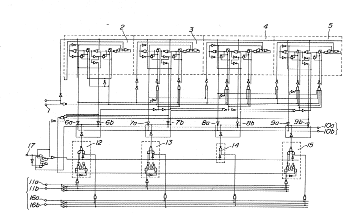
Fig. 1 shows a circuit arrangement which
characterizes the present invention. This
arrangement includes input terminals which are
arranged to receive clock pulses from a liquid
crystal type clock pulse generator tnot shown);
frequency dividers 2 - 5; gate circuits 6a, 6b, 7a,
7b, 8a, 8b and 9a, 9b; clock pulse output terminals
10a, 10b; gate control signal generator circuits 12 -
15; designated signal input terminals lla, llb, 16a
and 16b; and a discrimination signal input terminal
17 which is arranged to receive a signal from a
memory address decoder, all connected as shown.
With this arrangement the first frequency
divider 2 is arranged to perform a first division
(1/2) and divide the inpu-t pulses la shown in Fig.
2A, in a manner to produce a pulse train 2a such as
shown in Fig. 2B. The second pulse divider 3 is
arranged to perform a second division ~ and produce
a pulse train having a frequency 1/4 of the original
one. Viz., produce a signal 3a of the nature shown in
Fig. 2C.
The third and fourth frequency dividers
are arranged to perform subsequent frequency
divisions and produce signals 4a and Sa (see Figs.
2D, 2E) which respectively have frequencies which are
1/8 and 1/16 of the input signal la. As will be
' noted each of the clock pulses are arranged to be
formed with a 90 phase difference.
The outputs of the frequency dividers 2 -
5 are respectively supplied through the gate circuits
6a 9b to the clock signal output terminals 10a,
10b.
A two bit digital signal from the computer
control circuit i9 suQplie~ to the designated input
- .
.
,,
.
.
.
-- 5 --
terminals lla, llb. This signal functions to
selectively control the gate circui-ts 6a - 9b. Viz.,
when both of the signals appearing on the terminals
lla and llb, assume a low level "0" gate 6a, 6b is
5switched to assume an ON condition whereby the clock
pulses 2a which have been (1/2) divided appear on the
clock pulse output terminals 10a, 10b. When the
levels on the -terminals lla and llb assume low and
high levels ( 0, 1) respectively, ~ate circuit 7a, 7b
10is selectively conditioned to assume an ON state.
Under these conditions clock pulse train
3a is supplied to the clock pulse output terminals
10a, 10b.
In -the event that the signals appearing on
15terminals lla and llb assume levels 1 and 0, gate
circuit 8a, 8b is opened and the clock pulses 4a are
selectively appl~ied to terminals 10a, 10b. Finally,
if the signals appearing on the terminals lla, llb
both assume high levels (viz., 1, 1) then the last of
20the gate circuits is conditioned to open and apply
the (1/16) divided pulse train 4a to terminals 10a,
10b.
When a ~two bit signal from an external
memory is applied to the terminals 16a and 16b, a
~ 25similar control wherein the gate control circuits 12
`~ ~ to 15 selectively open the gates 6a - 9b is possible.
In the case that the ex-ternal memory is
selected and a discrimination signal is applied to
' terminal 17 therefrom, the gate control circuits 12
30to 15 are selectively conditionable to open the gate
circuits 6a to 9b.
When the above disclosed circuit
~; arrangement is put~into operation in a manner wherein
th0 high speed clock pulses 2a are changed to those
35shown in Fig. 2E (viz., 5a), low level signals are
applied to both the terminals lla and llb. This
~ . ,
.
~88~B
-- 6 --
induces gate control circuit 12 to apply a high level
signal (1) and condition gate 6a, 6b to assume an ON
state. Under these conditions high speed pulses are
applied to the output terminals 10a, 10b in the
manner illustrated in Fig. 2F and are supplied to the
CPU of the microprocessor.
In the event that the control circuit of
the microprocessor applies high level signals (1, 1)
to both of the terminals lla and llb, the gate
control circuit 15 is conditioned to apply a high
level signal to the gate 9a, 9b and thus open the
same. This results in the pulses appearing on the
clock pulse output terminals 10a, 10b to assume the
form shown in the latter half of Fig. 2F.
As both of these signals have been derived
from the same basic signal la when the change occurs,
as the trailing edges of the two signals are alinged
at the moment of switching, no shift in signal timing
can occur and disturb the operation of the
microprocessor.
In the case that the reverse change is
indu~ed and low speed clock pulses are changed to
; high speed ones, the le~els of the signals applied to
terminals lla and llb are switched from 1, 1 to 0, 0.
At this time the gate 9a, 9b is rendered
non-conductive while the gate 6a, 6b is op~ned. The
results o~ this is shown in Fig. 2G. As will noted as
the ~CPU is responsive to the clock ~pulses the above
mentioned switching will be timed in accordance with
; 30 the currently supplied pulse train and thus, in this
instance, will wait ~or a trailing edge of the low
speed pulses before inducing the signal:level change
which will induce the supply of~high speed pulses.
As before, as the trailing edges of pulses 2a and 5a
are inherently aligned, upon the change the phasing
~ ~ of the two signals are perfectly matched ensuring
::: :
.
,
-- 7 --
error free CPU opera-tion.
In the case that a low speed external
memory access cycle i.s to induced, a high level
signal is applied from a memory address decoder (not
shown) is applied -to -terminal 17. Prior to this time
the program being run in the CPU controlled in
accordance with the high speed pulses 2a. However,
upon the application of the high level signal to
terminal 17 gate circuit ~a, 6b is closed and gate
circuit 9a, 9b rendered conductive. Under these
circumstances the clock pulses supplied change in the
manner illustrated in Fig. 2H and low speed clock
pulses are then fed to the CPU.
The high level signal applied to terminal 17 is
maintained for 1 memory cycle and is then
automatically swi-tched to low level. This switching
of course permits the resumption of the supply of
high speed clock pulses to the CPU to permit
appropriate processing.
In accordance with the above disclosed
: arrangement,it is possible to selec-tively supply four
different clock pulses simply by changing a two bit
signal. Accordinyly, when the device is required to
be operated on a low voltage source such as torch
batteries or the like, it is possible to from the 2a
pulses to the 5a ones. It is also possible to switch
: to the low speed pulses in the event of a blackout
without adverse effect on the operation of the
processor. Fu~ther, the present invention permits
~: 30 low speed external memory access bus cycle control
: with the same simple hardware.: Moreover, in the
event that a system includes a high speed memory in
: addition the above méntioned low speed type, the
instant invention facilitates appropriate clock signal
control without the need of additional circuitry and
increases the system throughput.
-- 8
It will be understood that the present
invention is not limited to a the illustrated
arrangement and that various changes and
modifications can be made without departing from the
scope of the instant invention is which limited only
the appended claims.
:
I
.
;:: '
~ ~ '
.,
.: ~ ' - . '
.
.