Note: Descriptions are shown in the official language in which they were submitted.
12~33~3
METERING PULSE GENERATORS
BACKGROUND OF THE INVENTION
l. Field of the Inventlon
This invention relates to metering pulse
generators and more particularly to devices for
installation on gas or water meters or the like to develop
electrical pulses for transmission to a remote monitoring
location. Metering pulse generators of the invention
supply pulses of controlled amplitude and width, require a
very low torque input, have minimal standby power
requirements and a long operating life. The generators are
quite compact and readily installed, are comparatively
simple in construction and operation and are manufacturable
at low cost.
2. Backqround of the Prior Art
Devices have heretofore been provided for
developing pulses in response to rotation of dial arms of
gas water or other utility meters or the like. For
example, the Sears U.S. Patent No. 4j470,010 discloses an
apparatus in which a dial arm of a meter engages a shoe
which is affixed to one end of a shaft to rotate the shaft
38~
-- 2 --
against the action of a coiled spring wrapped around the
shaft. At its opposite end, the shaft has a striker arm
portion which is engageable with a bar of piezoelectric
material to generate an impulse. The impulse i5
transmitted through wires to remotely located circuitry.
Many other types of metering pulse generators have been
provided but the results obtained have been generally
unsatisfactory and the devices have been complex, expensive
and relatively large in size and not easily installed. A
particular problem relates to energy consumption,
particularly when the metering pulses are to be transmitted
by devices designed for battery operation. For example, in
devices designed to transmit metering data to a utility
control center through a telephone line, it is desirable to
use batterie~ to avoid the trou~le, expens~ and possible
hazards of obtaining power from an AC line. At the same
time, it is desirable to minimize the expense of sending
out service personnel to replace batteries and it is
therefore desirable to minimize energy consumption and
extend battery life as much as possible.
SUMMARY OF THE INVENTION
This invention was evolved with the general
object of providing metering pulse generators which have
minimal ener~y consumption and which impose minimal
~5 mechanical loads on meters on which they are installed,
while reliably generating metPring pulses for transmission
to a remote location. It is also an object of the
invention to provide metering pulse generators which have a
vary compact size and which are easily installed and which
are also economically manufacturable.
In accordance with this invention, a sensor is
engaged and deformed by a metering element to develop an
electrical signal, the sensor preferably comprising a
deforma~le spring member and a sensing device directly
..~ , :'
, '
3 --
secured thereto. Thus, an electrical signal is directly
generated in response to movement of the metering element
and a simplified and compact device is provided. In
preferred embodiments, the spring member is of resilient
sheet material which is bent through engagement by a
metering element and a strip o~ piezoelectric material is
secured to the spring member to generate electrical signals
in response to bending thereof.
Very important features relate to the provision
of an amplifier device in close proximity to the sensor and
arranged to respond to the electrical signal developed by
the sensor to transmit an output pulse signal to a remote
location. Prefarably, the amplifier device and associated
circuit components are mounted directly on the spring
member and the spring member is of insulating material and
functions as a printed circuit board for connections
between the sensor and amplifier device and circuit
components.
In accordance with another important feature, the
sensor is arranged to develop a single high amplitude pulse
signal of one polarity and the amplifier device is switched
from a non-conductive state to a conductive state in
response to each high amplitude pulse signal applied
~5 thereto. Thus, there is significant energy consumption
only during development of the pulse signal.
~ Specific features relate to the development of
the single high amplitude pulse signal in a manner such as
to insure accurate and reliable metering. In generators
constructed in accordance with the invention, a bending
movement of the spring member is gradually ef~ected a~Jay
from an initial rest condition and then the spring member
is released to effect a rapid return movement to the rest
condition. The high amplitude pulse is developed during
,
~8~
4 60332-1875
the rapid return movement. In particular, with the piezoelectric
sensing device, the charge of one polarit~ developed during the
movement away from the rest condition is allowed to gradually leak
away, and the high amplitude pulse is developed in response ~o a
charge of the opposite polarity which is developed during the
rapid return movement.
Oscillations o~ the member and the possibility of
resultant multiple pulse generations are avoided by damping and
absorbing the energy of the spring member as it is rapidly
returned to the initial rest position. Preferred methods include
the absorption of energy in air which is entrapped between the
spring member to be pressurized and displaced during the return
movement and the provision of a stop structure which is engaged by
the spring member to absorb energy and limit any substantlal
excursion beyond the initial rest condition.
In accordance with a broad aspect o~ the invention there
is provided a pulse signal generating device for responding to
movements of metering elements or the li~e and transmitting pulse
signals to a monitoring station, said device comprising: sensor
means positionable to be engaged and deformed by a metering
element and to develop an electrical signal during movement of the
metering element throuyh a certain portion of a path of movement
thereof, and an amplifier device having input electrode means
coupled to said-sensor means and output electrode means arranged
~or coupling through connecting uire means to the monitoring
station, said sensor =eans comprising a spring member of resilient
sheet material having a terminal end portion for qxtending into
,, :
.
~28~
4a 60332-1875
the path of movement of the me~ering element to effect a bending
movement in one direction away from an initial rest condition and
a return movement in the opposite direction back ko said initial
rest condition, and deformation sensing means for developing an
electrical signal in response to bending movements of said spring
member, said spring member being so arranged and positioned in
said path of movement of said metering element as to gradually
effect said bending movement in said one direction and to
relatively rapidly effect said return movement to said initial
rest condltion after said metering element reaches a certain
position, and dampiny and oscillation inhibiting means for
controlling ~he duration of said return movement to control the
duration of the generated pulse signal and for inhibiting
oscillatory movement of said spring member following movement of
said spring member back to said initial rest condition.
This invention contemplates other objects, ieatures and
advantages which will become more fully apparent from the
following detailed description taken in conjunction with the
accompanying drawings.
BRIEE DESCRIPTION OF THE D~AWINGS
FIGURE 1 is a front elevational view showing a metering
pulse generator of the invention mounted on the face of a gas
meter;
FIGURE 2 is an isometric exploded view, showing the
construction of components of the pulse generator of FIG. 1 and
the manner of assembly thereof;
~d`
.
.
33~3
5 --
FIGU~E 3 is a cross-sectional view on an enlarged
scale and with certain thicknesses exaggerated, showing the
construction of a piezoelectric film transducer and the
mounting thereof on a spring member o-f the generator;
FIGURE 4 is a circuit diagram, showing
connections of components of the generator; and
FIGURE 5 is a front elevational view showing a
modified metering pulse generator of the invention and
diagrammatically showing the mounting thereof on a water
meter, but with a cover of the generator removed to show
the internal construction.
DESCRIPTION OF PREFERRED EMBODIMENTS
Reference numeral 10 generally designates a pulse
generating device which is constructed in accordance with
the principles of this invention. As shown in Figure 1,
the device 10 may be mounted on the face ll of a gas meter
12 and is designed to produce a pulse in response to each
rotation of a dial pointer 13. The illustrated device 10
includes a member 14 of resilient sheet material which
extends from a housing 15 and which has a terminal end
portion 14a engageable by the end of the dial pointer. In
the arrangement as shown in Figure 1, the pointer 13
rotates in a counter-clockwise direction and it engages the
mem~er 14 to effect a gradual bending movement of the
member 14 away from an initial rest position. When the
pointer 13 reaches a certain angular position, the
resiliency of the member operates to effect a relatively
rapid return movement of the member to an initial rest
position as shown~
.
,
~2~
The device 10 generates an electrical pulse
signal in response to the rapid return movement of the
spring member and has output terminals for connection to a
connector 15 at one end of a cable 17, for transmission of
the signal to a remote location which may be several feet
away. By way of example, the device 10 may be used to
transmit metering pulses to an automatic meter reader or
"AMR" which is arranged to periodically transmit metering
data through a telephone line to a utility control center.
The AMR is preferabl~ battery operated and it is highly
desirable that current consumption be minimized. Accuracy,
reliability and a long operating life are also extremely
important.
The housing 15 comprises a bottom cover or base
18 and a top cover 19 both of which may be injection-molded
plastic parts. Mounting arrangements may vary in
accordance with the type and construction of the particular
meter on which the device is mounted. In the illustrated
construction, a screw 20 has a shank extending through a
~0 slot 21 in an integral tab portion 22 of the base 18. The
slot 21 is ~longated in a direction generally parallel to
the member 14 and permits accurate adjustment of the
positional relationship of the member 14 relative to the
path of movement of the end of the meter pointer 13.
The bottom cover or base 18 also includes an
integral tab 24 at one end which extends along the lower
side of the member 14 and toward the free terminal end
portion 14a thereof. The tab 24 operates as a damping .
means to control the duration of the return movement of the
member 14 and to inhibit oscillation thereof. During such
return movement, a cushion of air is developed between the
member 14 and the tab 24 and is pressurized and displaced
to absorb a portion of the energy stored during bending of
' '', ~ ' ' , .
, ~
8~
the member 14 after which the member 14 engages the tab 24
to mechanically absorb the remaining energy.
Important features of the invention relate to the
development of the electrical pulse signals in response to
return movement of the spring member. A deformation
sensing means is secured to the spring member 14,
preferably comprising a very thin and lightweight
piezoelectric transducer 26 which is adhesively secured to
the upper surface of the spring member 1~. An electronic
amplifying device is also provided which is preferably a
field-effect transistor 28 mounted on the spring member 14
in close proximity to the transducer 26 and connected
thereto through circuitry which is also mounted on the
spring member.
In the illustrated device 10, the spring member
supports a resistor 29 and a rectangular package 30 which
contains two resistors. A pair of pins 31 and 32 are
provided which form output terminals and which extend
upwardly through openings 33 and 34 in a wall portion 35 of
the top cover 19 and into the connector 16 of the cable 17.
The pins 31 and 32 are inserted in holes in the spring
member 14 and, when the device is assembled, lower ends of
the pins engage in underlying recesses in the base 18, for
mechanical support and rigidity. A further feature is that
the spring member 14 is of an electrically insulating
material and forms a printed circuit board with traces of
copper or the equivalent formed thereon to provide
connections between the transducer 26, transistor 28 and
resistor 29 and the resistors in package 30. Thus the
spring member 14 performs a number of important functions
and a very compact a~sembly is provided.
The top cover 19 includes an upper wall portion
36 which is overlies the transistor 2B, resistor 29 and
- , . .
.
.
, - ' ' ' ' ' ' . ' ' .
.
~X~3~
resistor package 30. Cover 19 may be secured to the base
through a connecting screw 37 extended through a central
hole 38 in the cover 19 and thence downwardly through a
hole in the member 14 and into a hole in the base 1~. The
cover 19 is also formed with a 510t 3g in one end wall 40
and a similar slot in the opposite end wall for embracing
the spring member 14, and with a pair of notches 41 and 42
in one side wall 43 and similar notches in an opposite side
wall for receiving tabs 45 and ~6 which project from one
side of the member 14 and similar tabs which project from
the opposite side of the member 1~. Thus the member 1~ is
securely held in position relative to the housing 15.
After assembly of the transducer 26, transistor
28, resistor components 29 and 30 and pins 31 and 32 on the
member 14, electrical connections are effected, preferably
by wave soldering. As shown, the base 1~ is formed with
recesses 18a and 18b for providing space to receive
terminals and portions of the components which project from
the underside of the member 14.
Figure 3 is a cross-sectional view with
certain thicknesses exaggerated to show how the transducer
26 is constructed and assembled on the member 14. The
transducer 26 is in the form of a thin film of a
piezoelectrically active material and electrodes secured
~S thereto. By way o example it may preferably comprise a
polyvinylidene fluoride film 48 which is approximately
0.200 inches wide by 0.750 inches long and 28 microns thic~
and which has electrodes 49 and 50 silk-screened onto its
opposite faces. An adhesive 51 is provided between the
lower electrode 49 and the upper face of the member 14 to
secure the transducer 26 to the member 14. The adhesive 51
is a conductive adhesive to also function to provide an
electrical connection between the electrode 49 on the lower
face of tha film 48 and a copper trace 52 on the upper face
3~
_ 9 _
of the member. A connection 53 is similarly provided
between the upper electrode 50 and a copper trace 54 on the
member 14 which is electrically separate from the trace 52.
Figure 4 is a circuit diagram. As shown, the
transistor 26 is an N channel enhancement mode, metal oxide
field effect transistor or "MOSFET". It has a drain
electrode 55 connected to the pin 32 and to one terminal of
the resistor 29 and a source electrode 56 connected to the
pin 31, to the other terminal of resistor 29 and also to
the transducer electrode 49 through the trace 52. A gate
electrode 57 is connected to a terminal of one resistor 58
of the package 30, the other terminal of the resistor 58
being connected to the transducer electrode 50 through the
trace 54. A second resistor 60 of the pac~age 30 is
connected between traces 52 and 54, in parallel relation to
the transducer 26.
In operation, the film 48 develops a charge
between its opposite faces when deformed during bending of
the member 14. The film 48 is compressed during bending of
the member 1~ away from its rest position, developing a
charge having a polarity such that the voltage of the
electrode 50 is negative relative to the electrode 49. The
polarity of the charge so developed during bending is
opposite that required to cause conduction of the
~5 transistor 28. Such bending takes place relatively slowly
and the charge gradually bleeds off through the resistor
60.l When the spring member is released to move relatively
rapidly back to its initial rest position, the charge is
changed in the opposite directioh and a voltage is
developed at the electrode 50 which is of positive polarity
and which is such as to cause conduction of the transistor
28 for a certain time interval, dependent upon the amount
of deflection and the values and characteristics of the
components. When the voltage at the gate electrode 57 is
,~ ,
, . ;~ ' ' .
' :
.. ~
~2~
-- 10 --
sufficient to initiate conduction of ~he transistor 28, the
effective resistance between the gate and source electrodes
57 and 56 is relatively low as compared to the resistances
of the resistors 58 and 60. Consequently, the electrical
values which affect the conduction time are the values of
the resistors 58 and 60, the capa~itance of the transducer
26 and the voltaqe generated by the film during deflection,
the capacitance of transducer 26 and the generated voltage
being a function of the thickness and ef~ective area of the
film 48, its composition and the deflection thereof.
By way of illustrative example, and not by way of
limitation, the types and values of the components may be
as follows:
Reference number TYpe or value
:15 28 Silconix VN2222L
29 249,000 ohms
58 10 megohms
22 megohms
The film 48 of the transducer may be a
~a polyvinylidene fluoride film marketed by Pennwalt
Corporation under the trade ~ "KYNAR", approximately
0.200 inches wide, 0.750 inches long and 28 microns in
thickness. The spring member 14 may be a multilayer
epoxy/glass fabric laminate of a type used in conven~ional
cirduit boards, approximately 1.5 inches long, 0.200 inches
wide and 0.020 inches thick, with copper surface paths on
both surfaces and with holes for insertion of the terminals
or leads of the transistor and resistor components. After
wave soldering of the leads, a conformal coating is applied
to protect the assembly from the environment.
.
, ~ , ' , ' . :
..
12~
Only a very small force is required to obtain the
required deflection of the spring member 14 ~ut the desired
electrical pulse signals are generated with a high degree
of reliability. The duration of conduction of the
transistor 26 may range from 2 to 20 milliseconds depending
upon the deflection of member 14. The resis~ance between
the pins 31 and 32 may be on the order of 7.5 ohms during
conduction of the ~ransistor 28 and is substantially the
same as that of the resistor 29, i.e. 249,000 ohms, during
non-conduction of the transistor 28.
With the aforementioned mechanical damping and
electrical characteristics, clean and uncluttered
electrical pulse signals can be transmitted through
substantial distances to a monitoring station and a very
reliable and trouble-free metering operation is obtained.
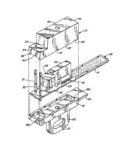
Figure 5 is a view illustrating portions of a
modified device 62, shown with a cover thereof removed and
shown in relation to a rotating meter element 63. Element
63 may be an element of a water meter, for example, to be
rotated in proportion to the volume of water flowing
through a metering mechanism. As shown, it has 10
arcuately spaced cam fingers 64 on its periphery which are
engageable with a terminal end portion 65 of a spring
member 66 of the device 62.
~5 Spring member 66 of device 62 is like the member
14 df the device 10 and has transducer and circuit
components mounted thereon in the same way, including a
piezoelectric film transducer 68 like transducer 26, a
field-effect transistor 69 like transistor 28, a pair of
resistors in a package 70, corresponding to resistors 58
and 60 in package 30, and an additional resistor which is
not seen in Figure but which is like resistor ~9 and
behind the package 70. A pair of pins which are like pins
, ~
- 12 -
31 and 32 are secured to member 66 adjacent one end thereof
to form output terminals, as indicated by reference numeral
71.
A housing 72 is provided which is ~ormed with
slots 72a and 72k for receiving screws to mount the device
on the face o~ a meter. The housing 72 is formed to
provide a slot for receiving and supporting the member 66
in a slightly bowed configuration when in an initial rest
condition thereof, the member 66 being engaged by a
shoulder 73 and two ribs 74 and 75 which extend
transversely relative to the member 6~ at longitudinally
spacad positions. The shoulder 73 engages the underside of
the end portion o~` the member 66 adjacent the pins 71. The
rib 74 engages a portion of the spring member 66 which is
spaced from the terminal end portion 65 thereof engaged by
the cam fingers 64. The rib 75 engages the upper side of
the member 66 at a position which is intermediate the
shoulder 73 and the rib 74, in the longitudinal direction,
and is located below a plane through the shoulder 73 and
~O the rib 74, thereby holding the member 66 in a bowed
condition.
When the meter element 63 is rotated, each of the
cam fingers 64 engages the terminal end portion of the
spring member 66 to move the spring member 66 upwardly away
~5 from the rib 74, a fulcrum point being provided by the rib
75. When each cam finger 64 reaches a certain position,
the'member 66 is released to move rapidly back toward the
initial rest position as illustrated, and a high amplitude
pulse is generated by the transducer 68 o a polarity such
as to cause conduction of the transistor 69. When the
spring member 66 reaches the initial rest position, it
engages the rib 74 which absorbs energy and limits any
substantial sxcursion beyond the rest condition. The
arrangement prevents any deformation of the transducer 68
, .. , ~ .
:.: - . , .
,
, ' ~ ,
, ' , '
1;~8~B~
- 13 -
which might produce a pulse of an amplitude and polarity
such as to cause development of a secon~ pulse. The result
is that a single and very clean high amplitude pulse is
generated in response to movement of each cam finger into
engagement with the member 66.
It will be understood that modifications and
variations may be effected without departing from the
spirit and scope of the novel concepts of this invention.
.
;- ,
;,
: ,