Note: Descriptions are shown in the official language in which they were submitted.
;o~
The invention relates to optical logic devices
and assemblies for carrying out a logic function on an
incident optical signal.
Optical logic i5 most often proposed u~ing
active optical components such as bistable devices using
laser diode6 and photodiodes, laser amplifiers operating
with feedback to achieve bistability, ~elf electro-optic
effect devices (SEED), holograms and liquid crystal light
valves. Some optical logic devices have included
wavegides which have a non-linear refractive index so that
an incoming light signal switches between output paths in
accordance with the intensity of the signal.
The main problems with these devices are their
complexity and in some cases the need for feedback. Also,
it is not easy to monitor the optical signals.
In accordance with the present invention, an
optlcal logic device comprises an optical logic device
comprises: a source of substantially constant optical
power, optical signal output means to which the optical
power is fed, the optical signal output means having at
least one output port and being responsive to electrical
control signals selectlvely to génerate optical signals on
its at least one output port, optical signal input means
to which an incoming optical signal is fed, and detection
means for detecting an optical signal fed to the optical
signal input means and for generating a corresponding
electrical control signal limited in magnitude to a
,predetermined maximum value by a buffer limiting device
and coupled to control the optical signal output means so
ithat the optical condition of the output port 1~ changed
in the opposite sense to the incoming optical signal.
According to a ~urther aspect of the invention
in an optical signal inverter having an optical-
electrical-opticai lnterface wherein an optical output
signal i~ switched under control of an electrical control
signal generated by detection of an incoming optical
8 i gnal, the improvement comprises: electrical signal
buffering means for limiting the magnitude of the
electrical control signal to no more than a predetermined
maximum value which is below the value otherwise produced
by incoming optical signal(s) in excess of a predetermined
optical intensity.
This logic device i5 based on the principle of
providing an electronic interface between the incoming
optical signals and the outgoing optical signals. This
means that no optical feedback i5 required and enables
very fast component parts to be used. Potentially, very
high speed~ may be obtained, po~sibly of the order o a
few tens of pico seconds. The power consumption o~ the
device may be only a few tens of mW at several GBit/s
operating speeds. This should be compared with co~nercial
~CL which has typical power disslpation per gate of about
50mW but at only a few hundred MBits/s.
A fur~her advantage of the invention i8 that the
optical power generation i~ xemote ~rom the other
components of the device and thus the to~al dissipation
is simply that of the detection means since in practice
the dissipation of the optical signal output means will
be negligible. Also, the operation of the device is not
dependant upon the optical source wavelength to any
marked degree. Elowever, it is preferable if the source
generates an incohexent optical beam so that destructive
interference does not occur at the optical signal output
means.
The logical value of the input optical signal and
the output optical signal will be determined by external
factors. In the simplest case, the presence of an
optical signal may represent one logical condition wh~le
the absence of an opt~cal siqnal may represent the
complementary logical condition. Alternatively, a
non-zero threshold may be set so that optical signals
having an intensity greater thaTI the threshold will
represent one logical con~ition while optical signals
having an intensity equal ~o or less than the threshold
will represent the complementary condition. Furthermore,
different definitions can be used for the input signals
and the output signals.
Monitoring of the high speed optical signals may be
achieved by fabricating low coupling ratio directional
couplers in the optical paths where required. Such
monitoring will not substantially compromise the logic
2~
circuit performance in contrast to what may occur wi~h
electronic logic at very high speed,
Preferably, the optical signal output means ha~ two
output ports, the optical conditions of the output p~rts
5 ~eing changed in opposite sen~es ~n response to the same
electrical control signals.
This is particularly advantageous since the device
will then produce logically complemen~ary outputs
automatically.
Preferably~, the optical signa1 output means
comprises a wavequide ~witch.
The detection means may comprise a photodetector
which is convenien~ly electrically connected to a buffer
limiting device~ The advantage o~ providing a buffer
limiting device w'ill be explained in more detail below.
The invèntion in its simplest form defined above
comprises an optical inverter. Any logic function can be
obtained by using a combination of inversion and
combinillg functions and in one particularly convenient
arrangement, the device further comprises optical signal
coupling means for coupllng two input optical signals and
for feedin~ the ~esultant coupled signal to the optical
signal input means. This arrangement allows OR and NOR
functions to be obtainea. In this case, it 1~
advan~a~eous to provide a buffer llmiting device since
when the input optical siynals both have a significant
power value this could result in the detection means
generating an undesira~ly high electrical control signal.
The buffer limiting device prevents this from happening.
The bas~c building block of the inven-tion can be
used in a variety of ways to form more complex loqic
assem~lie~. In one example of such a lo~ic assembly a
conunoll 60urce of substantially constant optlcal power is
provided, This is a partisularly advantageous feature
8~
which enables long signal delays to be avoided and
simplifie6 the overall construction of the assen~ly.
In this specification the term optical is intended
to refer to that part of the electro-magnetic spectrum
which is generally known as the visible region together
with those parts of the infra-red and ultra-violet
regions at each of the visible region which are capable
of being transmitted by dielectric optical waveguides
such as optical fibre~.
The main advantages of the invention may be
summarised as follows:-
i there i~ no optical feedback for the basic gate
functions .
ii it does not rely on bistability of optical
device6
iii more complex logic functions are configurable
rom the basic gate using simple fibre or waveguide
interconnections.
iv it is conceivable tllat tlle optical logic block
could be monolithically integrated.
In order that the invention may be better
understood, two examples of loglc devices and an assembly
including the devices accordingto the islvention will now
be described with reference to the accompanying drawings,
25j in which:-
Figure 1 is a schematic, perspective view of anoptical inverterS
Figure 2 illustrates an optical OR/NOR gate; and,
Fiqure 3 illustrates a logic assembly providing
30 OR,NOR, ~ND and NAND functions.
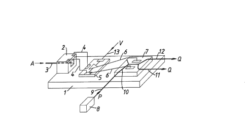
The optical inverter shown in Figure 1 comprises a
~ase 1 on which is mounted a photodetector 2. An optical
fibre or planar wavequide 3 carries an input optical
signal "A" which is applied to the photodetector 2. The
photodetector 2 i~ connected via electrical wires 4 with
a current to voltage buffer clrcuit 5 which is
conveniently provided with a voltage limiting capability.
The voltage buf~er circuit 5 is connected via
electrical wires Ç to an optical waveguide switch 7 of
conventional ~orm. A la~er assembly 8 generates an
incoherer~t ~eam of optical radiation which i5 fed along
an optical waveguide such as an op~ical f~bre 9 to one
input port 10 of the wavegu~de sw~tch 7. The switch 7
has two output ports 11, 12 to which optical power
received on the input port 10 i5 selectively coupled
depending upon the potential di~ference on the wires 6.
' Electrical dc power is applied to the voltage buffer
- circuit 5 via a voltage input 13.
The optical signals output fxom the ports 11, lZ are
arranged to have logical conditions which are
re~pectively complemental and the same as the logical
condition of the input optical slgnal ~A". It is ~he
optical signal output from the port 11 which is the more
important since this iB the inverse or logical complement
20 O~ the input signal.
The transfer function and propagation delay of the
inverter shown in Fiyure 1 are dependant upon the logic
levels required. The power P from the laser assembly 8
is required to be as high as possible to minimise the
buf~er circuit 5 complexity ~o that the propagation
delay, .a critical parameter in lo~ic de~ign, is
minimised.
If the switching voltage for the waveguide ~witch is
V~, the photodetector responsivi~y is X and the buffer
transresistance is T~ then the opt~ca~ logic power level
Pl i~ given by.,
V W
P - g
--
XT
If Vs ~ 5. X - lA/W and T = 50n
then Pl 3 l00mW
T~1is rather high level of optical power may be
recluced if a hlgher buffer transresistance is prov~ded.
For instance for a transresistance of 50011 the optical
power level reduces to l0mW. The u~e of a detector with
scme internal gain, such as a photoconductor or avalanche
p}1otodiode, may allow reduction o~ the required optical
power or transresi~tance.
The progagation delay is the addition of the delay
through the fibre or planar waveyuide inputs and outputs
and the delay in the photodetector, buffer and switch.
To minimise this delay an optimisation i~ required to set
values for the optical power level and transresistance.
The optical power (cw) could be generated in a high power
cw laser or other light source and distributed to the
inverters using fibres and/or planar waveguides.
A logic device ba~ed on the device shown in ~igure l
i8 illustrated in Figure 2. The inverter o~ Figure l is
indica-ted at 14 and it will be seen that the optical
fibre 3 is coupled with an optical coupler 15 having two
inputs connected to optical fibres 16, 17 respectively.
The assembly shown in Figure 2 operates on the two
incoming optical signals "A" and "B1' so that the optical
~ignal output from the port ll represents A OR B. The
output from th~ port l~ represents A NOR B.
It should be understood that in a simple case one
logical condition will be repxesented by the absence of
an optical signal while the other logical condition is
represented by the presence of an optical signal.
The truth table for the assembly ~hown in Figure 2
i~ given below.
3~
~28~
TABLE
A B C
O O O
0
0
A logic assembly i~ illustrated in ~igure 3. This
assembly comprises four optical lnverters similar to that
shown in Figure 1 labelled 18-~1. The optical inverters
18, 19 receive input optical ~ignals ~ and generate
corresponding logically complemental output siqnals A, A;
and B, B respectively. The A and B output signals are
fed to an optical coupler 22 connected to th~ input port
of the optical inverter 20. ~he outputs ~ and B are fed
to an optical coupler 23 connected to an input port ~f
the optical inverter 21. The optical inverters 20, -~1
have a total of four output ports whose logica~
conditions represent A OR B, A NOR B, A NAND B, and A AND
~ respectively.
In a modification ~not s}lown) the 6ignals A, B could
be split prior to reaching the invertors 18, 19 and be
~ed additionally directly to the coupler 22.
The optical inverter forming the basic building
block of the in~ention is simple and it m~y be possible
to fabricate arrays of the {nverter~ which could be "hard
ibred" ~or specific functions. Thi~ leads to the
pos~ibility that an assembly ~uch as that shown in Figure
3 could be reprodu~ed as a monolithic array allowing a
range of MSI or LSI functions to be achieved.