Language selection

Search

Patent 1289207 Summary

Third-party information liability

Some of the information on this Web page has been provided by external sources. The Government of Canada is not responsible for the accuracy, reliability or currency of the information supplied by external sources. Users wishing to rely upon this information should consult directly with the source of the information. Content provided by external sources is not subject to official languages, privacy and accessibility requirements.

Claims and Abstract availability

Any discrepancies in the text and image of the Claims and Abstract are due to differing posting times. Text of the Claims and Abstract are posted:

  • At the time the application is open to public inspection;
  • At the time of issue of the patent (grant).
(12) Patent: (11) CA 1289207
(21) Application Number: 565828
(54) English Title: MICROWAVE ABSORBER ATTENUATOR FOR LINEAR SSPA POWER CONTROL
(54) French Title: ABSORBEUR DE MICRO-ONDES SERVANT A LINEARISER LA REPONSE FREQUENTIELLE D'UN AMPLIFICATEUR DE PUISSANCE A SEMICONDUCTEUR
Status: Deemed expired
Bibliographic Data
(52) Canadian Patent Classification (CPC):
  • 333/86
(51) International Patent Classification (IPC):
  • H01P 1/22 (2006.01)
  • H03F 1/32 (2006.01)
  • H03F 3/21 (2006.01)
  • H03F 3/60 (2006.01)
  • H03G 3/20 (2006.01)
  • H03G 11/04 (2006.01)
(72) Inventors :
  • MCGANN, WILLIAM E. (United States of America)
  • TODD, JOHN R. (United States of America)
(73) Owners :
  • AMERICAN TELEPHONE AND TELEGRAPH COMPANY (United States of America)
(71) Applicants :
  • MCGANN, WILLIAM E. (United States of America)
  • TODD, JOHN R. (United States of America)
(74) Agent: KIRBY EADES GALE BAKER
(74) Associate agent:
(45) Issued: 1991-09-17
(22) Filed Date: 1988-05-03
Availability of licence: N/A
(25) Language of filing: English

Patent Cooperation Treaty (PCT): No

(30) Application Priority Data:
Application No. Country/Territory Date
045,414 United States of America 1987-05-04

Abstracts

English Abstract


ABSTRACT OF THE DISCLOSURE
The nonlinearity of the frequency response of a solid
state power amplifier (SSPA) is obviated by effectively
operating the SSPA at the ldB compression point, where the
nonlinearity does not exist, and controllably reducing,
downstream of the SSPA, the power output produced by the SSPA
to the level required by the link. In particular, the output
is reduced by controllably inserting a relatively thin tapered
blade of ferrite material into a waveguide coupling section
downstream of the SSPA. Preferably the ferrite material is
comprised of a robust carbonyl steel of sufficient thickness
to withstand the heat induced in the course of its absorbing
microwave energy at the SSPA output, while being of a narrow
or thin configuration and oriented for insertion into the
absorbing section of waveguide so as to not effectively alter
the characteristics of the signal profile of the
electromagnetic wave.


Claims

Note: Claims are shown in the official language in which they were submitted.


The embodiments of the invention in which an exclusive
property or privilege is claimed are defined as follows:

1. For use with a signal amplification network through
which input signals to be transmitted over a communication
link are coupled, said network including a signal
amplification device the frequency response of which has a
first characteristic for a first output level of said device
and a second characteristic for a second output level of said
device, a method of operating said network such that signals
coupled therefrom effectively correspond to the second output
level of said device but the frequency response of which has
said first characteristic comprising the steps of:
(a) operating said signal amplification device such that
the signal output level thereof corresponds to said first
output level at which the frequency response thereof has said
first characteristic; and
(b) adjusting the level of the signal output produced by
said signal amplification device to said second output level.
2. A method according to claim 1, wherein step (b)
comprises adjusting the level of the signal output produced by
said signal amplification device in accordance with a
variation in one or more a prescribed operational
characteristics of said communication link.
3. A method according to claim 1, wherein said first
frequency response characteristic corresponds to a
substantially flat power output over the frequency range of

- 12 -


operation of said device and said second frequency response
characteristic corresponds to a nonlinear power output over
the frequency range of operation of said device.
4. A method according to claim 3, wherein said step (b)
comprises absorbing a controlled amount of the signal energy
produced at the output of said device so as to reduce the
level of the signal output from first level to said second
level.
5. A method according to claim 4, wherein said device
comprises a solid state power amplifier and step (a) comprises
operating said solid state power amplifier at a gain whereat
the frequency response characteristic of said amplifier is
substantially flat.
6. A method according to claim 5, wherein step (b)
comprises coupling the output of said solid state power
amplifier through a section of waveguide downstream thereof,
and controllably inserting a microwave absorber into said
section of waveguide so as to reduce the signal level to a
level less than said first level.
7. A method according to claim 6, wherein said
microwave absorber comprises a body of material having tapered
leading and trailing surfaces extending in the direction of
transmission of microwave signals through said section of
waveguide.
8. A method according to claim 7, wherein said tapered


- 13 -


surfaces taper to leading and trailing edges of said absorber
such that microwave signals travelling through said section of
waveguide gradually encounter the bulk of the material of said
absorber.
9. A method according to claim 8, wherein said absorber
is controllably inserted into a slot in said section of
waveguide whereat the magnitude of the electric field vector
is at a maximum.
10. A method according to claim 1, further including the
steps of
(c) storing information representative of the variation
in the manner in which said signal amplification network
couples signals therethrough over a range of variation of at
least one prescribed operating parameter; and
(d) modifying input signals coupled to said signal
amplification device in accordance with information stored in
step (c).
11. A method according to claim 10, wherein the
information stored in step (c) is representative of the
variation in gain of said signal amplification network for
variations in ambient temperature thereof, and step (d)
comprises controllably adjusting said input signals as a
complementary function of said variation of gain with
temperature.
12. A method according to claim 11, further including


- 14 -


the steps of
(e) modifying input signals coupled to said signal
amplification device in accordance with a prescribed
transmission characteristic of said communication link.
13. A method according to claim 12, wherein said
prescribed transmission characteristic of said communication
link corresponds to attenuation of signals thereover during
the transmission signals over said link.
14. A method according to claim 13, wherein step (e)
includes monitoring a signal representative of the carrier
level of signals received downlink of said network which will
compensate for fades in the uplink by increasing the uphigh
powers proportion to the detected downhigh fades.
15. An electromagnetic wave absorber comprising a body
of electromagnetic energy absorbent material having a central
body section opposite surfaces of which are substantially
parallel to one another and a pair of tapered body sections
extending from said central body section.
16. An electromagnetic wave absorber according to
claim 15, wherein each of said tapered body sections has a
pair of surfaces respectively tapered from the parallel
opposite surfaces of said central body section to an edge
portion thereof.
17. An electromagnetic wave absorber according to
claim 16, wherein the entirety of said control body section

- 15 -


and said tapered body sections are made of a ferrite-based
electromagnetic energy absorbent material.
18. An electromagnetic wave absorber according to
claim 15, further comprising a section of waveguide having an
aperture in a wall portion thereof and means for controllably
inserting said body of electromagnetic energy absorbent
material through said aperture into the cavity of said section
of waveguide.
19. An electromagnetic wave absorber according to
claim 18, wherein said body is arranged to be inserted into
the cavity of said section of waveguide such that said tapered
body sections extend in the longitudinal direction of said
section of waveguide.
20. An electromagnetic wave absorber according to
claim 16, wherein each of the tapered surfaces of each of said
tapered body sections has an effectively exponential varying
slope between a parallel opposite surface and an edge portion.
21. For use with a signal amplification network through
which input signals to be transmitted over a communication
link are coupled, said network including a signal
amplification device the frequency response of which has a
first characteristic for a first output level of said device
and a second characteristic for a second output level of said
device, an arrangement for operating said network such that
signals coupled therefrom effectively correspond to the second


- 16 -


output level of said device but the frequency response of
which has said first characteristic comprising:
first means for operating said signal amplification
device such that the signal output level thereof corresponds
to said first output level at which the frequency response
thereof has said first characteristic; and
second means, coupled to the output of said signal
amplification device, for adjusting the level of the signal
output produced by said signal amplification device to said
second output level.
22. An arrangement according to claim 21, wherein said
second means comprises means for adjusting the level of the
signal output produced by said signal amplification device in
accordance with a variation in a prescribed operational
characteristic of said communication link.
23. An arrangement according to claim 21, wherein said
first frequency response characteristic corresponds to a
substantially flat power output over the frequency range of
operation of said device and said second frequency response
characteristic corresponds to a nonlinear power output over
the frequency range of operation of said device.
24. An arrangement according to claim 23, wherein said
second means comprises means for absorbing a controlled amount
of the signal energy produced at the output of said device so
as to reduce the level of the signal output from first level


- 17 -


to said second level.
25. An arrangement according to claim 23, wherein said
device comprises a solid state power amplifier and said first
means comprises means for operating said solid state power
amplifier at a gain whereat the frequency response
characteristic of said amplifier is substantially flat.
26. An arrangement according to claim 25, wherein second
means comprises a section of waveguide coupled the output of
said solid state power amplifier, and means controllably
inserting a microwave absorber into said section of waveguide
so as to reduce the signal level to a level less than the gain
level whereat the frequency response characteristics of said
amplifier is substantially flat.
27. An arrangement according to claim 26, wherein said
microwave absorber comprises a body of material having tapered
leading and trailing surfaces extending in the direction of
transmission of microwave signals through said section of
waveguide.
28. An arrangement according to claim 27, wherein said
tapered surfaces taper to leading and trailing edges of said
absorber such that microwave signals travelling through said
section of waveguide gradually encounter the bulk of the
material of said absorber.
29. An arrangement according to claim 28, wherein said
second means includes means for inserting said absorber into a

- 18 -


slot in said section of waveguide whereat the magnitude of the
electric field vector is at a maximum.
30. An arrangement according to claim 21, further
including
third means for storing information representative of the
variation in the manner in which said signal amplification
network couples signals therethrough over a range of variation
of at least one prescribed operating parameter; and
fourth means for modifying input signals coupled to said
signal amplification device in accordance with information
stored by said third means.
31. An arrangement according to claim 30, wherein the
information stored by said third means is representative of
the variation in gain of said signal amplification network for
variations in ambient temperature thereof, and said fourth
means comprises means for controllably adjusting said input
signals as a complementary function of said variation of gain
with temperature.
32. An arrangement according to claim 31, further
including
fifth means for modifying input signals coupled to said
signal amplification device in accordance with a prescribed
transmission characteristic of said communication link.
33. An arrangement according to claim 32, wherein said
prescribed transmission characteristic of said communication


- 19 -


link corresponds to attenuation of signals thereover during
the transmission signals over said link.
34. An arrangement according to claim 33, wherein said
fifth means includes means for monitoring a signal
representative of the carrier level of signals received
downlink of said network.
35. An electromagnetic wave attenuation control device
for use in a communication link, said device comprising:
(a) a section of waveguide;
(b) an electromagnetic wave absorber comprising a body
of electromagnetic energy absorbent material extending into
said waveguide;
(c) means for supporting said body within said waveguide
at a location corresponding to an energy absorbent condition,
including means for adjusting the location of said body within
said waveguide; and
(d) means for controlling said adjustment means in
response to one or more prescribed operational characteristics
of the communication link.
36. The device set forth in claim 35, wherein said
control means is responsive to changes in the uplink power
requirements in the satellite communications link.
37. The device set forth in claim 35, wherein said
control means is responsive to changes in the power level of
the electromagnetic radiation transmitted by said waveguide.


- 20 -


38. The device set forth in claim 35, wherein said
control means is responsive to changes in the power level of
the electromagnetic energy being transmitted by said waveguide
and to changes in uplink power requirements in the satellite
communications link.

- 21 -

Description

Note: Descriptions are shown in the official language in which they were submitted.


~ 2~


FIELD OF THE INVENTION
_
The present invention relates in general to satellite
communication systems, and is particularly directed to a
scheme for controlling the output power of a microwave solid
state power amplifier through the use of ferrite absorber
element, the insertion of which into a section of output
waveguide is adjustable.

BACXGROUND OF THE INVENTION
. . _
Because of its low cost and compact size, the solid state
(GaAsJ power amplifier ~SSP~3 is a commonly employed component
of the uplink transmitter of a VSAT (very small aperture
terminal) Ku band earth station. The (gain) transfer (power
output vs. power input) characteristic of a typical SSPA has a
positive sloped linear region which gradually decreases over a
knee portion to a slightly negative-sloped saturation region.
When driven at the l.OdB gain compression point, namely at
that point on the knee of the transfer characteristic which is
ldB below an extension of its linear, positive slope region,
th;e frequency response of the SSPA has a substantially smooth
profile over its intended operational range.
For currently available SSPAs the output power at the lds
gain compression point is on the order of two watts, which may
be considerably greater than the power required by the
link (e.g. one watt~. Consequently, it is necessary to reduce
the output power transmitted by the uplink terminal. Ideally,

I

)7


this power reduction would be accomplished by simply reducing
the input power to the SSPA, as its output linearly tracks its
input over the linear portion of its transfer characteristic
below the ldB compression point. Unfortunately, the frequency
response of the SSPh does not follow suit. Instead, thé
frequency response drastically departs from the smooth flat
profile at ldB compression and ripples significantly across
the transmit passband.
In the prior art there is described a signal processing
scheme for compensating for this nonlinear frequency response
and additional performance variables (e.g. gain vs.
temperature) which essentially comprises a preemphasis
mechanism inserted upstream of the SSPA. Now, while the
nonlinearity compensation scheme described in the prior art is
certainly a useful technique for solving the nonlinearity
problem, it would be preferred, if possible, to operate the
SSPA in such a manner to avoid the problem altogether.
SUMMARY OF THE INVENTION
Pursuant to the present invention, the objective
discussed above is achieved by effectively operating the SSPA

07

the ldB compression point, where the passband ripple doDs
not exist, and controllably reducing, downstream of the SSPA,
the power output produced by the SSPA to the level required b~
the link. In particular, the present invention is directed to
a mechanism for controllably inserting a relatively thin
tapered blade of ferrite material into a waveguide coupling
section downstream of the SSPA. Preferably the ferrite
material is comprised of epoxy-bonded carbonyl steel particles
of sufficient thickness to withstand the heat induced in the
course of its absorbing microwave energy at the SSPA output,
while being of a narrow or thin configuration and oriented for
insertion into the absorbing section of waveguide so as to not
effectively alter the characteristics of the signal profile of
the electromagnetic wave.
In accordance with one aspect of the invention there is
provided for use with a signal amplification network through
which input signals to be transmitted over a communication
link are coupled, said network including a signal
amplification device the frequency response of which has a
first characteristic for a first output level of said device
and a second characteristic for a second output level of said
device, a method of operating said network such that signals
coupled therefrom effectively correspond to the second output
level of said device but the frequency response of which has
said first characteristic comprising the steps of: (a~
operating said signal amplification device such that the
signal output level thereof corresponds to said first output
level at which the frequency response thereof has said first


07

aracteristic; and (b) adjusting the level of the signal
output produced by said signal amplification device to said
second output level.
In accordance with another aspect of the invention there
is provided an electromagnetic wave absorber comprising a body
of electromagnetic energy absorbent material having a central
body section opposite surfaces of which are substantially
parallel to one another and a pair of tapered body sections
extending from said central body section.
BRIEF DESCRIPTI~N OF THE DRAWINGS
Figure l is a diagrammatic illustration of a VSAT power
amplifier section incorporating a waveguide attenuator in
- accordance with the present invention;
Figures 2 and 3 are respective sectional side and end
views of the attenuator waveguide section 14 shown in Figure 1
depicting the manner in which the attenuator element-is
inserted into the waveguide section; and
Figure 4 is a cross-sectional view of the attenuator
element 33 employed in the attenuator waveguide section shown
in Figures 2 and 3.


.


DETAILED DESCRIPTION
.
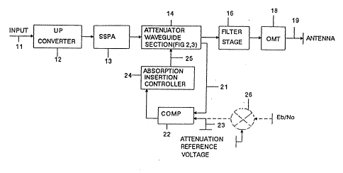
~ eferring now to Figure 1, there is illustrated a
schematic ~loc~ diagram of a power control section containing
a solid-state power amplifier and attenuator waveguide section
incorporated in the up-converter circuitry between the IF
input and ~F output of a VSAT earth station.
More specifically, an input signal (e.g. an intermediate
frequency signal having a frequency of 190MHz) is coupled to

an up-converter 12 of the earth station transmitter. The
10 output of up-converter 12 has a frequency corresponding to the
transmission frequency of the earth terminal, as beamed from
the earth terminal antenna to the satellite. For purposes of
the present description, it will be assumed that this output
frequency lies in a Ru band range of 14.0-14.5GHz. The
up-converter 12 is coupled to a solid state power amplifier
(SSPA) 13, the output of which is coupled to an attenuator
waveguide section 14, the details of which will be described
below in conjunction with the description of Figures 2 and ~.

Attenuator waveguide section 14 serves to controllably
attenuate the output of SSPA 13 to the level required by the
satéllite link. As mentioned briefly above, SSPA 13 is
operated at its ldB gain compression point so that its
frequency response is substantially flat over the range of
frequencies of interest (e.g. 14.0-]4.5GHz).
~5 The output of waveguide section 14 is coupled through a


-- 4

~8~


waveguide filter stage 16 to an orthomode transducer 1~.
Waveguide filter stage 16 is comprised of a pair of cascaded
filters, specifically a harmonic output rejection filter for
SSPA 13 and a receive band noise power rejection filter. The
output of orthomode transducer 18 is coupled over link 19 to
an antenna feedhorn (not shownl.
As mentioned above, the behavioral characteristics of a
typical SSPA 13 are such that its gain varies considerably
with a change in frequency when operated below its ldB gain
compression poin~. Pursuant to the present invention, SSPA 13
is operated at its ldB gain compression point so that its
output characteristic is substantially flat over the frequency
range of interest. For present day VSAT stations, operating
in the Ku b~nd, the output power of the terminal may be on the
order of several watts or less. (Typically, for a
commercially available gallium arsenide SSPA,-its ldB gain
compression point produces an output on the order of two
watts.) The power required by the satellite link can be
expected to be between one and two watts-, so that the output
of the SSPA must be reduced. Pursuant to the present

invention, rather than reduce the input to the SSPA, which
would certainly reduce its output, but would do so by driving
the operational state of the SSPA to a gain level that results
in a very nonlinear frequency response, the present invention
operates the SSPA at a gain where its frequency response is

37


substantially flat (for example at its ldB gain compression
point) and attenuates the substantially full power output
level of the SSPA.
For this purpose, as shown in Figure 1, the output of
attenuator waveguide section 14 is coupled over link 21 to a
comparator 22. A second input of comparator 22 is coupled
over link 23 to an attenuation reference voltage,
corresponding to the desired power level on the satellite
output link.
- lO Such an attenuation reference voltage may be derived
directly from a manually set voltage source or from a voltage
combining circuit le~g. summing circuit), shown in broXen
lines at 26 in Figure 1, the output of which represents the
sum or (or difference between) the manually set voltage and
one or more monitored systems parameters, such as a signal
representative of Eb/No used for uplink power control for
compensating for a reduction in signal level (e.q. rain fade
at the local site). The difference between the actual output

produced by attenuator section 14 and the desired level
produces a signal at the output of comparator 22 whlch is
supplied to an attenuator insertion controller 24. Attenuator
insertion controller 24 is essentially comprised of a linear
DC actuator which controls the insertion of a ferrite
attenuator element to be described below into waveguide
~5 section l4.


More particularly, with reference to Figures 2 and 3,
attenuator waveguide section 14 is shown as comprising a
rectangular waveguide 34 having a slot 35 at the top thereof
which is sized to accommodate a tapered ferrite attenuator
element 33. Element 33 is coupled to one end of the output
displacement arm of linear DC actuator 24, shown
diagrammatically at 32 in Figures 2 and 3. ~s mentioned
above, linear actuator 24 displaces its output arm 32 in

accordance with the differential signal supplied at the output
of comparator 22. The displacement of output arm 32 and,
consequently, the degree of insertion of attenuator element 33
through slot 35 in waveguide 34 controls the degree of
absorption of the 14.5-15.OGHz electromagnetic wave travelling
through the waveguide. For maximum absorption control,
~ slot 35 is preferably situated in a direction parallel with
the longitudinal axis (the ~ axis) of the waveguide and
symmetrical about a center line 40 of the waveguide. The
attenuator element itself is preferably comprised of a

microwave absorber material that offers both strength and heat
dis,sipation robustness with respect to the electromagnetic
energy which is coupled through the waveguide section 34.
For this purpose, element 33 may comprise a tapered blade
of magnetically loaded epoxide, such as ECCOSORB MF materials
manufactured ~y Emerson and Cuming. For purposes of the
~5 present embodiment, it may be assumed that ECCOSORB MF ll7


" *trade-mark

~8~


type material may be employed as absorber element 33.
As shown in the cross-sectional view of Figure 4, the
physical configuration of the absorber element is such that it
is symmetrically tapered at regions 41 and ~3 about a vertical
plane line 50 which is intended to be coincident with the
center line 40 of waveguide section 14 when the absorber is
inserted into slot 35 at the top of the waveguide shown in
Figures 2 and 3. Region 41 has a pair of tapered faces 51 and
52 which extend from a pair of parallel sidewalls 46 and 47
and taper to a point 55 at one end of the absorber. At the
other end of the absorber, region 43, which is contiguous with
a central region 42 of the absorber, has a pair of tapering
side faces 53 and 54 which extend to an edge 57. For
minimizing the VSWR, the tapering of faces 51-54 follows a
Tschebyscheff binomial taper. The length LT of regions 41 and
43 and the length of LC of central region 42 between tapered
regions 41 and 43, as well as the width or thickness Wc of
central region 42 of absorber blade 33, depends upon the size
of the waveguide, the frequency of the energy being absorbed,
the degree of absorption to be obtained, any external cooling
that may be supplied, etc. For purposes of the present
description, for providing a variable degree of absorption of
up to 15dB of signals in the frequency range of interest
(14.5-15.0GHz), the dimensions may lie in the following
~5 rangés: 0 <LT C0 750; C LC <0.500; ~Wc <0.050, wher~


-- 8 --

~,8~3~0~


the material is ECCOSORB MF 117
Because the leading and trailing edges 55 and 57,
respectively, of the absorber blade 33 are narrowed to a point
and the absorber is tapered away from those edges towards its
thickness in the central region of the absorber, the
electromagnetic wave travelling through the waveguide does not
abruptly encounter the absorber material, thereby minimizing
its effect on the voltage standing wave ratio.

As shown in Figures ~ and 3, the top and bottom
surfaces 36 and 37 of absorber 33 are substantially parallel
to the top and bottom surfaces of the waveguide 34, the
separation between which corresponds to the interior height or
b dimension of the waveguide 34. Thus, maximum absorption is
provided when the absorber 33 is inserted fully into the
waveguide and extends from the top interior surface of the
waveguide to the bottom interior surface thereof as delineated
by broken lines 38 in Figures 2 and 3. For the parametric
values recited here, it has been found that the absorber can

provide approximately 100d8 of absorption capability when
fully inserted into the waveguide. However, in practical use,
the range of absorption is on the order of 0-lSdB, to provide
the transmitter output power levels mentloned previously.
To form an individual absorber element, a sheet or bar of
*
the absorber material, such as the ECCOSORB MF series of

~5 material, manufactured by Emerson & Cuming, may be


*trade-mark

~ ~8~


individually cut and machined to provide the requisite
cross-section. Preferably, however, the absorber material,
which basically comprises a steel carbonyl microsphere paste,
is formed into the prescribed state by molding. This permits
the absorber blade element to be inexpensively mass-produced.
Advantageously, the absorber configuration of the present
invention is a cost effective alternative to the look-up table
frequency response correction scheme for correcting for the
nonlinearity of the operation of the SSPA as described in the
above-referenced copending application. The present invention
may be incorporated into the system described in that
applicati?n and, in so doing, the monitor and control
processor and associated memory through which the frequency
response correction is carried out can be eliminated.
Specifically, the present invention is inserted at the
downstream end of the SSPA, as shown in Figure 1, while the
temperature correction and down link AGC correction networks
are retained at the upstream end of the link. The SSPA is
operated at its ldB compression point to obtain the
essentially flat frequency response characteristic.

Controlled insertion of the absorber element into a
section of slotted waveguide thereby offers a simple and
relatively inexpensive mechanical expedient to the
electronically implemented look-up table tracking procedure of
the system described in the foregoing application. When


combined with the temperature controlled network and
downlink AGC correction circuitry, the present invention
equips the VSAT with a cost effective power control mechanism
for simplifying adjustment of SSPA output power. For
maximizing utility of the control network, accordingly, it is
preferred that the temperature control and AGC downlink
control portions of the system described in the copending
application, which form an upstream input controller to the
SSPA, be combined with the downstream attenuator absorber
mechanism of the present invention.
While we have shown and described an embodiment in
accordance with the present invention, it is understood that
the same is not limited thereto but is susceptible of numerous
changes and modifications as known to a person skilled in the
art, and we therefore do not wish to be limited to the details
shown and described herein but intend to cover all such
changes and modifications as are obvious to one of ordinary
skill in the art.

;

Representative Drawing
A single figure which represents the drawing illustrating the invention.
Administrative Status

For a clearer understanding of the status of the application/patent presented on this page, the site Disclaimer , as well as the definitions for Patent , Administrative Status , Maintenance Fee  and Payment History  should be consulted.

Administrative Status

Title Date
Forecasted Issue Date 1991-09-17
(22) Filed 1988-05-03
(45) Issued 1991-09-17
Deemed Expired 2001-09-17

Abandonment History

There is no abandonment history.

Payment History

Fee Type Anniversary Year Due Date Amount Paid Paid Date
Application Fee $0.00 1988-05-03
Registration of a document - section 124 $0.00 1989-03-06
Registration of a document - section 124 $0.00 1990-01-10
Maintenance Fee - Patent - Old Act 2 1993-09-17 $100.00 1993-07-20
Maintenance Fee - Patent - Old Act 3 1994-09-19 $100.00 1994-07-18
Maintenance Fee - Patent - Old Act 4 1995-09-18 $100.00 1995-07-27
Maintenance Fee - Patent - Old Act 5 1996-09-17 $150.00 1996-07-16
Maintenance Fee - Patent - Old Act 6 1997-09-17 $150.00 1997-07-21
Maintenance Fee - Patent - Old Act 7 1998-09-17 $150.00 1998-06-22
Maintenance Fee - Patent - Old Act 8 1999-09-17 $150.00 1999-06-19
Owners on Record

Note: Records showing the ownership history in alphabetical order.

Current Owners on Record
AMERICAN TELEPHONE AND TELEGRAPH COMPANY
Past Owners on Record
AMERICAN TELEPHONE AND TELEGRAPH COMMUNICATIONS, INC.
HARRIS CORPORATION
MCGANN, WILLIAM E.
TODD, JOHN R.
Past Owners that do not appear in the "Owners on Record" listing will appear in other documentation within the application.
Documents

To view selected files, please enter reCAPTCHA code :


To view images, click a link in the Document Description column. To download the documents, select one or more checkboxes in the first column and then click the "Download Selected in PDF format (Zip Archive)" or the "Download Selected as Single PDF" button.

List of published and non-published patent-specific documents on the CPD .

If you have any difficulty accessing content, you can call the Client Service Centre at 1-866-997-1936 or send them an e-mail at CIPO Client Service Centre.


Document
Description 
Date
(yyyy-mm-dd) 
Number of pages   Size of Image (KB) 
Drawings 1993-10-22 2 34
Claims 1993-10-22 10 317
Abstract 1993-10-22 1 26
Cover Page 1993-10-22 1 16
Representative Drawing 2000-07-07 1 8
Description 1993-10-22 12 423
Fees 1996-07-16 1 70
Fees 1995-07-27 1 62
Fees 1994-07-18 1 44
Fees 1993-07-20 1 59