Note: Descriptions are shown in the official language in which they were submitted.
Aluminum Solid Electrolytic Capacitor and Manufacturing
Method Thereof
_
The present invention relates to an aluminum solid
electrolytic capacitor and a manufacturing method thereof.
A conventional solid electrolytic capacitor is manu-
factured by sintering fine powders (of the order of ten to
one hundred micrometers) of aluminum or the like in the
shape of a column or a plate, including forming an oxide
film on the surface of the sintered body by anode oxidation
in an electrochemical conversion solution containing a weak
acid as the main component, and subsequently forming
manganese dioxide (solid electrolyte) on the oxide film by
thermal decomposition of manganese nitrate. However, a
solid electrolytic capacitor of this type is not of the
winding type, and therefore it is difficult to manufacture
such a capacitor with a large capacitance. In order to
manufacture such a capacitor with a larger capacitance,
the size oE the capacitor is required to become large which
i8 not economical.
Another type of solid dry electrolytic capacitor has
been proposed wherein aluminum or tantalum foils forming
the anode and cathode of the capacitor, which have been
etched and treated for electrochemical conversion, are
wound to form a capacitor element with a separating paper
inserted between them, with manganese dioxide Eormed on
the foils, for example, by thermal decomposition of a
,
,
1~8~1208
--2--
manganese nitrate solution immersed into the element (refer
to Japanese Patent Publication No. 33-5177). The impedance
characteristic of a capacitor of tnis type is not good,
especially in a frequency range higher than 500 kHz, and
the size thereof inevitably becomes large, making practical
use of a capacitor of this type difficult.
It is an object of the present invention to provide an
aluminum solid electrolytic capacitoe having a good
impedance characteristic at high frequencies.
It is another object of the present invention to
provide an aluminum solid electrolytic capacitor capable of
reducing the leakage current.
It is still another object of the present invention to
provide a method of manufacturing an aluminum solid
lS electrolytic capacitor having these qualities.
It is a further object of the present invention to
provide a method of manufacturing an aluminum solid
electrolytic capacitor having a high moisture resistance.
It is a still further object of the present invention
to provide a method of manufacturing a chip-type of
aluminum solid electrolytic capacitor having good
workability and productivity.
More specifically, the invention consists of an
aluminum solid electrolytic capacitor, comprising: an
anode aluminum foil having an oxide film formed on a
surface thereof, a cathode aluminum foil and a separator
for ~eparating said anode and cathode aluminum foils, the
two foils and the separator being wound to form a capacitor
element, the distance between the two foils in the
capacitor element as determined by the thickness of the
separator being kept at a value between ten to sixty
micrometers, a solid electrolyte being formed between the
- two foils by thermal decompositlon of an electrolytic
solution impregnated into the capacitor element.
~ The invention also consists of a manufacturing method
for an aluminum solid electrolytic capacitor, comprising
io
.
. . - '
' . : , ' . ". : ' .
,. ~ .
: ' ' ' . -
~;~8~08
--3--
the steps of: winding an anode aluminum foil and a cathode
aluminum foil together with a separator for separating said
anode and cathode aluminum foils to form a capacitor
element, impregnating an electrolytic solution of manganese
nitrate into the capacitor element, and forming a SOlia
electrolytic layer of manganese dioxide between the
electrode foils by thermally decomposing the electrolytic
solution at a temperature between 200 to 260C for a time
between 20 and 40 minutes.
The invention also consists of a manufacturing method
for an aluminum solid electrolytic capacitor comprising the
steps of: winding an anode aluminum foil and a cathode
aluminum foil together with a separator for separating said
anode and cathode aluminum foils to form a capacitor
element, the anode foil having an oxide film formed on its
surface, impregnating an electrolytic solution of manganese
nitrate into the capacitor element, to which solution a
fine powder of manqanese dioxide is added, and forming
solid electrolytic layer between the electrode foils by
thermally decomposing the electrolytic solution.
The invention also consists of a manufacturing method
for an aluminum solid electrolytic capacitor comprising
the steps of: winding an anode aluminum foil and a cathode
aluminum foil together with a separator for separating said
anode and cathode aluminum foils to form a capacitor
element, while keeping the distance between said aluminum
foils at a value between ten to sixty micrometers, impreg-
nating an electrolytic solution of manganese nitrate into
the capacitor element, forming a solid electrolytic layer
~between said aluminum foils by thermally decomposinq the
electrolytic solution, and doping lithium into the solid
electrolytic layer.
The invention also consists of a manufacturing method
for an aluminum solid electrolytic capacitor, comprising
~35 the steps of: winding an anode aluminum foil, a cathode
,~
~ " ,~ .
,: :
';, :, :
. ' : ,
~;~8~
--4--
aluminum foil together with a separator for separating said
anode and cathode aluminum foils to form a capacitor
element, the anode foil having an oxide film formed on its
surface, impregnating an electrolytic solution of manganese
nitrate into the capacitor element, forming a solid electro-
lytic layer of manganese dioxide between the electrode foils
by thermal decomposition of the electrolytic solution,
performing electrochemical conversion treatment in a weak
acidic solution for restoring deterioration of the oxide
film on the aluminum foil before completion of forming the
solid electrolyte, again forming a manganese dioxide layer
by impregnating a manganese nitrate solution with carbon
added into the capacitor element, and baking carbon on the
solid electrolytic layer after impregnating carbon powder
lS added into the manganese nitrate solution in an amount much
larger than that used when again forming the mahganese
dioxide layer.
The invention also consists of a manufacturing method
for an aluminum solid electrolytic capacitor, comprising
the steps of: winding an anode aluminum foil, a cathode
aluminum foil together with a separator for separating said
anode and cathode aluminum foils to form a capacitor
element, forming a solid electrolytic layer between the
electrode foils, placing an amount of resin for fixing the
capacitor element at the bottom of a case having an opening,
inserting the capacitor element into the case, fixing the
capacitor element in the case with the resin, and sealing
the o~ening of th~ case with a further amount of the same
resin.
The invention also consists of a manufacturing method
for an aluminum solid electrolytic capacitor, comprising the
steps of: winding an anode aluminum foil, a cathode
aluminum foil together with a separator for separating said
anode and cathode aluminum foils to form a capacitor
element, each foil having been bonded with a lead, forming
, . ~ .
b ~, /
, ' ' . .- , ''
~28g~08
--5--
a solid electrolytic layer between the electrode foils,
placing the capacitor element in a metallic case having an
opening, connecting one of the leads electrically to the
inside of the metallic case using a binder, and sealing
the opening of the case with insulating resin.
In the drawings:
Fig. 1 is a flow chart showing steps in manufacturing
a capacitor according to a first preferred embodiment of
the present invention;
Fig. 2 is a perspective view of an aluminum solid
electrolytic capacitor according to an embodiment of the
present invention;
Figs. 3(a) and 3(b) are enlarged schematic sectional
views of a part of a capacitor element after an impreg-
lS nation process and after a baking process, respectively;
Fig. 4 is a graph showing the frequency characteristic
o the impedance of capacitors manufactured according to
the first preferred embodiment of the present invention;
Fig. 5 is a graph showing the change in capacitance
plotted against frequency, of capacitors according to the
first preferred embodiment of the present invention;
Fig. 6 is a graph showing the frequency characteristic
of the impedance of capacitors according to the first
preferred embodiment of the present invention;
Fig. 7 is a flow chart showing steps in manufacturing
a capacitor according to a second preferred embodiment of
the present invention;
F~gs 8(a) and 8~b) are enlarged schematic sectional
views of a part of a capacitor element after an impreg-
nation process and after a baking process, respectively;
Fig. 9 (with Fig. 6) is a graph showing the frequency
characteristic of the impedance of capacitors manufactured
according to the second preferred embodiment;
:'.,,. ,~
" -
.
1~89208
--6--
Fig. 10 is a flow chart showing steps in manufacturing
a capacitor according to a third preferred embodiment of
the present invention;
Fig. 11 is a graph showing~the frequency characteristic
of capacitors manufactured according to the third preferred
embodiment of the present invention;
Fig. 12 is a flow chart showing steps in manufacturing
a capacitor according to a fourth preferred embodiment of
the present invention;
Fig. 13 (with Fig. 11) is a graph showing the frequency
characteristic of the impedance of capacitors manufactured
according to the fourth preferred embodiment of the present
invention;
Fig. 14 is a flow chart showing steps in manufacturing
a capacitor according to a fifth preferred embodiment of
the present invention;
Figs. 15(a) and 15(b) are perspective views of a chip
capacitor accordLng to embodiments of the present
invention;
Fig. 16 is a perspective view of another chip capacitor
according to an embodiment of the present inventionl
Figs. 17(a) and 17(b) are respectively a perspective
view and an elevational view of still another chip
capacitor according to an embodiment of the present
invention;
Figs. 18(a) and 18(b) are respectively a perspective
view;and an end view of a rurther chip capacitor according
to an embodiment of the present invention;
Figs. l9(a) and l9(b) are respectively a perspective
view and an end view of a still further chip capacitor
according to an embodiment of the present invention;
Figs. 20(a) and 20(b) are respectively a perspective
view and a side view of one more chip capacitor according
- to an embodiment of the present invention;
",
,.. .
,
'
` ' ` ' ,,'.. ~: ' `.
o~
--7--
Fig. 21 is a sectional view of a capacitor of another
type according to an embodiment of the present invention;
and
Figs. 22, 23, 24 and 25 are respectively sectional
views of capacitors showing various connecting methods for
leads according to embodiments of the present invention.
Fig. 1 shows a flow chart of a manufacturing method of
an aluminum solid electrolytic capacitor according to the
first preferred embodiment of the present invention while
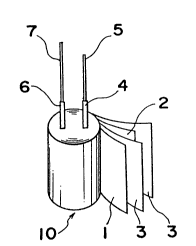
Fig. 2 shows the structure of a capacitor element 10 manu-
factured according to this method.
First, aluminum foils 1 and 2 of high purity (99.99~or more) are subjected to an etching step Sl for engraving
them electrochemically to increase their effective surface
areas. Next, oxide films la (thin films of aluminum oxide)
are formed on both surfaces of one aluminum film, by
treating it electrochemically in an electrolyte (electro-
chemical conversion treatment) in a second step S2. The
aluminum foil 1 having been subjected to the etching and
the electrochemical conversion treatment, is used as an
anode foil 1, while another film, having only been etched,
is used as a cathode foil 2 arranged opposed to the anode
foil 1, two sheets of manila paper 3 being put between the
foils 1 and 2 as a separator and on the outer surface of
the cathode foil 2. Stacked foils 1 and 2 and separators 3
are then wound cylindrically to form a capacitor element 10
in a winding step S3, as shown in Fig. 2. Reference
numerals 4, 6 and 5, 7 respectively designate aluminum
leads and lead wires, the leads 4, 6 being connected to the
foils 1, 2 after the electrochemical conversion treatment.
The capacitor element 10 thus formed is then subjected
to an impregnation treatment using a manganese nitrate
solution 8, as shown schematically in Fig. 3(a). The
portions of the manganese nitrate solution 8 on both sides
of the separators 3 are connected to each other through
,
08
the separators 3. The capacitor element 10 is then heated
in air to deposit manganese dioxide layers 9 of solid
electeolyte by thermally decomposing the manganese nitrate,
as shown schematically in Fig. 3(b). These impregnation
and thermal decomposition processes are repeated several
times to form dense manganese dioxide layers 9, in step s4.
The manganese dioxide layers 9 on both sides of the manila
paper separators 3 are connected to each other through such
separators. Further, graphite (carbon) powder dispersed in
manganese nitrate solution is impregnated into a space
between the manganese dioxide layer 9 and the cathode foil
2, and a carbon layer (not shown) is baked on the electro-
lytic layer. Next, in order to restore the thermal
deterioration of the oxide film caused by the thermal
decomposition used for forming the manganese dioxide layer
9, an electrochemical treatment in an electrolytic
solution, namely a reformation, is performed in a fifth
step S5. This reformation treatment enables the leakage
current to be decreased remarkably. A capacitor element
10 produced in this way is molded with resin, or is
installed in a metal case of aluminum or the like or in a
resin case, and is sealed with a sealant, such as an epoxy
resin, to complete the formation of a capacitor in a sixth
step S6.
In this capacitor, the separator 3 prevents mechanical
contact of the anode foil 1 with the cathode foil 2 and
separates these foils by a constant distance to prevent a
shor~ circuit between them and to guarantee a high voltage
breakdown. Further, it has been found that the thickness
of the separator 3 greatly affects the formation of the
manganese dioxide layer which largely plays the role of
cathode. The present invention is intended to improve the
impedance characteristic by setting the distance between
the foils 1 and 2 to be determined by the thickness oÇ the
separator 3.
-
.
. .
.
. .
., .
)8
Fig. 4 shows the frequency characteristic of theimpedance of aluminum solid electrolytic capacitors that
have been manufactured by the method described above to
have an electrostatic capacitance of 1 ~F and a rated
voltage of 16 V, as a function of the thickness of the
separator. In Fig. 4, curves 4A, 4B, 4C, 4D and 4E
correspond to capacitors having a separator thickness of
10, 30, 50, 60 and 100 ~m, respectively. As is apparent
from Fig. 4, the frequency characteristic of the impedance
improves with a decrease in the thickness of the separator.
The capacitor with a separator thickness of 100 ~m has a
too high an impedance to be used in practice, because it
is higher than 10 Q at 1 MHz. On the other hand, the
other capacitors with separator thicknesses up to 60 ~m
have impedances lower than lQ at 1 MHz, so that they are
suitable for practical use.
Fig. 5 shows the frequency characteristic of the ratio
of change in the electrostatic capacitance to that at 0.1
kHz of the capacitors having a capacitance of 1 ~F and a
rated voltage of 16 V, as a function of the thickness of
the separator, wherein curves 5A to 5E correspond to
capacitors having a separator thickness of 10, 30, 50, 60
and 100 ~m, respectively. As is apparent from Fig. 5, the
frequency characteristic of the ratio of change of capacit-
ance is better up to a higher frequency with smaller
separator thicknesses. For the capacitor with a separatorthickness of 100 ~m, the ratio of capacitance begins to
increase rapidly around 10 kHz, so that this capacitor is
hard to use in practice. On the other hand, the other
capacitors with a separator thickness up to 60 ~m have
curves of this ratio that increase comparatively gradually,
so that they can be used without any problem.
Fig. 6 shows the impedance characteristic of an
aluminum solid electrolytic capacitor manufactured
according to the first preferred embodiment of the present
invention, together with conventional capacitors for
~,''..
~28~0~3
--10--
comparison. In Fig. 6, the curve 6A denotes the impedance
characteristic of a capacitor according to the present
invention having a separator thickness of 30 ~m
(capacitance 10 ~F, rated voltage 16 V), while curves 6B,
6C and 6D respectively denote that of a conventional
tantalum capacitoe (capacitance 10 ~F, rated voltage 16 V),
a conventional aluminum solid electrolytic capacitor
(capacitance 10 ~F, rated voltage 16 V) and a conventional
solid electrolytic capacitor using a TCNQ salt as an
organic semiconductor (capacitance 10 ~F, rated voltage
25 V). It is apparent from Fig. 6 that the capacitor
according the invention, curve 6A, has a superior impedance
characteristic to the conventional tantalum capacitor and
aluminum solid electrolytic capacitor, especially at high
frequencies, and is as good as the solid electrolytic
capacitor that uses a TCNQ salt as an organic semiconductor.
Table 1 shows the relation between the thickness of the
separator and the measured defective ratio of short circuit
of aluminum solid electrolytic capacitors (capacitance 1 ~F,
rated voltage 16 V) made according to the first preferred
embodiment of the present invention. The number of samples
was fifth for each thickness.
The data compiled in Table 1 shows that the defective
ratio increases with a decrease in the thickness of the
separator and becomes as high as 8.26% at 5 ~m, while it is
lower than 1% at 10 ~m or more.
By taking into account the data shown in Figs. 4 to 6
and Table 1, it is preferred to set the thickness of
separator that determines the distance between the electro-
lytic foils at a value in the range between 10 and 60 ~m,preferably between 30 and 60 ~m.
, js .
8~
Table 1
.._
thickness of defective ratio
separator of short circuit
. _ .
100 ~m 0.20 %
0.20
._ .
0.21
0.32
.
0.90
8.26
..
As explained above, the impedance characteristic of an
aluminum solid electrolytic capacitor can be greatly
improved, especially at high frequencies, without
increasing the size thereof, so that it becomes applicable
to frequencies from 100 kHz to 10 MHz. Further, because
such a capacitor uses manganese dioxide the cost of which
is only about a hundredth of that of TCNQ salt, a capacitor
with a frequency characteristic as good a that of a conven-
tional solid electrolytic capacitor that uses an organic
semiconductor can be manufactured more cheaply.
,,~
,~ ,"
:
Fig. 7 shows a flow chart of a manufacturing method of
an aluminum solid electrolytic capacitor according to a
second preferred embodiment of the present invention, which
capacitor has improved impedance characteristic of
capacitance.
The capacitor element 10 is manufactured in the same
way as in the first preferred embodiment. Aluminum foils
of high purity (99.99% or more) are first subjected to an
etching treatment for engraving the foils electrochemically
to increase their effective surface area in a first step
Sll. Next, oxide films (thin films of aluminum oxide) la
are electrochemically formed on the surface of one of the
aluminum foils in the electrolytic solution (electro-
chemical conversion treatment) in a second step S12. The
aluminum foil 1, which has been subjected to both the
etching and the electrochemical conversion treatment, is
used as the anode, while another film 2, which has only
been etched, is used as the cathode arranged opposed to the
anode, and sheets 3 of manila paper as separators are put
between the foils 1 and 2 and on the foil 2, respectively.
The stacked foils 1 and 2 and the separators 3 are then
wound cylindrically, as shown in Fig. 2 to form the
capacitor element 10 in a third step S13.
The capacitor element 10 is then subjected to thermal
treatment to carbonize the manila paper to form separators
3' to lower the density by making the filaments thinner
(step S14). In this heat treatment, a temperature between
150 and 300C and a time of between 10 and 40 minutes are
suitable. By this treatment, the amount of manganese
nitrate to be impregnated into the capacitor element can be
increased and as a result the characteristics of the
capacitor can be improved.
The capacitor element 10 thus formed is then subjected
to impregnation treatment with a manganese nitrate
208
-13-
solution 8, as shown schematically in Fig. 8 (a). The
portions of the manganese dioxide solution 8 on both sides
of the separators 3' are connected to each other through
the separators 3'. The capacitor element 10 is then heated
in air to deposit manganese dioxide layers 9 of solid
electrolyte by thermally decomposing the manganese nitrate,
as shown schematically in Fig. 8(b). The manganese dioxide
layers 9 on the two sides of the separators are connected
to each other through such separators. This impregnation
and thermal decomposition step S15 is repeated several
times to form dense manganese dioxide layers 9. Further,
graphite (carbon) powder dispersed in a manganese nitrate
solution is impregnated into a space between the manganese
dioxide layer 9 and the cathode foil 2, and the carbon
layer ~not shown) is baked on the electrolytic layer.
Next, in order to restore the thermal deterioration of the
manganese dioxide layers 9 caused by the thermal decompo-
sition used for forming the manganese dioxide layer, an
electrochemical treatment in an electrolyte solution,
namely reformation, is performed at a sixth step S16.
~his reformation treatment enables the leakage current to
be reduced remarkably. An element 10 produced in this way
is molded with a resin, or is installed in a metal case of
aluminum or the like or in a resin case, and is sealed
with a sealant, such as an epoxy resin, to finish the
element as a capacitor (step S17).
In the manufacturing method the thermal decomposition
conditions of the manganese nitrate greatly affect the
formation of the manganese dioxide layer. If the tempera-
ture is too l.ow, the thermal decomposition of the manganesenitrate proceeds efficiently to invite a so-called "under-
decomposed" state, whereas if the temperature is too high,
the manganese nitrate is decomposed too much and this
invites a so-called "overdecomposed" state. In addition,
if the time for thermal decomposition is too short, the
manganese nitrate remains in the underdecomposed state,
,~ .
2 8 9
-14-
whereas if the time is too long, it enters the "overde-
composed" state. In either of such an underdecomposed or
overdecomposed state, the manganese dioxide layer will not
function efficiently as a solid electrolyte, so that the
S characteristics of the capacitor, such as tan ~ or the
impedance, are deteriorated.
Table 2 shows the relation between the conditions of
thermal decomposition and the characteristics of an
aluminum solid electrolytic capacitor having a capacitance
of 10 ~F and rated voltage of 16 V. The number of samples
was fifth for each test. The temperature was varied within
a range between 180 and 280C and the decomposition time
was varied within a range between 10 and 50 minutes. In
Table 2, tan ~ and impedance denote values measured at 1
kHz and at 100 kHz, respectively. The evaluation is
derived from both tan ~ and the impedance together, that
is, the evaluation is good (O) if tan ~ is less than 0.04
and the impedance is less than 0.4 Q, not so good (~) if
tan ~ is between 0.4 and 0.5 Q, and bad (x) if tan ~ is
0.051 or more and the impedance is 0.51 Q or more. It was
found that a decomposition temperature between 200 and
260C and a decomposition time between 20 and 40 minutes
are optimum.
-15 ~ 1`2892~
Table 2
. . _ _ .
temp (C) time (min) tan 6 impedance (n) Evaluation
.. .. _ _
180 10 0.091 1.18
180 20 0.083 0.96
180 30 0.079 0.84 X
180 40 0.073 0.84 X
180 50 0.070 0.82 X
200 10 0.071 0.84 X
200 20 0.046 0.49
~00 30 0.042 0.48 ~
200 40 0.038 0.45 o
-
200 50 0.049 0-53
. _ _
220 10 0.065 0.76 X
220 20 0.043 0.48 ~
.. _ _ . .. . . . _
220 30 0.036 0.39 o
220 40 0.030 0.33 O
220 S0 0.051 0.57 X
.
240 10 0.053 0.63
-
240 20 0.037 0.39 O
. . _ _ _
240 30 0.023 0.29 O
240 40 0.025 0.30 O
240 S0 0.054 0.58 X
260 10 0.053 0.61 X
260 20 0.030 0.32 O
_ _ _ _
260 30 0.032 0.35
260 40 0.040 0.40
260 50 0.050 0.67
_ _ _ _ _
280 10 0.053 0.62 X
-
280 20 0.057 0.67 X
280 30 0.061 0.70
. .
280 40 0.064 0.79 X
280 50 0.072 0.91 X
128~08
--16--
Fig. 9 shows the frequency characteristic of impedance
obtained under various decomposition conditions. Curves 9A,
9B and 9C correspond to conditions of 180C, 30 minutes;
280C, 30 minutes and 240c, 30 minutes, respectively. The
last conditions of 240C and 30 minutes give an excellent
impedance characteristic.
Fig. 10 shows a flow chart for a manufacturing method
according to a third preferred embodiment of the present
invention.
As is apparent from a comparison of Fig. 10 with Fig. 7,
the only difference is that the manganese nitrate solution
with a fine powder of manganese dioxide (MnO2) is used for
impregnation (step S25).
Namely, in the third preferred embodiment, a fine powder
of manganese dioxide is added beforehand to the manganese
nitrate solution, although manganese dioxide itself is
formed by the thermal decomposition of the manganese
nitrate. The amount of added fine powder of manganese
dioxide greatly affects the formation of the manganese
dioxide layer.
The other steps S21-S24 and S26-S28 corresponds to the
steps Sll-S17, respectively (Fig. 7).
Table 3 shows the relation between the amount (weight
percent) of fine powder of manganese dioxide and the
impedance of 100 kHz, wherein fifty capacitors of rated
voltage 16 V and capacitance 10 ~F were measured for each
amount of addition between 0 and 10% in steps of 2%.
The eesult shown in Table 3 suggests that an amount of
addition between about 4 and 6 wt% is the most favorable
for the impedance chaeacteristic.
Fig. 11 shows the relation of the frequency character-
istic of impedance with the amount of addition of manganese
diox$de powder, wherein curves llA, 11~, llC, 11D, llE and
llF correspond respectively to amounts of addition of 0, 2
4, 6, 8 and 10%.
, ,
39~08
-17-
Table 3
. __ . _
amount of
MnO2 added impedance (at 100k~z)
0 % 0.46 n
. .'
2 % 0.48 n
. ._
4 % 0.30 n
. . ~
6 % 0.26 n
8 % 0.46 n
. _
10 % ¦ 0.54 n
I
Fig. 11 also suggests that the amount of the addition
of the fine powder of manganese dioxide is best in the range
between about 4 and 6 wt%.
By using a fine powder of manganese dioxide of about 4
to 6 wt%, the frequency characteristic of an aluminum solid
electrolytic capacitor can be improved, especially at high
frequencies, without enlarging its size. Further, this
process is favorable for lowering the cost, because no new
steps; are required, and it can be adopted for practical use.
Fig. 12 shows a flow chart for a manufacturing method of
a capacitor according to a fourth preferred embodiment of
the present invention.
The fourth preferred embodiment is characterized in that
a lithium doping step S36 is performed after the thermal
decomposition of the manganese nitrate impregnated into the
capacitor element. A carbon layer is then baked in a space
between the manganese dioxide layer 9 and the cathode foil 2
(step S37). Other steps S31-S34, S38 and S39 are substan-
tially the same to those Sll-S14, S16 and S17 of the second
preferred embodiment (Fig. 7).
:~: 4".
,~ .
o~
-18-
In step S36, the capacitor element 10 in which the
manganese dioxide layer has been formed is immersed as an
active electrode together with a lithium plate as a counter
electrode in a mixed electrolytic solution of lithium
chlorate, propylene carbonate and dimethyl ether, and a
constant current of 0.1 to 0.3 mA per element is applied in
the electrolytic solution. During this process, Li+ ions
in the electrolytic solution diffuse into the crystal
lattice of manganese dioxide (MnO2) in the solid state,
so as to cause the following reaction to reduce quadrivalent
Mn to trivalent Mn:
Li + Mn ~IV) 2 + ~n (III) O (Li
Further, a carbon layer is baked on the electrolytic
layer in step S37.
The lithium doping after the formation of the manganese
dioxide layers 9 in the manufacture of a capacitor enhances
the electrical conductivity of the manganese dioxide layers
and improves the characteristics of the capacitor.
Table 4 shows differences in the characteristics between
capacitors manufactured with and without using tbe lithium
doping process. The impedance at 100 kHz and tan ~ at 120
kHz were measured for fifty samples of each capacitor having
a rated voltage of 16 V and a capacitance of 10 ~F, and
respective averages being calculated from the measured
valuies.
Table 4
lithium
impedance (lOOkHz) tan 6 (120Hz)
doping
none0.46 n 2.6 %
doping 0.21 n 1.8 ~
08
--19--
As is clear from Table 4, both of the impedance and the
tan ~ of the capacitor in which lithium was doped are
improved remarkably relative to one without doped lithium.
Fig. 13 shows the frequency characteristic of impedance
of a capacitor manufactured using lithium doping (13A~ and
of a capacitor manufactured without using lithium doping
(13B). Fig. 13 clearly indicates that the impedance charac-
teristic is greatly improved, especially at high frequen-
cies, when using the lithium dopin~ process.
Fig. 14 shows a flow chart for a manufacturing method of
a capacitor according to a fifth preferred embodiment of the
present invention.
A capacitor element 10 as shown in Fig. 2 is manufac-
tured through the first to third step S41 to S43 similar to
those of the foregoing preferred embodiments.
Next, any scratches on the aluminum foils or defects in
the foils caused at their cut edges or the like are restored
with an electrochemical conversion treatment in a weak
acidic electrolytic solution (cut edge reformation) in a
fourth step S44.
The element 10 is then subjected to thermal treatment
to carbonize the manila papers to form the separators 3' and
lower the density by making the filaments thinner in a fifth
step S4S, under conditions of a temperature between 150 and
300C and a time between 10 and 40 minutes.
The element 10 is then subjected to an electrochemical
conversion treatment (step S46) to restore the oxide film
which has been deteriorated thermally.
The element 10 thus formed is then subjected to impreg-
nation with the manganese nitrate solution. Then, the
element 10 is heated in air under conditions, for example,of a temperature between 200 and 260C and a time between
20 and 40 minutes, whereby to decompose thermally the
impregnated manganese nitrate to deposit a manganese dioxide
layer of solid electrolyte (step S47). The impregnation
and thermal decomposition processes are repeated several
, . .
'': .
~;~8~t~08
-20-
times to form dense manganese dioxide layers similarly to
the foregoing preferred embodiment. During this manganese
dioxide formation process or before completion of the forma-
tion of the solid electrolyte of manganese dioxide, a
S further electrochemical conversion treatment (mid-formation)
(step S48) is performed through the solid electrolytic layer
similarly to the electrochemical conversion treatment of
step S42. The thermal deterioration of the oxide film
caused by thermal decomposition is thus restored.
Next, another thermal decomposition treatment (step S49)
is performed using manganese nitrate wherein graphite
(carbon) powder has been added under conditions substan-
tially the same as those of the above-mentioned thermal
decomposition, whereby to perfect the formation of the solid
electrolytic layers 9 of manganese dioxide (manganese
nitrate thermal decomposition). Further, graphite ~carbon)
powder in an amount much laeger than that used in the
manganese nitrate thermal decomposition process, dispersed
in the manganese nitrate solution, is impregnated into the
space between the solid electrolytic layer 9 and the cathode
foil 2, and a carbon layer is formed on the solid electro-
lyte by baking the carbon under conditions substantially the
same as in the above-mentioned thermal decomposition condi-
tions (carbon layer baking) (step S49). The carbon layer
fills the space between the solid electrolyte 9 and the
cathode foil 2, so that the contact resistance between them
is decreased and the layer 9 is protected.
Next, in order to restore the thermal deterioration of
the oxide film caused by the foregoing carbon layer baking
(step S49), an electrochemical treatment in an electrolytic
solution, namely reformation, is performed (step S50).
The capacitor element 10 thus manufactured is molded
with resin (resin dip), or is sealed with epoxy resin or
the like after being inserted into a metallic case of
~i:
,,
aluminum or the like or into a resin case (case inseetion
or resin sealing) (step SSl) to form a finished capacitor.
Table S shows the relation between the leakage current
and the defective ratio of short circuits of various
combinations of the cut edge formation (step S44), mid-
formation (step S48) and reformation (step S49), wherein O
and X denote the adoption and the non-adoption of each
step, respectively. All of the samples used for measurement
had a eated voltage of 16 V and a capacitance of 10 ~F.
, :
.:
. - '.
31208
~o __ ~ _ ~ o ~ o
~ o o co O ~ O ~1
~o~ - I~
~
.'~ O O X X O O X X
~I G ~
.
'-`
lZ8~
--21--
The leakage current shows an average o~ fifty samples,
while the defective ratio of short circuits denotes a ratio
of the samples having a large leakage current (of an order
of nA) to 100 samples.
Table 5 shows clearly that both of leakage current and
the short circuit ratio are most improved when all the cut
edge reformation, mid-formation and reformation processes
are performed (No. 5). The comparison of cases of No. 5 and
No. 7 makes the effect by the mid-formation process clear.
In this preferred embodiment, because the mid-formation
treatment (step S48) is performed before the carbon baking
treatment and before forming a solid electrolytic layer
(step S49), the oxide film deteriorated in the thermal
decomposition step S47 can be restored completely without
suppressing the electrochemical conversion with the solid
electrolyte and carbon layers.
Although manufacturing methods for a capacitor of the
winding type have been explained in the foregoing preferred
embodiments, the present invention is also applicable to a
chip capacitor (surface mount type of capacitor), as will
now be explained~
Figs. 15(a) and 15(b) shows a chip capacitor, namely a
cylindrical capacitor 20 with a cylindrical case 21 wherein
a capacitor element manufactured according to the present
invention is installed. A small rectangular sheet 22 is
fixed on the cylindrical surface 20a of the capacitor 20.
The 8heet 22 is made of a fluorine-contained resin, silicone
resin, polyimide resin or the like, of a size of about 4 mm
x 5 ~m with a thickness 0.2 mm, and it is bonded on the
surface 20a with a heat resistant binder, such as an epoxy
resin or W resin, or with a pressure sensitive adhesive
double coated tape. Any binder can be used if its position
does not move at room temperature and it does not peel on
reflow of solder.
:;:
f,,
"( ';.'
2~8
-24-
The cylindrical capacitor 20 with the sheet 22 can be
used as a chip capacitor which can be set in the horizontal
direction.
The chip capacitor 20 can be mounted stably on a printed
circuit board. Further, the heat resistant sheet 22 can
protect the main body of the capacitor 20 from the heat of
the circuit board on soldering. Leads 23 can be bent
properly for use as a chip capacitor.
Fig. 16 shows a similar type of chip capacitor 20 with
a sheet 24 which has a curved inner face along the side 20a.
Such a sheet can be produced, for example, by a formation
process. The sheet 24 makes it stable to locate the capa-
citor on the printed circuit board, and prevents possible
cracking of the casing tube of the capacitor and deteriora-
tion of its characteristics due to heat transmitted from the
circuit board.
Figs 17(a) and 17(b) show a chip capacitor e~uipped witha first sheet 25 for fixing the capacitor 20 stably on a
printed circuit board and a second sheet 26 for serving as
a plane for engagement when mounting the capacitor on a
printed circuit board using an absorbing chuck. The second
sheet 26 has a similar size and thickness of about 0.2 to
0.3 mm as the first one 25, and is adhered to the capacitor
20 with, for example, a quick-drying epoxy resin. By
forming a plane for engagement, the absorbing chuck need not
necessarily have an engagement surface adapted to the curved
surface of the chip capacitor. As a result, no special
chuck is needed, but an ordinary one can be used for
mounting the chip capacitor, and it is not necessary to dis-
criminate between the top and bottom thereof. The second
sheet 26 is preferably made of a polyvinyl chloride resin,polyimide resin, fluorine-contained resin or the like.
Figs. 18(a) and 18(b) show a chip capacitor similar to
- that shown in Figs. 17(a) and 17(b), except that a second
sheet 28 has a curved face adjacent the periphery 20a of
,
:
-25-
the capacitor 20. A second sheet 28 with such a curved face
can be obtained, for example, by a forming process.
Figs. l9(a) and l9(b) show a capacitor 20 similar to
that shown in Figs. 17(a) and 17(b), except that a spacer 29
having an upper plane 29a and a lower plane 29b is employed
instead of using the two sheets 25, 26. This capacitor 20
can be put on a printed circuit board on the plane 29a, while
the other plane 29b serves as an engaging plane. Because the
capacitor 20 has upper and lower planes, it can be mounted
using an ordinary chip mounter, in the same way as an ordi-
nary chip capacitor having rectangular cross-section.
Figs. 20(a) and 20(b) show a capacitor 20 having a sheet
31 of a roughly square shape adhered to an end face 20b of
the capacitor 20. The sheet 31 is fixed offset from the axis
of the capacitor 20, so that the sheet 31 and bent leads 23
can support the main body of the capacitor 20 a little above
the surface of a printed circuit board. Thus, the capacitor
20 can be fixed firmly on the circuit board with a gap there-
between, by adhering the lower portion of the sheet 31
thereon.
In the sealing process in the manufacturing method for an
aluminum foil type of solid electrolytic capacitor, such as
steps S6, S28, S39 or S51 in Figs. l, 10, 12 or 14, a capa-
citor element such as shown in Fig. 2 is inserted into a case
and is sealed with resin. If the filling with resin makes
the position of the capacitor element deviate from the
centre, defects such as a short circuit are liable to happen.
It is thus necessary to fix the capacitor element in the case
temporarily for sealing with resin. In the sealing process,
a small amount of thermoplastic resin is placed in the case
and is melted by heating. After the capacitor element has
been installed in the case, the resin is cooled to fix the
capacitor element therein. Thermoplastic resin is then
- inserted to fill the case for sealing.
,,~
~.;
.
~g~
However, this sealing step has the following problems.
First, it does not take into account the moisture resistance
of resin for temporary fixing. Therefore, water is liable
to penetrate the contact boundary between the resin layer
and either the case or the leads and be absorbed into the
capacitor element. Because water acts as an electrolyte,
the electrostatic capacitance is thus increased. Further,
two kinds of resin are needed for temporary fixing and for
sealing.
A capacitor element 40 manufactured according to any one
of the foregoing preferred embodiments is installed in a
case 41 of metal, such as aluminum, or of resin, as shown in
Fig. 21. Thermosetting resin 42 has been put in the case 41
beforehand to fill about ten percent of the inner volume of
the case 41. After the capacitor 40 has been installed in
the case 41, it is heated for hardening the resin 42, for
example, at a temperature of 80-90C for ten minutes, so
that the capacitor element 40 is fixed temporarily in the
case 41. The case 41 is then filled up to its mouth 44 with
thermosetting resin 43 which is of the same kind as the
thermosetting resin 42. Next, the case 41 is heated for
hardening, for example, at a temperature of 50 to 110C for
a time between six and ten hours.
The heating temperature of the resin 43 for sealing the
mouth 44 of the case 41 should desirably be as low as
possLble in order to make it easy to remove resin adhered
to the leads 46, 47 in the subsequent rinse process.
~ s explained above, the same thermosetting resin is used
both for fixing the capacitor element in the case and for
sealing the opening of the case in which the capacitor
element has been fixed. Therefore, water can be intercepted
so as not to penetrate into the capacitor element 40 from
the exterior, so that any enhancement of the electrostatic
capacitance can be prevented, since the capacitor element
does not absorb water. Further, since the same resin is
used for temporary fixing and for sealing, the manufacturing
. ~
-27-
steps can be shortened.
Conventionally, such a chip capacitor is manufactured by
deforming leads of an aluminum solid electrolytic capacitor,
welding the leads to metallic terminal plates and molding
the capacitor and the welded parts with resin. However,
such a welding step requires complicated work in which the
efficiency and productivity are low. Further, the resin
molding step requires large-scale apparatus which is
expensive.
Figs. 22 and 23 show examples of a chip capacitor
according to the present invention which can solve the
above-mentioned problems. Capacitor elements 60, 70 are
manufactured as a capacitor element 10 as explained above.
The leads 61 and 62 are arranged on the same side of the
element 60 in the case of Fig. 22, while the leads 71 and 72
are arranged on different ends of the element 70 in the con-
necting step to the aluminum foils in the case of Fig. 23.
In the case of Fig. 22, one lead 61 is cut shorter than
the height of the metallic case 63 which contains the ca2a-
citor element. Liquid epoxy resin 64 of good moistureresistance is put on the bottom of the metallic case 63.
Next, the capacitor element 60 is inserted into the metallic
case 63 and is bonded with the resin to the metallic case 63
with a thermal setting process. Then, the shorter lead 61
and the inside of the metallic case 63 are bonded with a
conductive adhesive 65 of high heat resistance of 270C or
more. Then, the opening of the metallic case 63 is poured
with,the same liquid epoxy resin 66 of good moisture resist-
ance as used for the bonding, and the resin 66 is hardened
thermally for sealing. The lead 62 passing through the
sealing material 66 is formed beforehand like a plate
insulated from the case by an insulating member 67.
In the case of Fig. 23, a shorter lead 71 is formed as
an "Ln. Solder 74 having a melting point of 270C or more
is melted in the bottom of the metallic case 73. The
capacitor element 70 is then inserted into the case 73 so
; ,~,
""~
1~8g20f~
-28-
that the lead 71 is bonded to the case 73 with solder 74.
Next, the opening of the case 73 is sealed with epoxy resin
75 of good moisture resistance which is the same as used in
the above-mentioned chip capacitor of Fig. 22. Then, the
other lead 72 which penetrates the sealant material 75 is
formed like a plate as a metallic terminal plate insulated
from the case 73 by an insulating element 76.
Figs. 24 and 25 show modified examples wherein metallic
terminal plates 68 and 77 are bonded to the metallic cases
63 and 73 by welding or the like and are fixed on insulating
material 67' and 76' at the bottom before inserting the
capacitor element 60, 70 into the metallic case 63, 73.
Both plates 62, 68 and 72, 77 can be set in the same plane.
In the examples of this embodiment, one of the leads of
a capacitor element is bonded with a metallic case so that
the metallic case can be used as an extension of the
electrode. Thus, resin molding is not necessary, and cheap
and compact chip type capacitors can be provided.
This invention may be embodied in still other ways
without departing from the spirit of the essential
characters thereof. The preferred embodiments described
herein are therefore illustrative and not restrictive, the
scope of the invention being indicated by the appended
claims and all variations which come within the meaning of
the claims are intended to be embraced herein.