Note: Descriptions are shown in the official language in which they were submitted.
~89232
FIELD OF THE INVENTION
This invention relates generally to solar
cells and more particularly to thin film photovoltaic
structures formed from either one or a plurality of
stacked solar cells electrically and optically
interconnected in series. The intrinsic layer of at
least one of said plurality of solar cells is
"spatially graded" through a substantial portion of
the bulk thickness thereof, which portion is removed
from the intrinsic layer-dopant layer interfaces for
enhancing the open circuit voltage and/or the fill
factor.
BACKGROUND OF THE INVENTION
It is to be noted that the assignee of the
instant invention has achieved the highest reported
thin film solar cell photoconversion efficiency, an
efficiency of about thirteen percent. This record was
achieved utilizing a photovoltaic structure in ~hich
three discrete p-i-n type solar cells were optically
and electrically stacked in series, each cell
dedicated to the absorption of photons of incident
radiation of a particular portion of the solar
spectrum. Through this "spectrum splitting"
technique, it becomes possible to fabricate the
stacked photovoltaic structure with a plurality of
., ~P
~ ~.
So-241 128~232
relatively thin photogenerative layers so that the
built-in electric field provided by the doped layers
effectively collect photogenerated charge carriers and
thereby minimize recombinative losses due to
"Staebler/Wronski" degradation. The manner in which
stacked cells operate to minimize recombinative losses
will be described in greater detail in a later portion
of this Background.
The concept of utilizing multiple stacked
cells to enhance photovoltaic device efficiency was
described as early as 1955. The multiple cell
structures disclosed in 1955 were limited to the
utilization of p-n junctions formed by single
crystalline semiconductor devices. Essentially, the
stacked cell concept employs different bandgap devices
to more efficiently collect various portions of the
solar spectrum and to increase VOC (open circuit
voltage). In the uppermost or light incident cell, a
relatively large bandgap semiconductor material
absorbs only the short, highly energetic wavelength
light; while in the subsequent cells, subsequently
smaller bandgap materials absorb the longer, less
energetic wavelengths of light which pass through the
first cell. By substantially matching the
photogenerated currents from each serially connected
cell, the overall open circuit voltage becomes the sum
of the open circuit voltage of each cell; while the
short circuit current (Jsc) of each cell remains
substantially constant. Such tandem structures are
now commercially employed by the assignee of the
instant invention in the large area photovoltaic
devices referred to hereinabove by utilizing the
aforementioned continuous processing techniques for
depositing successive thin film layers of amorphous
and microcrystalline semiconductor alloy materials.
S0-241 ~2~9232
In the description which follows, it is to be
kept in mind that specialized definitions of
amorphicity and microcrystallinity are employed. The
term "amorphous", as used herein, is defined to
include alloys or materials exhibiting long range
disorder, although those alloys or materials may
exhibit short or intermediate range order or even
contain crystalline inclusions. The term
"microcrystalline", as used herein, is defined as a
unique class of said amorphous materials characterized
by a volume fraction of crystalline inclusions, said
volume fraction being greater than a threshold value
at which the onset of substantial changes in certain
key parameters such as electrical conductivity,
optical bandgap and absorption constant occurs. It is
to be specifically noted that pursuant to the
foregoing definitions, microcrystalline material falls
within the generic class of amorphous materials.
The assignee of the instant invention has
also been active in the development of (1) improved
semiconductor alloy materials, both wide and more
narrow bandgap materials, which materials are
characterized by a reduced density of defect states
(as low as about 1016cm 3eV 3); (2) improved
back reflector materials, including dual layer, highly
reflective materials (such as silver buffered by a
layer of zinc oxide); and (3) improved, wide bandgap
doped layers of semiconductor alloy material
characterized by high conductivity for increasing the
built-in electric field of the solar cells in which
they are incorporated. All of these developments were
essential in order to develop the aforementioned
triple stacked photovoltaic device exhibiting the
world record 13~ photoconversion efficiency. However,
as described hereinabove, even that world record
S0-241 ~28~232
efficiency remains insufficient to provide for cost
effective competition between photovoltaically
generated electricity and electricity derived from
more conventional, depletable energy sources.
It was in an effort to further increase the
photovoltaic conversion efficiency of solar cells that
the development work which led to the improved cell
performance occasioned by the instant invention was
undertaken. The strategy employed by the instant
inventors was to return to basic considerations which
impact upon thin film solar cell design, which
considerations are currently accepted by researchers
in the field and to reexamine the "conventional
wisdom" or given truths regarding the operational
interactions of the multilayers thereof. Said
inventors were particularly interested in examining
the physics of operation of the intrinsic layer of
semiconductor alloy material of single and tandem
solar cells so as to find a means for enhancing the
open circuit voltage derived therefrom without
sacrificing the efficient collection of photogenerated
charge carriers. It should be noted as a base-line
reference, that photovoltaic design had heretofore
required the presence of a homogeneous thin film layer
of amorphous silicon alloy material (for 1.7eV optical
bandgap material) or amorphous silicon germanium alloy
material (for less than 1.7eV optical bandgap
material) sandwiched between layers of p and n-type
semiconductor alloy material. Prior to summarizing
the inventive concept disclosed herein, it will be
helpful to detail the efforts of researchers in the
field to improve solar cell efficiency by modifying
the homogeneous nature of the intrinsic layer of
~. :
semiconductor alloy material represented by said
"base-line."
~;
.
~ ~ .-, .- -,. . , .. '
-
i - . ,. ; .. :, . : . .
. , : , .. .
.
- .
~289232
In the course of this analysis, the instant
inventors revisited the work of others in the field of
solar cell fabrication to consider the type of
"unusual" intrinsic layer designs which had previously
been considered. For instance, a photovoltaic device
constructed with a varying bandgap in a narrow portion
of the intrinsic layer is disclosed in a paper
entitled "Achievement of Higher Efficiency Amorphous
Silicon-Germanium Solar Cells Using Affinity
Gradients" presented by S. Wiedeman and E. A. Fagen at
the 17th Annual I.E.E.E. Photovoltaic Conference held
May 1-4, 1984 in Kissimmee, Florida. Disclosed
therein is a n-i-p-type photovoltaic device formed of
an amorphous silicon-germanium alloy in which the
composition of the intrinsic layer of semiconductor
alloy material was profiled over the first few hundred
angstroms from the light incident surface thereof.
This bandgap variation was accomplished by gradually
altering the ratio of silicon to germanium in those
few hundred angstroms. The object of such bandgap
variation was to establish an electrical field of
varying strength adjacent the light incident surface
of the intrinsic layer of semiconductor alloy
material, which field was adapted to decrease if not
eliminate charge carrier losses at the interface of
; the n type and intrinsic layer. Such losses were
occasioned by the back diffusion of charge carriers
across the n layer and intrinsic layer interface. The
authors of the paper claimed that, because of the
presence of the electric field, a 29% improvement in
the initial photoconversion efficiency of the
photovoltaic devices was achieved.
In commonly assigned U.S. patent No.
3,547,621 entitled "Stable Photovoltaic Devices And
Method of Producing Same"
: : : ' , .:
~ ;
.
-
1289232
--6--
M. Hack and S. Guhagraded the bandgap of the intrinsic layer of silicon
alloy material of a light incident n-i-p type
photovoltaic device such that the wider bandgap
portion was disposed proximate the light incident
surface. The wide bandgap portion (a) was formed so
as to be less than one half the thickness of the
remaining narrower bandgap portion and (b) included at
least one bandgap broadening element not present in
the narrower bandgap portion. In this manner, the
authors attempted to provide for the uniform
absorption of photons of short, highly energetic
incident radiation throughout at least a substantial
portion of the bulk of the intrinsic layer so as to
promote the photogeneration of electron-hole pairs
throughout said substantial portion of the intrinsic
layer and thereby reduce charge carrier recombination
therein. In this manner, the authors claimed to
improve long term stability.
In commonly assigned U.S. patent No.
4,379,943 entitled "Current Enhanced Photovoltaic
Device"
C. Yang, A. Madan. S. Ovshinsky
and D. Adler disclosed the fabrication of a novel
photovoltaic structure in which the intrinsic layer of
semiconductor alloy material includes a first
intrinsic layer formed of a non-etching
(non-fluorinated) precursor gaseous mixture and a
second intrinsic layer preferably formed of silicon
and fluorine. The thicknesses of the first and second
intrinsic layers were adjusted to match the respective
potential drops thereof with the first intrinsic layer
being relatively thin and the second intrinsic layer
being relatively thick. The short circuit current of
the photovoltaic device was said to be enhanced
: . .
'' ' ~, - ' :
-:' , ' .`-~ ~ , ' `
.,
' ~
~289Z32
because the first and the second intrinsic layers are
fabricated with differing bandgaps so as to provide a
field throughout those layers.
In commonly assigned U.S. patent No.
4,471,155 entitled "Narrow Band Gap Photovoltaic
Devices With Enhanced Open Circuit Voltage"
R. Mohr and V. Cannella designed a
photovoltaic device which provided enhanced open
circuit voltage by fabricating the narrow bandgap
intrinsic semiconductor alloy material thereof so as
to include a second intrinsic region having a bandgap
wider than the bandgap of the first intrinsic region.
The second bandgap region is disposed between the
first bandgap region and one of the doped layers.
This open circuit enhancement structure can also
include a third intrinsic region, which region has a
wider bandgap than the first intrinsic region and is
disposed on the side of the first intrinsic region
opposite the second intrinsic region. As is
explicitly stated in paragraph 3, lines 18-26 of this
patent, "One effect of the increased density of defect
states in amorphous silicon-germanium alloys is the
reduction in open circuit voltage by an amount larger
than can be reasonably expected by the reduction in
band gap. This reduction in voltage is attributed to
increased recombination at the increased defect
states, and to interface states introduced by bandgap
and structural mismatch at the doped region-intrinsic
region boundary." (The emphasis was added because the
underlined quote inferentially indicates that prior to
the instant invention, it was commonly accepted that
open circuit voltage delivered by a given cell was
limited by the bandgap of that cell).
The review of thin film solar cell design
S'~
:
- : :,
S0-241
128923Z
undertaken by the instant inventors also located
patents which disclosed solar cells wherein the
intrinsic layers of semiconductor alloy material were
graded substantially throughout the bulk thickness
thereof. Specifically relevant were two patents of S.
Yamazaki; the first being U.S. patent No. 4,239,554
entitled "Semicondùctor Photoelectric Conversion
Device" and the second being U.S. patent No. 4,254,429
entitled "Hetero Junction Semiconductor Devices." It
is to be noted that the disclosure of the Yamazaki
patents ascribe the inventor's motivation in grading
the intrinsic layer was to eliminate the notch or
spike which can be formed at the heterojunction
(defined, for purposes of this description, as the
junction between two regions of the intrinsic material
characterized by different bandgaps), said spike being
due to the absorption of holes or electrons moving
from one of two adjacent semiconductor regions across
the heterojunction and into the other region. It is
to be noted, however, that the reason for such
gradation in the Yamazaki patents was to provide for
charge carrier transport from the wide bandgap energy
of one of the doped layers to the narrow bandgap
energy of the oppositely doped layer without
interposing a spike which would prevent or at least
interfere with charge carrier mobility. Thus,
Yamazaki noted that such transport could most easily
: be affected by a smooth, continuous bandgap variation
through the intrinsic layer.
With this analysis of the prior art in
intrinsic layer design as a backdrop and once again
: : realiz-ing that a multijunction approach to the
; development of high efficiency and stable amorphous
silicon alloy solar cells will yield the best results;
the critical solar cell design considerations for the
- ,'' :. ' ,
. .
.. . :-. -
S0-241 i289232
g
fabrication of intrinsic layers of single as well as
for tandem photovoltaic structures can now be
enumerated. In this approach, the intrinsic layer of
each discrete cell is relatively thin so that the
photogenerated charge carriers have a relatively short
distance to travel before reaching the respective
electrodes thereof. At the same time, by stacking a
plurality of cells in optical and electrical series
relation, all of the photons of the incident solar
spectrum are absorbed with discrete cells dedicated to
the absorption of a particular range of wavelengths.
Since the current photogenerated by each cell must be
matched, the top cell is made thin and therefore
exhibits stability against the degrading effects of
light exposure. The lower cells receive progressively
less intense illumination and due to the fact that a
cell receiving light of less intensity over a longer
period of time does not degrade as much as a cell
receiving light of greater intensity over a shorter
period of time; the lower cells can be made
progressively thicker without jeopordizing stability.
The p-type and n-type layers provide the
internal electric field across the intrinsic
(photogenerative) layer of a solar cell. It is
important that the doped layers are characterized by
the highest possible conductivity so that there is no
rectifying internal junction formed between the p and
n layers of contiguous cells. Further, and of equal
importance, high conductivity p and n layers increase
the built-in electric field across the photogenerative
intrinsic layer, thereby increasing the open circuit
voltage and fill factor of the cell. It is of
substantial importance that the p and n layers be
fabricated of wide band semiconductor alloy materials
(certainly wider than the bandgaps of the intrinsic
:
.
:' ' ' , :
, ~ ~ ' . -
;~ '
', ' ' '
SO-241 ~289232
--1 o--
layers) so as to exhibit little or no optical
absorption of photogenerative photons of incident
radiation (charge carriers generated in the doped
layers will instantaneously recombine).
It is additionally necessary that the narrow
bandgap semiconductor alloy material be of as high a
quality (possess as low a density of defect states~ as
possible. Of course, as the bandgap of the amorphous
silicon alloy material is lowered through the addition
of tin, or preferably germanium, additional defect
states are created. This is due to (1) the
preferential attachment of hydrogen atoms to silicon,
thereby creating dangling bonds of germanium in the
alloy; (2) the tendency of germanium to assume
divalent configurations, thereby initiating additional
defect states; and (3) the tendency of non-crystalline
germanium films to grow in a columnar fashion, thereby
degrading film quality. As previously mentioned, the
assignee of the instant invention has, through the
incorporation of fluorine into the narrow bandgap
material, effectively lowered the density of defect
states ana the degree of sub-bandgap absorption in the
material without changing the slope of the valence
band tail as the optical bandgap is decreased to a
value as low as about 1.25eV.
SUMMARY OF THE INVENTION
In the Examples which follow hereinafter, the
instant inventors have demonstrated the manner in
which the intrinsic layers of thin film amorphous
silicon alloy solar cells have been specially designed
so as to significantly enhance open circuit voltage
without deleteriously effecting the collection of
photogenerated charge carriers. The solar cell
S0-241
i289232
designs disclosed below begin by discarding the
conventionally accepted axiom that the maximum open
circuit voltage which can be delivered by a single,
but multigapped, solar cell is determined by the width
of the most narrow portion of the bandgap of the
intrinsic layer thereof. While the rationale for such
a belief is evident, namely that the available voltage
is limited to the degree which the quasi fermi level
of the intrinsic layer of semiconductor alloy material
splits, upon illuminationi the instant set of
experiments conclusively prove that no such limitation
exist. Rather, it is speculated herein that the
amount of open circuit voltage which can be obtained
is limited by the degree which the quasi Fermi level
of the widest bandgap portion of the intrinsic layer
of semiconductor alloy material splits. This finding
is not only significant because of the immediate
improvement in open circuit voltage which has been
demonstrated, but also because of the myriad of novel
design considerations and novel structures which can
be explored. For example, it is known, as mentioned
above, that as the bandgap of semiconductor alloy
material decreases, the quality of that material also
deteriorates. However, spectrum splitting
photovoltaic structures require the use of narrow
bandgap silicon germanium alloy material even though
charge carrier collection in such material is limited
by the increased density of defect states present
therein`. More specifically stated, a good fill factor
requires a long diffusion length, which diffusion
length is shortened by the added density of defect
~; states in narrow bandgap silicon germanium alloy
material. Therefore, researchers found themselves
locked in a stalemate in an effort to develop a solar
cell characterized by the highest combination of
~; :
~,
:
.
~ .
:~ ~
S0-241 1~89232
efficiency and stability; in order to collect the
maximum number of incident photons, low bandgap
material must be used, however, the efficiency of
collection decreases with the use of such narrow
bandgap material.
The invention disclosed herein affords said
researchers a method of unblocking that stalemate by
making use of novel graded bandgap intrinsic layer
structures. Such structures may take any one of three
basic formats. In the first of these formats, the
intrinsic layer is structured so that the widest
bandgap region of silicon alloy material is disposed
at the p-type layer interface and graded therefrom
throughout a substantial portion of the bulk to the
most narrow bandgap region of silicon germanium alloy
material adjacent the n-type layer interface. In the
second of these formats, the intrinsic layer is
structured so that the narrowmost bandgap region of
silicon germanium alloy material is disposed at the
p-type layer interface and graded therefrom throughout
a substantial portion of the bulk to the widest
bandgap region of silicon alloy material adjacent the
n-type layer interface. In the last of these formats,
the intrinsic layer is structured so that the widest
bandgap region of silicon alloy material is graded
from a maximum at both of the oppositely disposed
doped layer interfaces to a minimum bandgap region of
silicon germanium alloy material internally thereof.
In this last format, the rate at which the germanium
content of the intrinsic layer is graded does not have
to be, and preferably is not the same from the doped
layers to the minimum bandgap region. Of course,
interfacial buffer layers and interfacial
recombination-reducing layers would be employed with
any of the aforementioned designs so as to provide
':: ', . . . . .
- -
,
- .- . , ' ~ - '
-. . .
., . , : ~ ... . -
S0-241
1289232
-~3-
substantially uniform, substantially defect free
junctions between adjacent layers of varying bandgap.
Finally, dopants may be added so as to move the Fermi
level so as to enhance charge carrier movement and
collection.
Therefore, the instant invention provides a
structure by which the optical bandgap of the
intrinsic layer of each solar cell of a stacked
photovoltaic device is spatially graded throughout the
bulk thereof so that (1) the open circuit voltage
obtained from the cell is no longer limited by the
narrowmost bandgap region of the cell, (2) the field
is tailored to promote the collection of
photogenerated charge carriers, (3) the transition
between layers of differing bandgap is graded to
further enhance charge carrier movement therebetween
and (4) the width of the optical bandgap relative to
the position of the Fermi level can be controllably
designed throughout the thickness of the intrinsic
layer.
These and other objects and advantages of the
instant invention will become apparent from the
Detailed Description of The Invention, the Drawings
and The Claims which follow.
There is disclosed herein a solar cell which
includes at least one intrinsic layer of thin film
substantially amorphous semiconductor alloy material.
Each of said at least one intrinsic layer is
characterized by a portion of the thickness thereof
having a first bandgap and a portion of the thickness
thereof having a second, minimum bandgap more narrow
than the first. The intrinsic layer is operatively
disposed between oppositely doped layers of
semiconductor alloy material. The bandgap of all
portions of the intrinsic layer not contiguous to the
S0-241 ~289232
-14-
intrinsic layer-dopant layer interfaces is less then
the bandgap of the dopant layers. The improvement
comprises the fact that the bandgap of the intrinsic
layer is spatially graded over a portion of the bulk
thickness of said intrinsic layer, said graded portion
including a region removed from the intrinsic
layer-dopant layer interfaces.
A substantial portion of the bulk of the
intrinsic layer is fabricated from either a silicon,
silicon carbon, or silicon germanium alloy material.
The percentage of the bandgap widening or narrowing
element, such as germanium, is incorporated into the
preferably silicon germanium alloy material of the
intrinsic layer so as to vary throughout a substantial
portion of the bulk of the intrinsic layer. The
percentage of germanium incorporated may be graded
either continually or in a step-wise fashion through
such substantial portion and is graded from a minimum
adjacent each of the interfaces thereof with the doped
layers to a maximum interiorly of the bulk thereof.
The grading of such germanium percentage incorporated
into the bulk is maintained at said maximum for at
least 500 angstroms thickness. The intrinsic layer of
silicon germanium alloy material further includes a
bandgap widening region at the interfaces thereof with
the doped layers. In the case of where the intrinsic
is graded with a silicon germanium alloy material, the
bandgap reaches a minimum of 1.2 to 1.6eV, and
preferably 1.4 to l.SeV, interiorly of the bulk
thereof. The light incident doped layer is fabricated
as a p-type microcrystalline silicon alloy material
and the doped layer opposite said p-type layer is
fabricated as an n-type microcrystalline silicon alloy
material. These layers of microcrystalline silicon
alloy material are preferably fabricated to further
:: :
~:~
- -
,
- . . . : -
S0-241 ~289232
-15-
include a bandgap widening element selected from the
group consisting essentially of carbon, nitrogen and
combinations thereof.
The graded incorporation of germanium into
said intrinsic layer is more rapid from the intrinsic
layer interface with the light incident doped layer to
the region of maximum germanium incorporation
interiorly of the bulk thereof as compared to the
graded incorporation of germanium from the intrinsic
layer interface with the oppositely doped layer to
said region of maximum germanium incorporation. Boron
may be incorporated into the silicon germanium alloy
material of said intrinsic layer so as to improve the
collection of photogenerated charge carriers. The
boron incorporated into said intrinsic layer is
preferably graded to compensate for the graded
incorporation of germanium thereinto. The intrinsic
layer may further include a bandgap widening element
incorporated into the adjacent interfaces thereof with
said doped layers. The bandgap widening element is
preferably selected from the group consisting
essentially of hydrogen, carbon, nitrogen, and
mixtures thereof. The percentage incorporation of the
bandgap widening element is graded from a maximum at
interfaces of the intrinsic layer with doped layers to
a minimum adjacent to but interior of the intrinsic
layer.
The bandgap of the intrinsic layer is
substantially continuously graded from the widest
bandgap portion at each of the interfaces thereof with
the oppositely disposed doped layers to a central
non-graded region interiorly of the bulk of the
intrinsic layer, said central region having a bandgap
of approximately 1.2-1.6e~. The photovoltaic device
may include at least one additional solar cell
: ;
, ~ . .
S0-241 ~289Z32
-16-
disposed in optical and electrical series relation to
said one solar cell so as to form a tandem
photovoltaic structure. The at least one additional
solar cell is fabricated to include an intrinsic layer
of thin film substantially amorphous semiconductor
alloy material sandwiched between oppositely doped
layers of semiconductor alloy material. The
additional intrinsic layers are characterized by a
portion of the thickness thereof having a first
bandgap and a portion of the thickness thereof having
a second, minimum bandgap more narrow then the first
bandgap. The bandgap of the intrinsic layer of said
additional cell is spatially graded over a portion of
the bulk thickness of said intrinsic layer, said
graded portion including a region removed from the
intrinsic layer-dopant layer interfaces.
The minimum bandgap semiconductor alloy
material of the intrinsic layer of the additional
solar cell differs from the minimum bandgap
semiconductor alloy material of the intrinsia layer of
said one solar cell. The bandgap and thickness of the
intrinsic layers of the one solar cell and the at
least one additional solar cell are such that the
current photogenerated in each are substantially
matched. The light incident doped layer of each cell
is fabricated from p-type microcrystalline
; semiconductor alloy material and the oppositely
disposed doped layer of each cell is fabricated from
n-type microcrystalline semiconductor alloy material.
A dual layer back reflector is operatively disposed
below the lowermost n-type layer, which back reflector
is fabricated from a transparent oxide uppermost layer
(such as zinc oxide) and a highly reflective lowermost
layer (such as silver). A buffer layer is operatively
disposed between each of the discrete layers of
' ,::
, . :
. .
~:~ , : ' ', ':' ' ' ' -
. -
. . .
:
~ . ' .
S0-241
1289232
-l 7-
semiconductor alloy material in each of the cells of
the photovoltaic structure.
BRIEF DESCRIPTION OF THE DRAWINGS
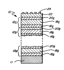
FIGURE 1 is a fragmentary, cross-sectional
view of a tandem photovoltaic device, said device
comprising a plurality of p-i-n type cells, each layer
of the cells formed from a semiconductor alloy
materjal;
FIGURE 2A is a schematic representation of a
constant approximately l.SeV optical bandgap solar
cell (sample No. 2130) with associated interfacial and
buffer layers, which cell is intended to serve as the
reference point for measuring the improved solar cell
design of the instant invention;
FIGURE 2B is an IV curve of the constant
approximately l.SeV optical bandgap solar cell of
Figure 2A measured under 700 nanometer illumination,
said curve illustrating the measured VOc. Jsc and
fill factor of said cell;
FIGURE 3A is a schematic representation of an
about 3000 angstrom thick, graded, approximately
1.5-1.7eV optical bandgap solar cell (sample No. 2169)
with associated interfacial and buffer layers;
FIGURE 3B is an IV curve of the about 3000
angstrom thick, graded, approximately 1.5-1.7eV
optical bandgap solar cell of Figure 3A measured under
700 nanometer illumination, said curve illustrating
the measured VOc. Jsc~ and fill factor of said
cell;
FIGURE 4A is a schematic representation of an
about 4000 angstrom thick, graded, approximately
1.5-1.7eV optical bandgap solar cell (sample No. 2171)
with associated interfacial and buffer layers
.
:
:
,:
.
-~ :
S0-241
~289232
-18-
FIGURE 4B is an IV curve of the about 4000
angstrom thick, graded, approximately 1.5-1.7eV
optical bandgap solar cell of Figure 4A measured under
700 nanometer illumination, said curve illustrating
the measured VOC~ Jsc and fill factor of said
cell;
FIGURE SA is a schematic representation of an
about 5000 angstrom thick, graded, approximately
1.5-1.7eV optical bandgap solar cell (sample No. 2172)
10 with associated interfacial and buffer layers,
FIGURE 5B is an IV curve of the about 5000
angstrom thick, graded, approximately 1.5-1.7eV
optical bandgap solar cell of Figure 5A measured under
700 nanometer illumination, said curve illustrating
the measured VOC~ Jsc and fill factor of said
cell;
FIGURE 6A is a schematic representation of an
about 3000 angstrom thick, graded (with the wider
bandgap at the p+ layer), approximately 1.5-1.7eV
20 optical bandgap solar cell (sample No. 2174) with
associated interfacial and buffer layers;
FIGURE 6B is an IV curve of the about 3000
angstrom thick, graded (with the wider bandgap at the
p+ layer), approximately 1.5-1.7eV optical bandgap
solar cell of Figure 6A measured under AMl.5
illumination, said curve illustrating the measured
Voc Jsc and fill factor of said cell; and
FIGURE 7A is a schematic representation of an
about 5500 angstrom thick, spatially modulated,
30 approximately 1.5-1.7eV optical bandgap solar cell
(sample No. 2191) with associated interfacial and
buffer layers;
:
S0-241 1289232
-1 9-
FIGURE 7B is an IV curve of the about 5500
angstrom thick, spatially modulated, approximately
1.5-1.7eV optical bandgap solar cell of Figure 7A
measured under AMl.5 illumination, said curve
illustrating the measured VOc. Jsc and fill factor
of said cell;
FIGURE 8A is a schematic representation of an
about 5500 angstrom thick, spatially modulated,
approximately 1.5-1.7eV optical bandgap solar cell
(sample No. 2190) with associated interfacial and
buffer layers;
FIGURE 8B is an IV curve of the about 5500
angstrom thick, spatially modulated, approximately
1.5-1.7eV optical bandgap solar cell of Figure 8A
measured under AMl.5 illumination, said curve
illustrating the measured VOC, Jsc and fill
factor of said cell;
FIGURE 9A is a schematic representation of an
about 5000 angstrom thick, spatially modulated,
approximately 1.5-1.7eV optical bandgap solar cell
(sample No. 2195) with associated interfacial and
buffer layers which cell is intended to serve as the
reference point for measuring the improved solar cell
design of the instant invention;
FIGURE 9B is an IV curve of the about 5000
angstrom thick, spatially modulated, approximately
1.5-1.7eV optical bandgap solar cell of Figure 9A,
said curve illustrating the measured VOC~ Jsc and
fill factor of said cell.
.
.
.'
S0-241
1289232
-20-
DETAILED DESCRIPTION OF THE DRAWINGS
1. The Photovoltaic Cell
Referring now to the drawings and
particularly to Figure 1, a photovoltaic cell, formed
of a plurality of successively deposited p-i-n layers,
each of which includes, preferably, a thin film layer
of semiconductor alloy material, and at least one of
said layers formed of n-doped and p-doped wide
bandgap, microcrystalline semiconductor alloy material
is shown generally by the reference numeral 10.
More particularly, Figure 1 shows a p-i-n
type photovoltaic device such as a solar cell made up
of individual p-i-n type cells 12a, 12b and 12c.
Below the lowermost cell 12a is a substrate 11 which
may be transparent or formed from a metallic material
such as stainless steel, aluminum, tantalum ,
molybdenum, chrome or metallic particles imbedded
within an insulator. Although certain applications
may require a thin oxide layer and/or a series of base
contacts prior to the application of the amorphous
material, for purposes of this application, the term
"substrate" shall include not only a flexible film,
but also any elements added thereto by preliminary
processing. Also included within the scope of the
present invention are substrates formed of glass or a
glass-like material, such as a synthetic polymeric
resin on which an electrically conductive electrode is
applied.
Each of the cells 12a, 12b and 12c are
preferably fabricated within film semiconductor bodies
containing at least a silicon alloy material. Each of
the semiconductor bodies includes an n-type
conductivity semiconductor layer 20a, 20b and 20c; a
substantially intrinsic semiconductor layer 18a, 18b
.
.
: ` ' '
,~
S0-241
1289232
- 2 l -
and 18c; and a p-type conductivity semiconductor layer
16a, 16b and 16c. Note that the intrinsic layer may
include traces of n-type or p-type dopant material
without forfeiting its characteristic neutrality;
hence it may be referred to herein as a "substantially
intrinsic layer". As illustrated, cell 12b is an
intermediate cell and as indicated in Figure 1,
additional intermediate cells may be stacked atop the
illustrated cells without departing from the spirit or
scope of the present invention. Also, although p-i-n
photovoltaic cells are illustrated, the methods and
materials disclosed herein may also be utilized to
produce single or multiple n-i-n cells and p-n cells.
It is to be understood that following the
deposition of the semiconductor alloy layers a further
deposition process may be either performed in a
separate environment or as part of the continuous
process. In this step, a TC0 (transparent conductive
oxide) layer is added. An electrode grid may be added
to the device where the cells of a sufficiently large
area or if the conductivity of a TC0 layer is
insufficient. The grid 24 is adapted to shorten the
carrier path and increase the conduction efficiency of
photogenerated charge carriers.
EXAMPLES
Specific examples will now be presented to
illustrate the potential ramifications which the
concepts of the instant invention may have on the
broad field of amorphous silicon alloy solar cell
design. While specific reference will be made to
single p-i-n type thin film photovoltaic cells, it is
to be understood that the aforementioned ramifications
of the inventive concepts disclosed herein have the
~ most significance when applied to double and triple
-~ ~ stacked photovoltaic structures (of particular
'~
, ~: .: '
:: .
S0-241 128~23Z
-22-
importance is an improved 1.5eV bottommost solar cell
of a dual bandgap triple stacked photovoltaic
structure and an improved 1.5eV or lower bandgap solar
cell for the middle and bottommost cells of a triple
bandgap, triple stacked photovoltaic structure).
Regardless of final structural configuration,
the p-type, intrinsic and n-type layers of such single
cells will be fabricated from a similar variety of
precursor process gases, (such as silane, disilane,
silicon tetrafluoride, germane, phosphine, boron
trifluoride, argon and hydrogen), which gaseous
precursor combinations are deposited onto a small area
plate of substrate material. As used, in each of the
following examples, the plate of substrate material is
highly polished number 430 stainless steel. In order
to provide for the back reflection of nonabsorbed
photons of the incident solar spectrum, there is
deposited (as by sputtering atop said plate of
stainless steel) a thin layer of highly reflective,
specular silver to a uniform thickness of
approximately 1000 angstroms (thick enough to obtain
coverage despite the agglomerative nature of the
silver material). In most cases, the sputtering
process is carried out at a nominal substrate
temperature of about 200 degrees Centigrade, at which
temperature a slightly textured deposition surface is
created (hereinafter referred to as "an ordinary back
reflector"). However, in those instances in which
optimum solar cell performance is to be measured, the
substrate temperature is raised to about 600 degrees
Centigrade to provide a back reflective layer
characterized by optimum feature si~es to promote
photon scattering at angles adapted to deliver total
internal reflection of incident photons.
so - 24 1 1.289232
-23-
Deposited atop said 1000 angstrom thick layer
of textured silver, is a layer of zinc oxide. The
layer of zinc oxide is sputter deposited, in a
conventional fashion, to a uniform thickness of
approximately 5000 angstroms at temperatures of about
400 degrees Centigrade. This 5000 angstrom thick
layer is transparent, conductive, prevents
interdiffusion of the subjacent layer of silver and
the superjacent layer of amorphous silicon alloy
material and interacts with the textured silver to
enhance the light capturing properties so as to
achieve the aforementioned goal of total internal
reflection.
The detailed processes by which the n-i-p
type photovoltaic structure of the instant invention
can be fabricated and the observed values of critical
cell operational characteristics (such as open circuit
voltage, short circuit current and fill factor) are
set forth in the detailed examples which follow
hereinbelow. It is to be specifically noted that, and
as should be evident from the foregoing sections of
the specification, it is the design of the intrinsic
layer and associated interfacial buffer layers which
will be modified so as to enhance open circuit
voltage, short circuit current and/or fill factor
toward the ultimate goal of improved multigap,
spectrum splitting solar cell efficiency.
EXAMPLE I
The p-i-n type photovoltaic cell of this
example is formed with a constant optical bandgap
intrinsic layer of about 1.5eV, amorphous silicon
germanium alloy material. It is intended that said
cell will serve as the base line or standard reference
point by which the more innovative designs of the
subject invention may be measured. It is to be kept
~ ::
. .
' '
,~ ,
:
- ~ .
289232
-24-
in mind that the specific values of cell performance
derived from the cell fabrication process detailed in
this Exa~ple I are typical of those expected from
state-of-the art cells fabricated with about 1.5eV
intrinsic layers. Said cell was identified in the
inventor~s laboratory notebook as sample Number 2130.
This n-i-p type cell was prepared in the
following manner. The small area plate of substrate
material with the dual layered back reflective
materials deposited thereupon was placed in an
evacuated deposition chamber, which chamber was held
at approximately 300 degrees Centigrade and at a
pressure of about 0.6 Torr. Thereafter, the following
precursor process gases were introduced into said
chamber at the following flow rates so as to effect
the deposition of the n-type layer of silicon hydrogen
alloy material:
Gas flow Rate
~ane (SiH ) 0.2 SCCM
Phosphine (~H3) 0.4 SCCM
(lX phosphine diluted
in H~)
Argon ~Ar) 39.4 SCCM
The plate of substrate material and precursor
process gases were then energized by a 1.5 watt source
of 13.56 MHz RF energy for approximately three (3)
minutes. The result of this process was the
deposition of said 150-200 angstrom thick layer of
n-type amorphous silicon hydrogen alloy material.
~ hile the n+ layers in these patent examples
have been fabricated solely utilizing amorphous
layers, we anticipate that with a microcrystalline n+
: layer, as desc~ibed in applicant's copending Canadian Patent
Application Serial No. 566,0S~ filed May 5, 1988 for "N-type
Microcrystalline Semiconductor Alloy Including Bank Gap Widening
Elements, Methods of Fabricating Same, And Devices Utilizing Same"
, ~ .
cell
.
~'
.
:
, . .
,
1289232
parameters, for example VOc and fill factor will be
improved. This improvement is due to the high built
in field and the wide optical bandgap.
Prior to the deposition of said intrinsic
layer of amorphous silicon germanium alloy material,
it is necessary to specially treat the exposed surface
of the n+ layer so as to reduce interfacial
recombination. In connection therewith, it is to be
understood that both the n-layer/intrinsic layer
interface, as well as the p layer/intrinsic layer
interface are formed with specific interfacial buffer
layers, said buffer layers being fabricated from
substantially intrinsic layer precursor process gases
(for depositing low defect density material), which
gases are introduced into the deposition chamber in
the following ratios and at the following flow rates:
Gas Flow Rat-e
Disilane (Si2H6) 0.55 SCCM
Boron tri-fluoride (BF3) 0.3 SCCM
in H2)
Hydrogen (H2) 48.0 SCCM
Germane (GeH4) Ramped from 0.0
SCCM to 0.3 SCCM
over 1 minute,
held at 0.3 SCCM
for 27.5 minutes,
; and ramped from
0~3 SCCM to 0.0
SCCM over 1.5
minutes
It is important to note that the germane
(GeH4) inlet valve remains open during the entire 30
minute interval, although the flow rate is increased
and decreased via a manual flow control. This
procedure has the effect of preventing a germane
pressure "spike" when the gas is first introduced into
the deposition chamber and has the further effect of
So-241 1289232
providing for the smooth introduction of vanishingly
small amounts of germanium into the top and bottom
buffer layers. Note that the purpose of the
interfacial buffer layers is to reduce the interfacial
recombination of photogenerated charge carriers by
eliminating the presence of a sharp transitian zone or
spike which would otherwise exist between the wide
bandgap doped layers of microcrystalline silicon alloy
material and the more narrow optical bandgap layer of
intrinsic amorphous silicon alloy material.
In order to effectuate the deposition of the
intrinsic layer, the plate of substrate material with
the dual-layered back reflector and the n-type layer
deposited thereupon is subjected to deposition
conditions substantially similar to those described
above (about 300 C, about 1.2 Torr and about 1
watt) in the presence of a mixture of precursor
process gases adapted to glow discharge deposit an
intrinsic layer of amorphous silicon germanium
hydrogen fluorine material. The bottom, interfacial
buffer layer is formed during the first minute of the
intrinsic layer deposition process by progressively
increasing the germane (GeH4) gas flow rate from
about 0.0 SCCM to about 0.3 SCCM while maintaining the
flow rates of the other feedstock gases constant. The
resulting interfacial layer of steadily increasing
germanium content is again intended to provide a
smooth transition between the 1.5eV optical bandgap
intrinsic layer and the wider bandgap buffer layer so
as to avoid the presence of an impediment to charge
carrier movement. Said interfacial layer is
essentially an amorphous silicon hydrogen alloy
material with trace amounts of boron and fluorine and
gradually increasing germanium content, which layer is
~ deposited for a period of about 60 seconds so as to
: .
.
: ~
~ - . :
~ ~ .
.
So-241 i.289232
-27-
assume a total thickness of approximately 100
angstroms.
The 1.5eV bandgap intrinsic layer is formed
during the 27.5 minutes period immediately following
the deposition of the bottom interfacial layer.
During this period all of the aforementioned
deposition conditions, as defined above, are held
constant, including the flow rate of the germane (at
about 0.3 SCCM). The result is the deposition of a
layer of a substantially intrinsic, amorphous silicon
germanium hydrogen fluorine alloy material, said
intrinsic layer deposited to a thickness of
approximately 2750 angstroms. It is noteworthy that
this is the active photogenerative layer of the solar
cell and is therefore the layer of the cell in which
the density of defect states should be reduced to a
minimum; however, due to the fact that the germanium
content is about 30X to 40% so as to provide about
l.5eV bandgap amorphous silicon germanium alloy
material, the density of states is higher than that of
non-germanium containing intrinsic silicon alloy
material. The reasons that the defect density
increases with increasing germanium content has been
explained hereinabove, and need not be detailed
again. However, this increased defect density must be
taken into consideration in the intrinsic layer
designs disclosed in the Examples which follow.
Immediately following the 27.5 minute
intrinsic layer deposition period, the germane flow
rate is ramped down from about 0.3 SCCM to about 0.0
SCCM over approximately a 1.5 minute time period,
which slow ramp down period results in the formation
of a top interfacial layer in contact with the
subsequently deposited p~ layer. This interfacial
layer is formed of an amorphous silicon fluorine
,:
~, ~
, .
: `:
.
. :. . .
,
:
. .
: ~'
.
S0-241
~289Z32
-28-
hydrogen boron alloy material (without germanium) so
as to eliminate a spiked condition in the bandgap
thereof which would impede charge carrier collection.
Thereafter, the flow rate of all of the remaining
intrinsic layer process gases are reduced to about 0.0
SCCM, and a hydrogen plasma is ;nitiated. Said
hydrogen plasma is maintained for approximately 30
seconds, during which time period the activated
hydrogen diffuses through the uppermost portion of the
previously deposited intrinsic layer for the purpose
of satisfying dangling bonds and other defect states
and further reducing intrafacial recombination of
charge carriers moving past the intrinsic layer/p~
layer interface. This hydrogen plasma further creates
a clean surface upon which nucleating centers for the
subsequent growth of p-type microcrystalline
material. A clean surface is believed to be necessary
due to the fact the growth of crystallites must occur
in a layer which is only on the order of 100 angstroms
thick.
The last layer of the thin film solar cell to
be deposited is the light incident p-type layer, which
layer is disposed atop the hydrogen plasma layer.
Said p+-layer is deposited at 25 watts of 13.56 MHz RF
energy at a nominal substrate temperature of about 250
; degrees Centigrade and a pressure of about 2 Torr.
The p+-layer precursor process gases are then
introduced into the deposition chamber in the
following ratios and the following flow rates.
Gas Flow Rate
Boron tri-fluoride1.0 SCCM
40 ppm BF3, diluted
in H2
Silane (SiH4) 1.0 SCCM
Hydrogen (H2) 48.0 SCCM
;
:
S0-241 1289232
-29-
Said precursor or feedstock gases are exposed
to said 25 watt source of RF power for approximately
50 seconds, thereby resulting in the deposition of
about a 100 angstrom thick layer of heavily p-doped
microcrystalline silicon hydrogen fluorine material.
Due to the high volume fraction of crystallites, this
p+ layer exhibits a high conductivity of about 1-10
ohms lcm 1 and a wide optical bandgap of about
2.0eV so as to provide, in conjunction with the
microcrystalline n+ layer, a strong built-in potential
across the photogenerative intrinsic layer of the
solar cell, which built-in potential aids in charge
carrier collection and in splitting the quasi-Fermi
level of said intrinsic layer.
The type of deposition process described
hereinabove, results in the fabrication of about a
1.5eV optical bandgap, O.OS square centimeter (these
small area devices are fabricated and tested without
the presence of silver conducting grid linesj, n-i-p
photovoltaic device; which device was characterized by
the following tabularized electrical data:
TABLE
(Sample 2130, Example I)
Illumination AMl.5 700 nm Red=Blue
Jsc 2 19.520 9.366 1.661, 1.657
(mA/cm )
VOC 0.783 0.747 0.674, 0.688
(Volts)
Fill Factor 0.518 0.506 0.574, 0.658
Note that 700 nanometer (deep red) light was
used because a 1.5eV bandgap solar cell, when employed
in a t-andem photovoltaic device structure, will see
this wavelength of light; the shorter, more energetic
blue wavelengths being absorbed in the uppermost
cell(s) of the device. A schematic illustration of
~: :
.. . . . . . .
- .. ~ ~ :
- - . .
. - - ;
50-241 1289232
-30-
the aforedescribed solar cell design is provided in
Figure 2A, with the IV curve thereof, as measured
under 700 nanometer light, provided in Figure 2B.
Note that this cell was also measured under (and the
results tabulated hereinabove) AMl.5 illumination,
which illumination is not red wavelength limited.
Finally, note that this cell was also measured (and
the results tabulated hereinabove) by substantially
equalizing the photogenerated current due to blue
photons and the photogenerated current to red photons
of incident radiation. This equalization of blue and
red current provides very useful information
concerning the collection of photogenera~ed blue and
red photons. For instance, a low blue fill factor is
indicative of back diffusion of electrons into the p+
layer, while a low red fill factor is indicative of
poor hole transport.
Again, the solar cell operational values set
forth hereinabove provide the reference point or
baseline against which the solar cell designs set
forth in the following Examples will be evaluated.
EXAMPLE II
A second n-i-p type solar cell sample,
identified in the inventors lab book as sample number
2169, was prepared using essentially the same recipes
; as described hereinabove with respect to Example I.
There were, however, significant changes in the
design of the intrinsic layer of said cell, which
changes necessitated the graded introduction and of
feedstock gases. Of course, it is to be understood
that due to the graded design of the intrinsic layer,
further modifications of buffer layers, interfacial
layers, boron content in the intrinsic layer, etc.
will be necessary in order to optimize the instant
invention. In the instant example, the n-layer of
S0-241
-31-
amorphous silicon alloy material was deposited for
only a two minute period so as to limit the thickness
thereof to approximately ~00 to 150 angstroms.
As mentioned in the previous paragraph, the
major change in the cell configuration occurred in the
design of the narrow bandgap layer of intrinsic
amorphous silicon germanium alloy material.
Particularly, the precursor process gas mixture was
free of boron tri-fluoride; and the ramp-in time of
the germane gas so as to reach the appropriate
concentration for the fabrication of 1.5eV bandgap
material was increased from 1 minute to 29 minutes.
Thus the gases introduced into the deposition chamber
and the respective flow rates thereof were as follows:
Gas Flow Rate
Disilane (Si2H6) 0.5 SCCM
Hydrogen (H2) 48.0 SCCM
Germane (GeH4) Ramped from 0.0
SCCM to 0.3 SCCM
over 29 minutes,
then ramped down
from 0.3 SCCM to
0.0 SCCM over 1
minute.
It therefore becomes apparent that the graded
introduction of the germane was effected over a
significantly longer period of time, vis-a-vis, the
introduction of germane in the constant bandgap sample
of Example I. It is to be further noted that the step
of depositing a bottom buffer layer has been
eliminated. The results which will be set forth
hereinafter are to be analyzed in view of the fact
.
, ,
,
, .,
: . .
' ~ ,
. .
~, ' : . . . . - - :
::: .: . : ,
;: ~ :. .
,
S0-241 1Z8923Z
-32-
that no source of boron, such as BF3, was introduced
into the intrinsic layer to aid in the collection of
holes photogenerated therein. Through the process
outlined in this example, the instant inventors have
profiled the the bandgap of the intrinsic layer of the
photovoltaic device, grading said device (over a
thickness of about 3000 angstroms) from a maximum of
about 1.7eV adjacent the n-layer interface to a
minimum of about to 1.5eV adjacent the p-layer
10 interface. A schematic diagram of this cell design is
illustrated in Figure 3A with the IV curve thereof
measured under 700 nanometer light provided in Figure
3B.
The changes in the design of the intrinsic
layer, described hereinabove, resulted in significant
improvements in the performance of the n-i-p
photovoltaic device, which improvements are tabulated
hereinbelow:
TABLE
(Sample 2169, Example II)
Illumination AMl.5 700 nm Red=Blue
Jsc 2 17.057 8.968 1.511, 1.516
(mA/cm
Voc 0.799 0.779 0.699, 0.703
(Volts)
Fill Factor0.590 0.590 0.661, 0.674
While the short circuit current was slightly
lower than in the base line case cell of Example I,
30 hereinabove, it is remarkable that even though no
boron has been added in the intrinsic layer, the fill
factor has been significantly improved. This can only
be attributed to the field gradient which aids in hole
transport and hence charge carrier collection. It is
also important to note that the fill factor can be
S0-241 12~2~
-33-
further improved through the addition a slight boron
gradient through the intrinsic layer. This is
particularly important in view of the fact that the
short circuit current of a cell can be improved by
increasing the thickness of the intrinsic layer
thereof; however, said increased thickness makes it
all the ~ore necessary to add boron. This is because,
under red illuminat~on, charge carriers are
photogenerated throughout the bulk of the intrinsic
layer and holes have to make a successful journey all
the way to the p+ layer in order to be collected.
Therefore the addition of boron will not only improve
the fill factor, but will improve hole transport to
also provide for the fabrication of a thicker
intrinsic layer so as to enhance Jsc
EXAMPLE III
The present inventors prepared a third sample
identified in their lab notebook as sample number
2171. The method employed in preparing said sample is
substantially identical to that described hereinabove
in describing the fabrication of sample No. 2169 of
Example II. The only change in deposition parameters
in the preparation of instant sample number 2171 was
to increase the time period in which the germane flow
rate was ramped from 0.0 SCCM to 0.3 SCCM so that
additional photons of deep red light could be
collected so as to enhance short circuit current
density, Jsc More particularly, said ramping
function was accomplished over a 39 minute time
period, instead of the 29 minute time period set forth
in Example II. All other deposition parameters
remained constant. In this manner, a substantially
4000~angstrom thick intrinsic layer of silicon
germanium alloy material was deposited, which
intrinsic layer was profiled from a maximum bandgap
~ .
~ :
: ~
. -
.
S0-241 12892~2
-34-
portion of about 1.7eV adjacent the n-layer interface
to a minimum bandgap portion of about 1.5eV adjacent
the p-layer interface. A schematic diagram of this
cell design, including the profiled intrinsic layer,
is illustrated in Figure 4A, with the IV curve thereof
as measured under 700 nanometer illumination provided
in Figure 4B.
The fabrication process employed in the
manufacture of sample number 2171 resulted in the
design of an n-i-p photovoltaic device with
improvements in electrical parameters which are
tabulated hereinbelow:
TABLE
(Sample 2171, Example III)
Illumination AMl.5 700 nm Red=Blue
Jsc 18.212 9.396 1.498, 1.408
(mA/cm2)
Voc 0.790 0.761 0.685, 0.688
(Volts)
fill Factor 0.537 0.573 0.645, 0.621
These results demonstrate significant
improvement over the standard amorphous
silicon:germanium all~oy photovoltaic cell of Example
I. It is interesting to note that even though the
sample cell is thicker than the cell described in
Example I, the fill factor is still higher because of
the graded field which aids in charge carrier
movement. Further, and, as predicted, the thicker
intrinsic layer of the instant sample resulted in an
; 30 increase in photogenerated short circuit current
~ vis-a-vis the Example II cell.
~ ,::
:~; :
:.;
:,:~ ~ : . ,- .
,
,
. - :
- - . .~, . . : ~ ,
, - ` . :
.
S0-241 1289232
-35-
EXAMPLE IV
The present inventors further prepared a
fourth sample identified in their lab notebook as
sample number 2172. Sample No. 2172 was prepared in
essentially the same manner as described hereinabove
with reference to sample number 2171. The only change
in deposition parameters in the preparation of the
instant sample was to increase the time period in
which the germane flow rate was ramped from about 0.0
10 SCCM to about 0.3 SCCM. More particularly, the
ramping function was accomplished over a 49 minute
time period prior to being ramped down from about 0.3
SCCM to about 0.0 SCCM over a 1 minute time period.
In this manner, and with all other parameters
unchanged, a substantially 5000 angstrom thick
intrinsic layer of silicon germanium alloy material
was deposited, with said intrinsic layer being
profiled from a maximum optical bandgap of about 1.7eV
adjacent the n-layer interface to a minimum bandgap of
20 about 1.5eY adjacent the p-layer interface. A
schematic diagram of this cell design including the
profiled intrinsic layer, is illustrated in Figure 5A
with the IV curve thereof measured under 700 nanometer
illumination provided in Figure 5B.
The fabrication process employed in the
manufacture of sample No. 2172 resulted in the design
of a n-i-p photovoltaic device which demonstrated the
following electrical characteristics tabulated
hereinbelow:
.
S0-241 1289232
-36-
TABLE
(Sample 2172, Example IV)
Illumination AMl.5 700 nm Red=Blue
Jsc 2 19.053 9.869 1.527, 1.512
(mA/cm )
Voc 0.793 0.762 0.686, 0.696
(Volts)
Fill Factor 0.544 0.540 0.624, 0.657
As can be observed by comparing the
performance values for sample 2172 disclosed in the
instant Example with those performance values
disclosed for the base line cell, sample 2130 of
Example I, both the fill factor and the VOC are
above the values measured for said standard amorphous
silicon:germanium alloy intrinsic layer cell of
Example I. As predicted, the value of the short
circuit current continues to increase with the
thickness of the graded intrinsic layers and this
increase is not offset by a reduced fill factor which
is also greater than that of Example I. Moreover, the
open circuit voltage has not decreased relative to
that measured in Example III. Note that as the
thickness of the cell increases, some loss in VOC
can be predicted due to the recombination caused by
that additional thickness; therefore, it is not
surprising that the 3000 angstrom thick intrinsic
layer cell of Example II would develop a higher VOC
then that of Examples III and IV.
EXAMPLE V
A fifth sample, designated by the lab
notebook sample number 2174 was fabricated in
substantial accordance with the deposition process
outlined in Example II, described hereinabove with
respect to sample No. 2169. However, the instant
sample No. 2174 was prepared in such a manner that the
.
.
.'
'
S0-241 12892~2
intrinsic layer of silicon germanium alloy material
there was gradingly fabricated with the about 1.7eV
wider bandgap material disposed adjacent the p+ layer
of microcrystalline material and the about 1.5eV
narrower bandgap material disposed adjacent the n+
layer of amorphous material. More particularly,
following the deposition of the n+ layer, the germane
gas was ramped from about 0.3 SCCM adjacent said n+
layer interface to about 0.00 SCCM adjacent the p+
layer over a time period of approximately 29 minutes.
The top buffer layer was then deposited by continuing
the glow discharge (without introducing any germane
gas flow) so as to provide an interfacial buffer
between the p+ layer and the intrinsic layer, which
buffer layer, as detailed previously, is adapted to
reduce the recombination of photogenerated charge
carriers at said intrinsic/p+ layer interface. A
schematic diagram of this cell design, including the
bandgap profiled intrinsic layer of the instant
invention, having an overall intrinsic layer thickness
of about 3000 angstroms~ is illustrated in Figure 6A,
with the TV curve thereof, as measured under AMl.5
illumination, provided in Figure 6B.
The n-i-p photovoltaic device fabricated in
this manner, with the bandgap thereof graded from a
maximum at the p+ layer interface, demonstrated solar
cell performance characteristics showing remarkable
open circuit voltage. Specifically, this solar cell
provided the following measured electrical
characteristics tabulated hereinbelow:
.
S0-241
1289Z32
- 3 8 -
TABLE
(Sample 2174, Example V)
Illumination AMl.5 700 nm Red=Blue
~sc 2 16.444 7.670 1.570, 1.628
(mA/cm )
Voc 0.860 0.805 0.738, 0.778
(Volts)
Fill Factor 0.465 0.418 0.462, 0.678
The truly intriguing result was the very high
open circuit voltage value of 0.860 volts, which value
must be compared with the value of 0.747 volts set
forth in Example I for the base-line solar cell, an
increase of 113 millivolts. The fill factor is lower
than in the standard cell of Example I, but it can be
improved by optimizing the boron profiling in the
intrinsic layer.
EXAMPLE VI
As can be seen from a review of the foregoing
examples, in the first case the instant inventors have
provided a substantial increase in VOC by
operatively disposing the wide~bandgap portian of the
intrinsic layer adjacent the light incident doped
layer of the cell (although the fill factor
decreased); in the second case, the instant inventors
have provided a substantial improvement in Jsc and
f111 factor (although the improvement in ~oc was
only marginally enhanced). Therefore, in this
Example, the intrinsic layer was spatially modulated
from a widest bandgap at the light incident doped
~ 30 layer, quickly ramped down to a minimum bandgap
-~ ~ portion, then slowly ramped back up to a widest
; bandgap at the~opposite doped layer. In this manner,
the inventors were seeking to ~marryU the performance
of the two cases set forth hereinabove so as to
significantly improve every critical electrical
characteristic of solar cell performance.
,, ~: , :
. .
~: . .. .
. .
. - :
:: ' : ' . -
S0-241 I 2 8 g 2 3 2
-39-
A sixth sample, designated by the lab
notebook number 2191, was fabricated according to the
process described hereinabove for Examples II-V. In
this Exa~ple, the time of deposition and the germane
flow rate for the intrinsic layer was varied relative
to the process described in Example IV. More
particularly, following the deposition of the n+ layer
of microcrystalline silicon alloy material, the
intrinsic layer of germanium silicon alloy material is
formed in a 55 minute deposition process wherein the
germane flow rate is ramped from about 0.0 SCCM at the
n+ layer interface up to about 0.3 SCCM over a fifty
minute time interval, and is then ramped from about
0.3 SCCM to about 0.0 SCCM at the p+ layer interface
over a 5 minute time interval. The resulting
intrinsic layer is characterized by a bandgap which is
graded from about 1.7eV adjacent the n+ layer, down to
about 1.5eV centrally thereof and then back up to
about about 1.7eV adjacent the p-layer interface.
After the ramping down to about a 0.00 SCCM flow of
germane has been completed, a top buffer layer is
deposited by introducing the intrinsic layer feedstock
gases (absent said germanium-containing precursor). A
schematic diagram of this spatially modulated cell
design, including the double profiled intrinsic layer
having an overall thickness of about 5500 angstroms,
is illustrated in Figure 7A with the IV curve thereof,
as measured under AMl.5 illumination, provided in
Figure 7B.
The n-i-p photovoltaic device fabricated in
this manner demonstrated characteristics superior to
those of all of the graded or constant bandgap
photovoltaic devices described hereinabove.
Specifically, said double profiled (DPI, Double
Profiled Instrinsic layer) cell was fabricated with
the following measured electrical characteristics
tabulated hereinbelow:
`
... .
S0-241
1289232
-40-
TABLE
(Sample 2191, Example VI)
Illumination AMl.5 700 nm Red=Blue
Jsc 2 20.432 10.468 1.797, 1.765
(mA/cm )
Voc 0.838 0.802 0.737, 0.756
(Volts)
Fill Factor 0.511 0.475 0.552, 0.710
This provided a solar cell photoconversion
efficiency of 9.6879. If this efficiency is
normalized to demonstrate performance under AMl
illumination (a gain of 7X in intensity of incident
radiation), the cell would measure an efficiency of
about 10.37%, a NEW WORLD RECORD for a l.5eV bandgap
amorphous silicon germanium alloy solar cell.
Finally, note that when the blue and red currents
photogenerated under 700 nanometer illumination are
matched, (1) a large enhancement in VOc can be seen;
however (2) the red fill factor is only about 0.546,
thereby indicating problems in hole transport to the
p+ layer. Again, a solution to the problem of hole
collection would be the boron doping of the intrinsic
layer which could be utilized to improve hole
transport.
It must be explained that the plate of
substrate material utilized for this experiment had
deposited thereupon the best possible back reflector,
i.e., a textured back reflector characterized by
substantially ideal surface features to provide for
scattering of photons at optimum angles from the
textured surface thereof.
S0-241
128g232
-41-
EXAMPLE VII
A seventh sample, designated by the lab
notebook sample number 2190 was fabricated in
substantial accordance with the deposition process
outlined in detail with respect to sample No. 2191
hereinabove. This Example varies from Example VI only
in the length of time in which the intrinsic layer of
silicon germanium alloy material was ramped from the
minimum optical bandgap value of about 1.5eV to a
bandgap value of about 1.7eV adjacent the p+ layer
interface. More particularly, following the
deposition of the n+ layer of amorphous silicon alloy
material, the intrinsic layer is formed in a 55 minute
deposition process wherein the germane flow rate is
ramped from about 0.0 SCCM adjacent the n+ layer
interface up to about 0.3 SCCM over about a 50 minute
time interval and then is ramped down from about 0.3
SCCM to about 0.00 SCCM adjacent the p+ layer
interface over about a 2 minute time interval. The
one minute non-germanium containing plasma then
completes the deposition of the intrinsic layer. A
schematic diagram of this spatially modulated cell
design, including the double profiled intrinsic layer,
having an overall thickness of about 5200 angstroms,
is illustrated in Figure 8A with the IV curve thereof,
as measured under AMl.5 illumination, provided in
Figure 88.
The n-i-p photovoltaic device fabricated in
this manner demonstrated solar cell performance
characteristics marginally superior to those set forth
in the world record cell detailed in Example V
hereinabove. Specifically, said double profiled
intrinsic (DPI) cell provided the following measured
electrical characteristics tabulated hereinbeiow:
SO-241
12892~2
-42-
TABLE
(Sample 2190, Example VII)
Illumination AMl.5 700 nm Red=Blue
Jsc 2 20.120 10.453 1.698, 1.696
(mA/cm )
Voc 0.804 0.770 0.687, 0.702
(Volts)
Fill Factor 0.515 0.527 0.601, 0.652
The AMl.5 measurements calculate to a photoconversion
10 efficiency of about 9.760%. Again, by converting this
photoconversion efficiency measured under AMl.5
illumination to AMl illumination, the efficiency
measures about 10.44%, another WORLD RECORD for an
approximately 1.5eV bandgap solar cell. Once again,
room for further improvement is apparent because no
boron has been added to the intrinsic layer in order
to improve hole conduction.
EXAMPLE VIII
An eighth sample, designated by the lab
20 notebook sample number 2195 was fabricated in
substantial accordance with the deposition process
outlined in detail with respect to sample 2191
(Example VI) hereinabove. This Example differs from
Example VI only in the addition of a boron-containing
precursor to the gaseous mixture for depositing the
intrinsic layer of silicon germanium alloy material.
Further, the boron precursor was graded so as to
correspond to the profile of the germanium in the
intrinsic layer. More particularly, following the
30 deposition of the n+ layer of amorphous silicon alloy
material, the intrinsic layer is formed in a 55 minute
deposition process wherein the germane flow rate is
ramped up from about 0.0 SCCM adjacent the n+ layer
interface up to about 0.3 SCCM over about a 50 minute
time interval and then is ramped down from about 0.3
SO-241 1289232
-43-
SCCM to about 0.00 SCCM adjacent the p~ layer
interface over about a 2 minute time interval. During
the deposition of the intrinsic layer, about 0.2 SCCM
of BF3 is added to the gaseous precursor mixture for
30 minutes and then the flow rate of BF3 is ramped
up to about 0.4 SCCM. The one minute non-germanium
containing plasma then completes the deposition of the
intrinsic layer. A schematic diagram of this
spatially modulated cell design, including the double
profiled intrinsic layer, having an overall thickness
of about 5200 angstroms, is illustrated in Figure 9A
with the IV curve thereof, as measured under AMl.5
illumination, provided in Figure 9B.
The n-i-p photovoltaic device fabricated in
this manner demonstrated solar cell performance
characteristics under red illumination superior to
those set forth in the world record cell detailed in
Example VI and YI I ereinabove. Specifically, said
double profiled intrinsic (DPI) layer with profiled
dopant provided the following electrical
characteristics tabulated hereinbelow:
TABLE
(Sample 2195, Example VIII )
Illumination AMl.5 700 nm Red=Blue
Jsc 2 19.880 10.582 2.124, 2.106
(mA/cm )
Y 0.831 0.798 0.740, 0.756
oc
(Volts)
Fill Factor 0.533 0.499 0.585, 0.697
The AMl.5 measurements calculate to a solar cell
photoconversion efficiency of about 8.806. Again, by
converting this efficiency to AMl illuminatiqn, the
~- efficiency measures about 10.3% another WORLD RECORD
for an approximately 1.5èY bandgap solar cell. Note
that, as predicted hereinabove, the addition of a
~,; ~.... . ... .
.
, ~ . . . ' ' ': " : ,',
.~, , ' ' ' ~ - , '
-
S0-241
1289232
-44-
boron gradient provided a "boost" to hole movement in
the region of the intrinsic layer which has the
greatest defect density (the narrowmost bandgap
material) and thereby improved hole collection and
[provided added photoconversion efficiency] red fill
factor.
While BF3 is shown as the source of B to
improve hole collection, and also to provide F, which
the Assignee of the instant invention has shown
provides a better narrow bandgap material, with a
lower density of defect states in the gap and higher
stability, it is to be understood that other precursor
sources of boron could be used.
Example IX
An n-i-p solar cell was prepared with an
intrinsic layer graded in boron content.
The n+ and p+ layers were deposited utilizing the
same procedure as the other samples. The i layer was
deposited with the GeH4 amount increased from 0 sccm
to 0.35 sccm over 45 minutes and then decreased to 0
sccm over 5 minutes. Deposition of the top buffer
layer was followed by an H2 plasma for one minute.
BF3 (40 ppm in H2) flow was increased from 0.11
sccm initially to 0.4 sccm at the end of the intrinsic
run (51 minutes total). This device exhibited a
9.822% conversion efficiency under AM 1.5 Global
illumination with Jsc = 21.041 mA/cm2, VOC = 2
0.823 volts FF = 0.567 and active area = 0.25 cm ,
and had the electrical properties as shown in the
Table hereinbelow:
S0-241
~289Z32
-45-
TABLE
(Sample 2202, Example IX)
Illumination AMl.5 700 nm Red=Blue
Jsc 2 20.949 11.106 2.093, 2.033
(mA/cm )
Yoc 0.818 0.785 0.717, 0.733
(Volts)
fill Factor 0.499 0.487 0.569, 0.646
CONCLUSION
As should be evident following a detailed perusal
of the Examples and discussion provided in the subject
disclosure, the instant inventors have remodeled
conventional intrinsic layer design principles, which
principles have guided amorphous silicon solar cell
fabricators for the last decade. The instant
inventors have destroyed the commonly accepted wisdom
that in a multigapped intrinsic layer of amorphous
silicon alloy material, it is the narrow band portion
thereof which limits the maximum open circuit voltage
obtainable from the solar cell; as a matter of fact,
and in direct ~ontrast to the foregoing, the instant
inventors now believe the open circuit voltage
derivable from such a solar cell is limited by the
widest bandgap portion of the multigapped intrinsic
layer thereof. The instant inventors have redesigned
the intrinsic layer of silicon alloy material so as to
spatially grade the bandgap thereof (1) from a
narrowmost bandgap portion at the light incident
thereof to a widest bandgap portion interiorly of the
thickness thereof; (2) from a widest bandgap portion
at the light incident surface thereof to a narrowmost
bandgap portion interiorly of the thickness thereof;
(3) in a double profiled manner wherein the narrowmost
bandgap portion is disposed interiorly of the
intrinsic layer with the widest bandgap portions
: , ` :
- .
S0-241
1~8~232
-46-
disposed at the doped layer interfaces and differing
ramping profiles are provided between the widest and
narrowmost bandgap portions; and (4) for the use of
small dopant profiles to aid in charge carrier
collection, particularly hole collection. Of course,
all of these intrinsic layer designs require
optimization in order to be employed with other
"tricks of the trade" such as interfacial buffer
layers, hydrogen plasmas and textured dual layer back
reflectors. It is exciting that despite the
complexity of the design considerations and the short
time in which work has progressed on these designs,
the instant inventors have obtained the highest
photoconversion efficiencies ever reported for 1.5eV
bandgap amorphous silicon germanium. When optimized
for triple stacked solar cell applications, the
instant invention is sure to provide world record
photoconversion efficiencies for that device structure
as well.
Throughout the subiect specification, optical
bandgaps have been quoted, such as 1.5eV and 1.7eV.
It is to be noted that the bandgap of amorphous
silicon alloy and amorphous silicon germanium alloy
materials are very difficult to measure with
precision. While the instant inventors have developed
a great deal of expertise in conducting bandgap width
measurements, those amorphous silicon and silicon
germanium alloys which have been quoted as having
optical bandgaps of approximately 1.5eV or 1.7eV may
be off by ~ .005eV. For purposes of the inventive
concept disclosed herein, such possible minor error
bars in bandgap width measurements are insignificant.
Moreover, the instant inventors have been careful in
ensuring that substantially the same bandgap alloy, as
measured by germanium incorporation in the deposited
S0-241
i~89;23~
-47-
alloy, was utilized to obtain the base line cell and
the other cells compared thereto.
It must be noted that the inventive concepts
disclosed herein, although synergistic, obey all rules
of nature. Therefore, these inventive concepts are
not limited to multigapped intrinsic layers including
bandgaps fabricated from amorphous silicon and
amorphous silicon germanium alloy materials. Rather,
these concepts are also intended to be applied to
other multigapped intrinsic layers, which layers
include bandgaps fabricated from amorphous silicon and
amorphous silicon carbon alloy material (which wide
bandgap cells provide a basis for improving the short
circuit current photogenerated in the uppermost cell
of a triple stacked photovoltaic device). Computer
simulations bear out this extrapolation to intrinsic
layers fabricated from a 1.8-2.1eV bandgap amorphous
silicon carbon alloy material at the p+ interface
graded down to a 1.7eY bandgap amorphous silicon alloy
material adjacent the n+ interface.
A final feature is worth mentioning. When the
boron dopant is introduced into the spatially profiled
intrinsic layer of the instant invention so as to
improve the collection of holes, great care must be
taken to avoid multiple changes in the "sex" of that
intrinsic layer. This is because the intrinsic layer
is substantially nu-type (slightly n-type) and the
introduction of even small percentages of boron is
capable of moving the Fermi level and changing the sex
of the layer to pi-type (slightly p-type). Not only
could this set up a condition wherein adjacent regions
of differing conductivity types in the intrinsic layer
would block charge carrier flow, but it could change
the major junction in the solar cell structure. This
is worth a moment's digression. The major junction in
S0-241 ~289232
-48-
a solar cell occurs at the intrinsic layer/p+ layer
interface and not at the intrinsic layertn+ layer
interface. This is because the intrinsic layer is
already nu-type and the field is greatest between
adjacent regions of greatest field differential.
Therefore, if the boron profiling of the intrinsic
layer is not carefully controlled, a shift in the sex
of the intrinsic layer would result in a shift in the
major junction from the intrinsic layer/p+ layer
interface to the intrinsic layer/n+ layer interface.
If such a shift were to occur, the solar cell
structure would require a major modification,
including a change in the light incident.
The foregoing description is merely meant to be
illustrative of the instant invention, not as a
limitation on the practice thereof. Numerous
variations and modifications of the disclosed
embodiments of the instant invention are possible. It
is the following claims, including all equivalents,
2a which are intended to define the scope of the instant
invention.
~'
~ -
, - :
. . ~ .