Note: Descriptions are shown in the official language in which they were submitted.
~;~8~5~
"SIMPI~3 CODE" ENCODER/DECODER
Background of the Invention
The present lnvention relate6 to data
sncoder~/decoder6, and more particularly to a "6i~ple
code" encoder/decoder to convert a ternary signal to a
binary ignal whil- retaining both the clock and data
components of the ternary signal.
ln telecommunlcation~ yst-ms for tr~nsmitting
digital data, such as that deflned by Technlcal
Advi~ory No. 34 by American T-lephone and T-legraph
Company Network Planning and Design Department of
Ba6king Ridg-, New Jer6ey, data is transmitted a6 a
ternary signal ln B3ZS format having an embedded clock
~ignal and having three logic state6 -- +1, 0, -1.
This ignal 18 e6sentially an analog signal which
always has a strong clocX component regardle66 of data
pattern by replacing ~trings of data zeros with
alternating polar pul~-s. Thi~ type of ~ignal can be
~witched using wideband analog router6, but it would
be more desirable to u~e digital routers which are
less sensitive to crosstalk and have lower cost
crosspointo.
s~
- 2 -
Other type6 of dlgital cod~ uch as ~nch~-t~r
code, convert a blnary NRZ lgnal with no mb-dded
clock component lnto a blnary lgnal wlth an mb-dd~d
clock component Howevsr, Hanchest~r code requlre~
twice the bandwldth of the original NRZ ignal, and
for asynchronous data it reguir~s a preambl~ to insure
that clock r-covery circuits can recover the correct
clock phase relation~hip Thu- prior t-chnigues for
encoding/d-codlng the DS3 ignal r qulr~i decodlng the
DS3 aignal into NRZ and reencoding a~ another digltal
code having a trong clock component Thi~ results in
a complex sncoding/decodlng clrcultry
What 1~ deslred i8 an encoding/decoding scheme
which converts a ternary ~ignal into an NRZ blnary
signal ln a slngle transfor~ation while ret~lning the
clock and data component- Or the ternary ~lgnal
8ummary of the Inveintion
Accordingly th- pr---nt lnv ntlon provid~- a
~-lmpl- cod ~ ncod-r/d-cod-r for conv-rting a
; t-rnary, or blpolar, lgnal having a trong clock
compon-nt, uch a- a ~3ZS ncod d bipolar lgnal, to
and fro~ an NRZ binary cod- in a ingl- tran~for~ation
t-p whll- r-tainlng th- ~trong clock compon-nt Th-
codlng rul-~ provld- that lf th bipolar ignal i6
; po~itiv-, 81npl- Cod~ i- hlgh If th- bipolar signal
1- n-gative, 8i~pl- Cod- 1- Iow I~ the bipolar
lgnal 1~ z-ro, 8inpl- Cod- 1- high for th~ fir-t half
o~ tho blt lnt~rval and low ~or the second half The
po~itlv-, n-gativ- and olook lgnal coapon-nt- aro
; ~ extract-d froa th- blpolar lgnal and input to a palr
of NOR gat-- to produc- th- 81npl- Cod- output In
llk ~ann~r th- clock lgnal co~pon-nt 1- xtract-d
8~54
from the Simple Code and input with the Simple Code into a
pair of flip-flop chains, the outputs of which are combined by
a summing network at the input of an output buffer amplifier
to produce the ternary signal output.
In accordance with one aspect of the invention there is
provided a method for converting a ternary signal into a
binary signal comprising the steps of: generating a high value
for the binary signal when the value of the ternary signal is
positive; generating a low value for the binary signal when
the value of the ternary signal is negative; and generating an
alternating high/low signal for the binary signal when the
value of the ternary signal is zero.
In accordance with another aspect of the invention there
is provided an apparatus for converting a ternary signal
having a strong clock component into a binary signal
comprising: means for extracting from the ternary signal a
clock signal, a positive pulse corresponding to the positive
values of the ternary signal, and a negative pulse signal
corresponding to the negative values of the ternary signal;
means for combining the positive pulse signal with the clock
signal to produce an intermediate'binary signal; and means for
combining the negative pulse signal with the intermediate
binary signal to produce the binary signal such that the
binary signal has a high value for each positive value of the
ternary signal, a low value for each negative value of the
ternary signal, and an alternating high/low value for each
zero value of the ternary signal.
i In accordance with another aspect of the invention there
is provided a method for converting a binary signal into a
ternary signal comprising the steps of: generating a positive
value for the ternary signal when the binary signal is high
for a clock period; generating a negative value for the
ternary signal when the binary signal is low for the clock
period; and generating a zero value for the ternary signal
when the binary signal alternates high/low during the clock
period.
~ ,~
54
3 a
In accordance with another aspect of the invention there
is provided an apparatus for converting a binary signal having
a strong clock component into a ternary signal comprising:
means for generating a clock signal from the binary signal;
means for decoding the binary signal into a positive and a
negative pulse signal using the clock signal; and means for
combining the positive and negative pulse signals to produce
the ternary signal such that the ternary signal is positive
when the binary signal is high for a period of the clock
signal, is negative when the binary signal is low for the
period of the clock signal, and is zero when the binary signal
alternates high/low during the period of the clock signal.
The objects, advantages and novel features of the present
invention will be apparent from the following detailed
description when read in conjunction with the appended claims
and attached drawing.
Brief Descri~tion of the Drawina
Fig. 1 is a timing diagram showing the conversion of a
bipolar signal to a binary Simple Code according to the
present invention.
Fig. 2 is a simple block diagram of a ternary to Simple
Code encoder according to the present invention.
Fig. 3 is a detailed block diagram for the Simple Code
encoder of Fig. 2.
Fig. 4 is a schematic diagram for the Simple Code encoder
of Fig. 3.
Fig. 5 is a detailed block diagram for a Simple Code to
ternary signal decoder according to the present invention.
Fig. 6 is a schematic diagram for the decoder of Fig. 5.
pescription of the Preferred Embodiment
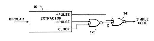
Referring now to Figs. 1 and 2 a ternary, or bipolar,
signal, such as a B3ZS bipolar encoded signal having a strong
clock component and three states -- +1, O, -1 --, is input to
an extractor circuit 10.
;4
- 4 -
The bipolar sign~l may be eparat-d lnto a posltiv-
pulse signal +PU~SE, a negative pul~e ~ignal -PUISE
and a clock oignal CLOCK The ~PULSE ~ignal 18 hlgh
when the bipolar oignal ~tate 16 ~1 and low elsewhere;
the -PULSE signal i~ high wh-n the blpolar ~ignal
Btate 1B -1 and low ~ls-whsr- and the CLOCR lgnal
ha6 a leading edge coincld-nt wlth oach transition of
the bipolar signal Th- IPUISE and CLOCR ignals ~re
combined by a first NOR gat- 12 to produce an
lntermediate signal X that 16 ln turn lnput together
with the -PULSE ~ignal to a ~econd NOR gate 14 The
output o~ th~ ~econd NOR gate 14 16 an NRZ binary
signal, i e , Simple Code that conforms to the rules
of being high when the blpolar ~ignal 1~ +1, low when
the bipolar ~$gnal 1B -1~ and alt-rnating betw-en hlgh
and low when the bipolar ignal 1- zsro
A- hown in Fig 3 th- bipolar ~ignal i~ input to
a lin~ar amplifier 16 having appropriate ~iltering to
comp-n~ate for tr~n~mission 1OB8e~. Th~ output of the
linear a~plifi-r 16 18 lnput to a separator circuit 18
that output~ two binary ~ignals, one representative of
th- Il portlon o~ th- blpolar ~lgnal and th- other
r~pr--entatlv- of the -1 portlon of the bipolar
~ignal Al-o output from th- ~eparator circuit 18 i~
a combin-d ignal that i- input to ynchroni~- a clock
generator 20 Th~ pul--- of th- binary ignal- fro~
th- eparator ¢ircuit 18 hav a pul-- width 1--- than
th- olock cycl- o thae, wh-n co~bin-d, ach l-ading
dg- provid - a trigger pul-- to th- clock g-n-rator
Furth-r to provid- th~ +PULSE and -PULSE ~ignals
havlng full pul-- width- qual to th- Glock cycl-, th
blnary lgnal- fro~ th- eparator circuit 18 ars input
to a pul-e width circuit 22 that i- trigger-d by the
CLOCK ~ignal fro~ th- clock generator 20 The output6
. . - . - - .
- s -
Srom the puls- width elreuit 22 ar- the +PULSE ~nd
-PULSE ignal~ The eloek eyel- of C~OCX ha~ a period
qual to the pul6e wldth of th- lnput blpolar ~ignal,
l e , if ln th~ DS3 format the blpolar ~ignal has a
s strong 22 NNz component, thQ elock fr~qu~ncy $8 44
MHz The outputs of th- clock g~n~rator 20 and the
pulse wldth circuit 22 are input to th- respective NOR
gates 12, 14 a~ described with r 6p~ct to Fig
The output of th- amplifi-r 16, a~ i8 hown in
greater detall ln Flg 4, 1- a c coupled to a bias
network oS resistors Rl, R2 to level sh$ft the bipolar
~ignal Srom z-ro volts d o to a d e level between
the voltage rail6 of the eircuit power upply The
level hift~d bipolar ~ignal is lnput to respeetive
difS-rential comparator- 24, 26 where lt 1~ eompared
re~peetively with a fir~t r fer-nc~ volt~s- REFl,
having a valu~ b-tw--n th~ po~itiv~ rail and the d c
l-v-l, and with a -cond r-f-r-ne~ volt~g- REF2,
having a valu~ b-twe~n th- n-gative ra~l and the d c
level The dlff~rentlal output~ of the eomparator6
24, 26 provide on th- lnvorted output a series of
pulses eorr-sponalng to th- ~1 and -1 value- of the
blpolar lgnal, re~p-etlv-ly Th- noninv~rt~d output6
of the eomparatore 24, 26 ar tl-d togeth-r to provlde
a erl-~ of pul--~ that 1- th- loglcal ~OR~
combinatlon of th- ~1 and -1 valu- pul~-~ o~ th~
blpolar lgnal Th- pul-- wldth- of th- comparator
output- ar- 1--- th-n on- cloek eycl- ln duratlon
Th-r-for- th- lnv-rt-d output- ar input to r--p-ctlv
D-typ- flip-flop- 28, 30 that ar- cloc~-d by th~ CLOCK
lgnal fro~ tho eloek g-n-rator 20 to produce at th-
/Q output- th- ~PULSE an~ -PUISE ignal~,
rosp-ctlv 1y, wlth tha pul--- havlng a wldth gual to
th- p-riod of th- CLOCX lgnal
. . ~
5~
- 6 -
m e po~ltlve pul-- output~ from th- comparator~
24, 26 ~rv- a- yne pul--- for the clocX g n-rator
The po6~tlv- pulsQ outputs are a c coupl-d to ~n
o-c$11ator 32 having tran-l-tor~ Ql, Q2, ~n
5 approprlate r-sl~tive bl~slng networ~, and an LC t~nk
clrcuit ln the eoll-ctor cireult of Ql The lne w~ve
output from th- oscillator 32 is a e couplod to a
thlrd co~parator 36 for eonv-rsion lnto th- CLOCK
~lgnal A third referenc- voltage REF3, havlng a
value approxlmately qual to the zero crosslng value
oS the sine wave, provldes a posltive pul~e at the
output for the po~ltlve portlon of the slne wave input
having a pul~Q wldth gual to ons-half the perlod of
the CLOCX lgnal The resultlnq CLOCK ~lgnal from the
clock g-nerator 20 1~ eombln-d wlth the +PULSE and
-PULSE lgnal~ by NOR gat-~ 12, 14 a~ de-crlb-d
abov- Th- resultlng 81~ple Cod- output i~ lnput to
an output buff-r ampllfl-r 38 to provid- a
diff-rentlal 81apl- Code output for transals~lon
At th- recelvlng nd a deeoder 40 as hown ln Flg
S has an lnput buffer ampllfl-r 42 whlch receives the
tran~mlttod 81~pl- Cod- Th- output of the ampllfler
42 18 lnput to a clock generator 44 to recov~r the
CLOCX lgnal ~ro~ the 8iapl- Cod-, and al-o 18 lnput
to a d-cod- clreult ~6 Thr-e phases of th- CLOCX
lgnal -- 90, 270 and 360 -- fro~ the elocX
generator 44 ar- input to th- d-cod- elreult 46, and
th- d-cod clreult output- a po-ltlv pul-- lgnal and
a n-gatlv pul-- lgnai Th po~ltlv and n gatlv
pul~- lgnal- fro~ th- d-cod- elreult ~6 ar- eoabln-d
~la a r-sl-tlv uualng n-twork at th lnput of an
output buff r ~nplifl-r 48 to produc- a bipolar ignal
that i- a r produotlon of th- blpolar lqnal lnput to
th- tran-altt-r o~ Flg 3
- 7 -
Th~ differ-nti~l Simpl- Cod- fro~ th- tran~mitt-r
output buffQr ~pll~l-r 38 1- lnput to th- lnput
buffer a~pllfi-r ~2 at the r-c-lv-r 40 a~ hown ln
Flg6 5 and 6 Th- diff-r-ntLal ~impl~ Cod- output
from th~ lnput amplifl-r ~2 1- a o coupl-d to an
oscillator 50 havlng tran~istor- Q3, Q4, a r-sistlve
blasing nQtwork and an LC tank clrcult 52 ln the
! collector circuit of Q3 ~h~ dlff~rQntial Simpl- Code
¦ input to th~ clock generator 44 ~erv~s to ~ynchronize
i 10 the oscillator 50 Th- ~inusoidal output of the
06cillator 50 is a c coupled to an oscillator buffer
amplifi~r 54 having a transistor Q5 with appropriate
biasing r-sistors and an output d~lay network 56 The
delay-d sinusoidal clock from th~ delay network 56 i8
input to a fourth comp~rator 58 while an undelay~d
~inusoid~l clock 1- a c coupl-d to a fifth comp~rator
Th- comparator- 58, 60 hav- a fourth rQfer-nce
voltag- REF4 a~ a compari-on input to convert the
~inu-oldal clock- lnto guar- wav- clocks Th- output
f the fourth comparator 58 1- a diff~r-ntial delayed
CLOCK lgnal provlding th~ 90 and 270 phas~s,
and th- output of th- fifth comparator 60 18 an
und-layed, or 360 pha-~, CLOCX ~ignal
One of th~ 81mpl- Cod- output~ from the lnput
ampllfl-r 42 1- lnput to a palr of D-typ- fllp-flop~
; 62, 64 ln th d-cod- clrcult ~6 On- of th~
fllp-flop- i- clock-d by th 90 CLOCX ~lgnal and
th- oth-r 1~ clock d ~y th 270 CLOCX lgnal fro~
th- d-lay ¢omparator S8 T~- Q output~ of th- palr of
fllp-flop- ar lnput to a ~-cond palr of D-typ~
fllp-flop- 66, 68 Th ~-cond pair of fllp-flop- ar-
cloc~ad ~lnultan-ou-ly by th- und-lay~d CLOCX ~lgnal
from th comparator 60 The /Q output of on-
~llp-flop 66 of the -cond palr 1~ lnput to a NAND
g~5~
gate 70 and the Q output of the other flip-flop 6~ of the
second pair is input to an AND gate 72. The other input to
the NAND gate 70 and to the AND gate 72 is the 90 CLOCK
signal. The NAND gate 70 outputs a negative pulse signal
corresponding to the -PULSE signal at the encoder, and the AND
gate 72 outputs a positive pulse signal corresponding to the
+PULSE signal at the encoder. The outputs of the NAND gate 70
and the AND gate 72 are input to the resistive summing network
at the input to the output buffer amplifier 48, which
preferably is a multifunction amplifier that combines the
positive and negative pulse binary signals via a resistive
summing network at the input and provides appropriate
buffering and impedance matching. The output of the
output amplifier 48 is the reconstructed bipolar signal.
In operation the delayed CLOCK signal from the delay
comparator 58 as applied to the first set of flip-flops
62, 64 samples the Simple Code input twice per CLOCK
period. The delay assures that the sampling occurs after
the pulse transition edges of the Simple Code to eliminate
any ambiguities. If the value of the Simple Code during
a CLOCK period is the same for both flip-flops 62, 64,
then the output value is either negative or positive
depending upon whether the Simple Code was low or high.
If the value of the Simple Code alternates during the
CLOCK period, then the output values of the flip-flops 62,
64 will be different, indicating a zero value. The data
from the flip-flops 62, 64 is transferred to the second
pair of flip-flops 66, 68 by the next CLOCK signal from
L~
~ ~ 9 4
¢o~parator 60, ~g~in to avold any ambigultl-- that
would be caused lf the tran-f-r occurred
lmultaneously with th- dhanqe of tate of the
preceding flip-flop pair The r-6ultinq po-itive and
negative pulse ~ignal~ from the ~econd pair of
flip-flops 66, 68 are combined by the output amplifier
48 to produce the ternary ~ignal accordlng to the
above described scheme
Thus the present invention providQs a Simple Code
encoder/decoder for converting a ternary, or bipolar,
~ignal into a binary lgnal tor digltal processing by
combining a +PULSE ignal d-rlved from the +l value of
the bipolar ignal with a -PULSE ~ignal derived from
the -1 valu- of the bipolar ~ignal and a CLOCK signal
derived from the bipolar ~ignal ~uch that the binary
Simple Code is high for +1 values, low for -1 values
and alternates high/low for ~ero values