Note: Descriptions are shown in the official language in which they were submitted.
lZ89280
01 This invention relates in general to
02 telephone systems, and more particularly to a central
03 office line card with distributed signaling voltages.
04 In a telephone central office various
05 types of signaling voltages are required to be
06 generated for transmission to di~ferent types of
07 telephones connected thereto via well known balanced
08 tip and ring leads. For example, in North America, a
09 standard telephone requires a 90 volts RMS ringing
signal voltage at 20 hertz applied to one of either
11 the ring or tip lead. Telephones which are connected
12 in parallel forming a party line, require specific
13 identifying DC voltages superimposed on the ringing
14 signal voltage in order to identify particular ones of
the telephones connected in the party line.
16 Furthermore, coin operated telephones typically
17 require + 130 volt DC control voltage for operating a
18 solenoid to direct a coin to one of either the
19 collection box or the customer, depending on the
polarity of the control voltage. Also, + 48 volt test
21 voltages are required for coin operated telephone
22 lines in order to detect a presence of a coin.
23 According to prior art systems, ringing
24 signal voltages as well as the required DC signaling
voltages for party lines and coin operated telephones
26 were generated by one or more signal generators in the
27 central office and applied via respective relays to
28 the tip or ring lead of a subscriber line interface
29 i circuit disposed on a line card. Thus, a relay was
associated with each of the signaling voltages applied
31 to each of the telephone lines connected to the
32 central office. This resulted in a large number of
33 relays, and consequently great expense and circuit
34 board complexity.
An improved distributed signaling system
36 was utilized by Northern Telecom on the DMS 100~
lZ89280
ol - 2 -
02 exchange. According to the Northern Telecom system a
03 sophisticated signal generator is used for generating all
04 of the required signaling voltages and applies the
05 voltages in time division multiplex fashion to a common
06 signaling bus which extends along the exchange backplane,
07 and is connected to individual trunk cards of the
08 exchange. Thus, the remote signal generator transmits
09 the various signaling voltages such as +130, -130 volts,
90 volts RMS, etc., in respective time slots onto the
11 signaling bus for reception by a plurality of subscriber
12 line interface circuits each including circuitry for
13 demultiplexing the time divided signals.
14 A fundamental disadvantage of the Northern
Telecom system is that each of the subscriber line
16 interface circuits which requires a particular
17 signaling voltage must wait until that voltage is
18 available in the time division multiplex sequence.
19 Thus, with many line circuits connected to a bus (eg.
typically more than 100 line circuits in a central
21 office configuration), the single generator in the
22 Northern Telecom system is incapable of supplying all
23 of the required signaling voltages to each of the line
24 circuits needing them at a particular instant in
time.
26 Furthermore, the common signal generator
27 in the Northern Telecom system must be sophisticated
28 enough to provide all of the voltages required within
29 i the central office exchange. In other words, complex
and expensive circuitry is required to generate all of
31 the required signaling voltages in recurring sequence,
32 even though there may only be a single coin operated
33 telephone or party line configuration within the system
34 which would require the special associated signaling
35 voltage.
36 According to the present invention, a
37 central office line card is provided which is comprised
38 of a common signaling bus connected to a plurality of
1289280
01 ~ 3 ~
02 subscriber line interface circuit via respective
03 relays. The signaling bus is connected to a remote
04 ringing signal generator by a relay, for receiving a
05 90 volts RMS 20 Hertz ringing signal which is common
06 to all telephones connected to the central office.
07 A receptacle is provided connected to the signaling
08 bus on the line card via a further relay, for
09 receiving a removable module for generating additional
signaling vol~ages such as those required for
11 operating coin telephones or party line telephone
12 sets.
13 By utilizing a common signaling bus on the
14 line card to distribute different signaling voltages,
the requirement of prior art systems for multiple
16 relays per line for signaling voltage, is avoided.
17 The module is inserted within the receptacle only in
18 the event that the particular signaling voltages are
19 required on the line card. Thus, in contrast with the
expensive and complex time division multiplex signal
21 generating circuitry of Northern Telecom, according to
22 the present invention a small, inexpensive module can
23 be added to the line card for generating specialized
24 signaling voltages (eg. coin telephone or party line
voltages).
26 For example, in a central office with 400
27 lines, as few as three lines may be connected to coin
28 operated telephones. Thus, according to the present
29 invention only one line card would require a
specialized signaling module to be connected thereto,
31 the remaining line cards supporting an empty
32 receptacle and being connected only to the standard
33 ringing signal generator.
34 Moreover, ringing signal voltage as well
as any required specialized signaling voltages are
36 applied to the telephone lines immediately according
37 to the present invention, such that the prior art
38 disadvantage of being required to wait for an
39 available signaling voltage time slot, is overcome.
~289280
01 - 4 -
02 In general, according to the present
03 invention there is provided for use in a telephone
04 system having a plurality of remote telephones
05 connected thereto, and including a ringing generator
06 for generating ringing signals for application to the
07 remote telephones; a line card circuit for
08 distributing and applying the ringing signals and
09 predetermined control signals to the remote
telephones, comprised of a plurality of subscriber
11 line interface circuits for connection to respective
12 ones of the telephones via two-wire telephone lines,
13 a signalling bus connected via first relay circuitry
14 to respective ones of the telephone lines, and via
second relay circuitry to the ringing generator, a
16 removable signal module for generating the
17 predetermined control signals, a receptacle for
18 receiving the signal module comprised of one or more
19 terminals for connection to the signal module via
third relay circuitry to the bus, and circuitry for
21 selectively actuating the first, second and third
22 relay circuitry for selectively connecting one of
23 either the ringing generator or the signal module to
24 predetermined ones of the telephone lines via the bus,
whereby the ringing signals and the predetermined
26 control signals are selectively distributed and
27 applied to respective ones of the telephones connected
28 to the two-wire telephone lines.
29 A better understanding of the present
invention will be obtained with reference to the
31 detailed description below in conjunction with the
32 following drawings in which:
33 Figure 1 is a block diagram showing a
34 line card in accordance with the present invention in
its most general form,
36 Figure 2 is a schematic diagram
37 illustrating relay circuitry in the line card of
12~9280
01 ~ 5 ~
02 Figure 1, and
03 Figure 3 is a schematic diagram of a coin
04 signaling voltage module in accordance with the
05 preferred embodiment of present invention.
06 Turning to Figure 1, a central office
07 line card 1 is shown comprised of a plurality of
08 subscriber line interface circuits 3, 57 connected
09 via respective telephone lines 15, 17... 19 to remote
telephones 9, 11... 13. Each of the telephone lines
11 15, 17... 19 is also connected via respective relays
12 KB, to a common signaling bus 21.
13 A remote ringing signaling generator 23 is
14 disposed within the central office circuitry remote
from the line card 1, and is configured for generating
16 well known 90 volt RMS 20 Hertz ringing signal
17 voltage. The circuitry of ringing generator 23 does
18 not form part of the present invention, and is very
19 well known in the art. Ringing signal voltage ls
transmitted from generator 23 and applied to a central
21 office backplane bus 25 connected to the line card 1
22 via a terminal 27, and to the common signal bus 21 via
23 a further relay K3.
24 Although not shown, typically a plurality
of line cards such as line card 1 would be provided in
26 the central office, each connected to backplane bus 25
27 and each comprised of a plurality of subscriber line
28 interface circuits. For example, in a central office
29 with 400 lines, 67 such line cards would be required,
each including six subscriber line interface circuits.
31 Also incorporated within the line card 1
32 is a receptacle shown diagramatically via additional
33 terminal 31, for receiving an optional removable
34 signal module 33 for generating special signaling
voltages such as those required for operating coin
36 telephone sets and party line telephone sets.
37 A relay control circuit 35 is provided
38 for generating control signals to activate relays KB,
i2~39280
01 - 6 -
02 K3 and R5. Thus, in operation, relay control circuit 35
03 generates signals for connecting one of either signal
04 module 33 or ringing generator 23 to the common signal
05 bus 21 via relays K5 and K3. Next, predetermined ones of
06 the telephone lines 15, 17... 19 connected to telephone
07 sets 9, 11... 13 are connected to the signaling bus for
08 receiving one of either ringing signal from generator 23
09 or special signaling voltages from module 33, via the KB
relays.
11 Thus, in a typical central office exchange,
12 a majority of the plurality of line cards 1 would not
13 include the signal module 33, and would be provided only
14 with an empty receptacle 31. However, any party line or
coin telephones requiring special signal voltages would
16 be connected to a line card of the exchange which
17 includes an appropriate signal module 33. In this way,
18 the large majority of line cards are provided with
19 minimal circuitry for connecting individual subscriber
line interface circuits to the PCM highway 15, and common
21 signal bus 21, and for connecting the remote ringing
22 generator to the bus. Yet only a small number of line
23 cards are provided with the special signal module 33 for
24 generating coin telephone and party line signal
25 voltages.
26 Thus, as discussed above, each line card
27 includes a minimum of expensive and complex circuitry,
28 requiring only a small number of relays, while, each of
29 i the telephones is provided with instantaneous signaling
voltages, without being required to wait for the
31 signaling voltage to appear periodically in a time
32 devided multiplex sequence, as in the prior art.
33 Turning to Figure 2, a schematic diagram
34 of a preferred embodiment of the line card of the
present invention is shown connected to TIP and RING
36 leads of a predetermined one of the subscriber
1289280
01 _ 7 _
02 line interface circuits, such as circuit 3 in Figure
03 1, via a pair of relays KB. Ringing signal from the
04 remote ringing generator 23 (Figure 1) is received via
05 terminal 27 and applied to the common signal bus 21
06 via relay K3. Signals from the removable signal module
07 33 (Figure 1) are received via receptacle 31, as
08 discussed in greater detail below.
09 A further test signal MFRE is received via
additional terminal 41 and is applied via relay K4 to
11 the signal bus 21.
12 Signals appearing on bus 21 may be applied
13 in various modes to the TIP and RING lead. For
14 example, signaling voltage may be applied to both the
tip and ring leads by closing the KB relays as well as
16 the K2 relay. This is known in the art as simplex
17 signaling. Alternatively, the signaling voltage can
18 be reversed via reversal relays K8 in order to
19 accomplish signaling polarity reversal without
requiring a reversal in the battery feed polarity.
21 The subscriber line interface circuit 3 is
22 shown with unidirectional transmit and receive leads
23 carrying respective transmit and receive signals Vx
24 and VR to and from a codec 45 which converts analog
signals on the TIP and RING lead to digital signals
26 carried by input and output PCM leads PCMI and PCM0 to
27 and from PCM highway 15, in a well known manner.
28 Normally, the RING lead is connected via
29 relay KB to the remote ringing generator 23 (Figure 1)
via relays K8 and K3, with the TIP lead being
31 connected via relays KB, K8, Kl and K2 to the ground
32 return terminal RET.
33 The test voltages MFRE received on
34 terminal 41 are applied via relay K4 differentially to
inverting and non-inverting inputs of a threshold
36 detection circuit 43, for detecting presence of coins
37 in coin operated telephones, or determining which
~Z89i~
01 - 8 -
02 member of a party line is making a toll call. The
03 threshold detection circuit 43 and operation thereof
04 does not form part of the present invention, and is
05 discussed herein for the purpose of completeness only.
06 The external signal module 33 (Figure 1)
07 is plugged into receptacle 31 which is comprised of a
08 plurality of terminals for receiving signal voltages
09 such as -130 volts, +13~ volts, +48 volts and -48
volts. The +130 volt and -130 volt signals are
11 selected by means of a relay K7 and applied to the
12 signal bus 21 via a relay K5. Similarly the +48 volt
13 and -48 volt signals are selected via a relay K6 and
14 applied to signal bus 21 via the K5 relay. The +48 volt
and -48 volt signals may be applied to signal bus 21
16 either directly through relay K2 or via a current
17 limiting resister R2. ~~
18 The relays KB and Kl-K8 are controlled via
19 a relay control circuit 35 comprised of a plurality of
inverters 47-63 having respective outputs thereof
21 connected to energizing coiLs for the relays Ks,
22 Kl-K8, each of the relay coils also being connected to
23 a source of +12 volt relay energizing current.
24 In operation, the signal bus 21 is
connected to the TIP and RING leads via the KB relays
26 in response to generation of a control signal
27 designated SIGNAL by a remote peripheral controller
28 (not shown) of the telephone system. The control
29 Bignal i8 applied to the input of inverter 47 such that
the output thereof goes to a logic low (ie. ground)
31 level causing the current to flow from the +12 volt
32 source through the KB energizing relay coil to ground.
33 The signal bus 21 is connected to the TIP and RING leads
34 for receiving various different modes of signaling. For
example, signaling voltages on the bus 21 may be applied
36 to both of the tip and ring leads by closing the K2
37 relay in order to provide simplex signaling. This is
1289280
01 ~ 9 ~
02 accomplished by the peripheral controller generating
03 an SMPLX control signal for application to the input
04 of the inver~er 51, causing energizing current to flow
05 through the K2 relay coil. Alternatively, signaling
06 reversal may be accomplished without battery feed
07 reversal by actuating relay K8. This is done by the
08 peripheral controller generating a REVSIG control
09 signal for application to transistor Ql via current
limiting resistor R3. The emitte-r of transistor Ql is
11 connected to circuit ground DG as well as to the
12 collector of transistor Ql via a diode Dl.
13 The Kl relay is actuated to provide
14 battery return RET to the TIP lead. This is
accomplished by means of the peripheral controller
16 generating a RET ON control signal to the input of
17 inverter 49, causing energizing current to flow
18 through the Kl relay coil.
19 Ringing signal is received from the remote
ringing generator 23 (Figure 1) via backplane bus 25
21 and terminal 27 of the trunk card and applied to
22 the signal bus 21 via normally closed relay K3.
23 However, upon actuating relays K3 and K4, remote
24 signaling voltages may be received from the signal
module 33. In particular, the peripheral controller
26 generates one or more control signals designated MFR,
27 COIN 1, ANI 2, ANI 1 or COIN 2 for energizing the K3
28 relay, and generates one or more of the COIN 1, ANI 2,
29 i ANI 1 or COIN 2 signals for energizing the K4 relay.
Furthermore, upon energizing the K4 relay,
31 current flows from the base of PNP transistor Q2
32 through resister R4 to ground, thereby enabling
33 transistor Q3 such that the voltage on a collector
34 terminal thereof rises to +12 volts. The collector
terminal of transistor Q3 is connected to a COINEN
36 enable input of signal module 33, as discussed in
37 greater detail below with reference to Figure 3.
1289280
01 - 10 -
02 As discussed above, one of either the
03 -130 volt of +130 volt coin signal voltaqes may be
04 selected by enabling or disabling the K7 relay by
05 alternately generating logic high or logic low level
06 COIN 2 control signals, and the K5 relay may be
07 enabled or disabled by generating logic high and logic
08 low COIN 1 and COIN 2 control signals. Similarly, one
09 of either the +48 volt or -48 volt signal voltages may
be selected in response to selectively energizing the
11 K6 relay by means of generating logic high or logic
12 low ANI 1 control signals. For example, in order to
13 apply a +48 volt party line signal voltage to the RING
14 lead, the K6, K4, K3 and KB relays are energized. The
+48 volt control signal may be applied with reverse
16 battery by means of energizing the K8 relay.
17 Alternatively, the +48 volt signal may be applied to
18 both the TIP and RI~G leads by enabling the K2 relay,
19 in which case the +48 volt control signal bypasses
damping resistor R2.
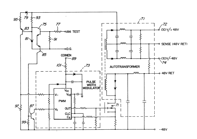
21 Turning to Figure 3, a schematic diagram
22 is illustrated showing signal module 33 configured as
23 a coin telephone module. Alternatively, the signal
24 module 33 may contain circuitry for generating message
waiting lamp control signals, party line selective
26 ringing signals, etc.
27 In general, the circuit of Figure 3
28 illustrates a fly-back power supply utilizing an auto
29 ; transformer Tl, as opposed to an isolated transformer
such as used in standard implementations. A main
31 power switch 71 (eg. a power MOSFET) is driven by a
32 pulse width modulator 73 for producing +130 volt/+
33 volt, -130 volt/-48 volt, and 48 volt control signals
34 referenced to a +48 volt return (ie. SENSE). The
control signals are selectable between +130 volt, -130
36 volt and +48 volt, -48 volt by means of a further
37 control signal ANI TEST generated by the peripheral
~289280
0 1
02 controller (not shown) and applied to the base of
03 transistor 75 via current limiting resistor 77. In
04 particular, in response to a logic low level ANI TEST
05 signal applied to the base of transistor 75, the
06 transistor 75 remains off such that the voltage drop
07 between the terminal 72 and the digital ground
08 terminal (DG) remains at +130 volts, due to the
09 combined +130 volt voltage drop of zener diodes 79 and
81. In particular, diode 79 provides a 48 volt drop
11 while diode 81 provides an 82 volt drop. In the event
12 that the voltage at terminal 72 rises above +130
13 volts, transistor 83 begins conducting, thereby
14 inhibiting the pulse width modulator 73.
In order to produce +48 volt and -48 volt
16 signals on the terminals 72 and 74, the peripheral
17 controller generates a logic high level ANI TEST
18 signal for application to transistor 75. In response,
19 transistor 75 conducts, thereby bypassing zener diode
81 such that the voltage appearing at terminal 72 is
21 +48 volts, appearing across zener diode 79, while the
22 voltage at terminal 74 is -48 volts due to the reverse
23 polarity transformer coupling of auto-transformer Tl.
24 Additional transistors 85 and 87 provide
current limiting protection of the auto transformer
26 power supply. For example, in the event that the +130
27 volt and -130 volt output is selected, the current
28 limiting is set at approximately 50 milliamps, while
29 i in the event that the output is selected for +48 volts
and -48 volts, the current limit is set to
31 approximately to 15 milliamps in response to enabling
32 transistors 85 and 87, thereby reducing the voltage
33 applied to the Vc input of the PWM circuit within
34 pulse width modulator 73 from 3 volts down to
approximately +1 volt.
36 The coin module power supply of Figure 3
37 switches at a high frequency rate of approximately .5
~289Z80
01 - 12 -
02 megahertz.
03 As discussed above, the COINEN signal is
04 generated in response enabling the K4 relay for
05 receiving signals from the remote signal module 33.
06 The COINE~ signal is applied via terminal 89 to the
07 pulse width modulator 73 for enabling the PWM circuit
08 via power input terminal Vcc Thus, the signal
09 module 33 draws power only in the event that relay K4
is energized, thereby reducing power consumption
11 within the system when the signal module 33 is not in
12 use.
13 Additional circuitry such as resistors 91,
14 93, 95, 97, 99 and 101 are provided for current
limiting and buffsring, in a well known manner.
16 The +130 volt signal is utilized to
17 collect a coin in a remote coin telephone connected to
18 the line card 1I while the -130 volt contro signal
19 causes the coin to be released. Similarly, the +48
volt and the -48 volt signals are utilized for
21 providing party line identification detection within a
22 party line systeml in a well known manner.
23 In summaryl according to the present
24 invention a line card is provided for use in a central
office telephone system wherein a common bus is
26 provided on the card for distributing signaling
27 voltages such as message waitingl coin controll testl
28 party line controll etc. By incorporating the common
29 signaling bus on the line card itself as opposed to
utilizing a backplane bus as in prior art system
31 smaller granularity is provided over prior art
32 systems.
33 Alsol circuity is provided in the present
34 invention for reversingl opening or closing the
signaling applied to the tip and ring leadsl without
36 requiring battery feed reversal, etc.l as in the prior
37 art. Moreover, the provision of external signaling
38 voltage on a pay-as-you-go basis alleviates the prior
128928(3
01 - 13 -
02 art requirement for sophisticated and expensive
03 centralized signal generators. In addition, the
04 circuitry for connecting the external signal module to
05 the common line card signal bus prevents the signal
06 module from drawing power when not in use.
07 A person understanding the present
08 invention may conceive of other embodiments or
09 variation therein. All such embodiments or variations
10 are beleived to be within the sphere and scope of the
11 present invention as defined in the claims appended
12 hereto.
: ~ `
. '