Language selection

Search

Patent 1289678 Summary

Third-party information liability

Some of the information on this Web page has been provided by external sources. The Government of Canada is not responsible for the accuracy, reliability or currency of the information supplied by external sources. Users wishing to rely upon this information should consult directly with the source of the information. Content provided by external sources is not subject to official languages, privacy and accessibility requirements.

Claims and Abstract availability

Any discrepancies in the text and image of the Claims and Abstract are due to differing posting times. Text of the Claims and Abstract are posted:

  • At the time the application is open to public inspection;
  • At the time of issue of the patent (grant).
(12) Patent: (11) CA 1289678
(21) Application Number: 546343
(54) English Title: APPARATUS FOR ELECTRICALLY TESTING PRINTED CIRCUIT BOARDS HAVING CONTACT PADS IN AN EXTREMELY FINE GRIP
(54) French Title: APPAREIL POUR LA VERIFICATION ELECTRIQUE DE CIRCUITS IMPRIMES A PASTILLES DE CONTACT FIXEES RIGIDEMENT
Status: Expired
Bibliographic Data
(52) Canadian Patent Classification (CPC):
  • 356/2
(51) International Patent Classification (IPC):
  • G01R 1/073 (2006.01)
  • H01R 11/18 (2006.01)
(72) Inventors :
  • DRILLER, HUBERT (Germany)
  • MANG, PAUL (Germany)
(73) Owners :
  • MANIA TECHNOLOGIE AG (Germany)
(71) Applicants :
(74) Agent: RICHES, MCKENZIE & HERBERT LLP
(74) Associate agent:
(45) Issued: 1991-09-24
(22) Filed Date: 1987-09-08
Availability of licence: N/A
(25) Language of filing: English

Patent Cooperation Treaty (PCT): No

(30) Application Priority Data:
Application No. Country/Territory Date
P 36 30 548.0 Germany 1986-09-08

Abstracts

English Abstract


ABSTRACT OF THE DISCLOSURE
A circuit board testing apparatus includes a
plurality of contact elements located in a contact array
plane. The contact elements are connected to an electronic
control and test structure and during testing are connected
through longitudinally rigid test pins to contact portions
of a connection carrier or circuit board to be tested. The
contact elements are mounted to yield resiliently and are
supported against the contact pressure applied during
testing. The contact elements are in the form of
electrically conductive compression springs located and
guided directly in bores in a spring contact array body
formed of an electrically insulating material. The rigid
test pins seat directly on the compression springs.


Claims

Note: Claims are shown in the official language in which they were submitted.


The embodiments of the invention in which an
exclusive property or privilege is claimed are defined as
follows:
1. A contact element assembly for use in a printed
circuit board testing apparatus to provide electric
connection between electronic control and test means of
the testing apparatus and, through longitudinal test pins,
contact positions of a connection carrier or circuit board
to be tested, said assembly comprising:
a spring contact array body formed of an
electrically insulating material and having therethrough a
plurality of bores;
a plurality of electrically conductive
compression springs, each said spring being located in a
respective said bore, each said spring having at a first
end thereof means for achieving electrical contact with a
longitudinal test pin of the testing apparatus and for
centering and guiding the respective longitudinal test
pin, at a second end thereof means for achieving
electrical connection with the electronic control and test
means of the testing apparatus, and between said first and
second ends thereof a resiliently yieldable portion;
the relative dimensions of each said bore and the
respective said spring being such that, upon application
to said spring by the respective longitudinal test pin of


14


a testing contact pressure, said resiliently yieldable
portion of said spring engages the surface of said spring
contact array body defining said bore; and
a driver card supporting electronic control
components, a contact array plug on one end of said driver
card, said contact array plug including means for making
direct electric contact with said means at said second
ends of said compression springs and means for
transmitting contact pressure to support elements of the
circuit board testing apparatus, said electric contact
means comprising contact pins extending from said contact
array plug to be introduced into said bores in said spring
contact array body.


2. An assembly as claimed in claim 1, wherein said
spring contact array body is made of a ceramic or a
plastic material.


3. An assembly as claimed in claim 1, wherein said
spring contact array body is formed of a plurality of
segments assembled in array form.


4. An assembly as claimed in claim 1, further
comprising a plurality of longitudinally rigid test pins
extending into respective said bores and electrically
connected to first ends of respective said spring therein.


5. An assembly as claimed in claim 4, wherein said
test pins are seated directly on said first ends of said
respective springs.


6. An assembly as claimed in claim 1, wherein said
means at at least one of said first and second ends of
said compression spring is formed by contiguous turns of
incrementally and/or gradually reduced coil diameter to
form a pin-like shape.


7. An assembly as claimed in claim 1, wherein said
means at at least one of said first and second ends of
said compression spring is formed by contiguous turns of
incrementally and/or gradually reduced coil diameter to
form a tapered shape.


8. An assembly as claimed in claim 1, wherein said
means at at least one of said first and second ends of
said compression spring is formed by contiguous turns of
first decreasing and then increasing diameter to define a
portion internally tapered for directly receiving an end
of a test or contact pin.


16


9. An assembly as claimed in claim 1, wherein each
said compression spring has at least one end portion
thereof formed by contiguous turns having maximum diameter
for stable guidance inside the respective said bore in
said spring contact array body.


10. An assembly as claimed in claim 1, wherein each
said compression spring includes contiguous turns
interconnected mechanically by means such as a coating of
metal plated thereon.


11. An assembly as claimed in claim 1, wherein end
portions of said compression springs are coated with a
contact material for improved electrical contact.


12. An assembly as claimed In claim 1, wherein said
means at said second end of each said compression spring
includes a resilient contact tongue extending
longitudinally from said compression spring for direct
engagement with contact areas of said driver card
supporting said electronic control components.


13. An assembly as claimed in claim 12, wherein said
resilient contact tongues extend through respective bores
in said contact array plug.

17


14. A contact assembly comprising:
a plurality of contact elements assemblies for
use in a printed circuit board testing apparatus to
provide electric connection between electronic control and
test means of the testing apparatus and, through
longitudinal test pins, contact positions of a connection
carrier or circuit board to be tested, each said assembly
comprising:
a spring contact array body formed of an
electrically insulating material and having therethrough a
plurality of bores;
a plurality of electrically conductive
compression springs, each said spring being located in a
respective said bore, each spring having at a first end
thereof means for achieving electrical contact with a
longitudinal test pin of the testing apparatus and for
centering and guiding the respective longitudinal test pin
at a second end thereof means for achieving electrical
connection with the electronic control and test means of
the testing apparatus, and between said first and second
ends thereof a resiliently yieldable portion; and
the relative dimensions of each said bore and the
respective said spring being such that, upon application
to said spring by the respective longitudinal test pin of


18


a testing contact pressure, said resiliently yieldable
portion of said spring engages the surface of said spring
contact array body defining said bore;
said spring contact array bodies of said
plurality of assemblies having different densities of said
compression springs therein; and
a plurality of respective electronic control
components and driver cards supporting respective contact
array plugs having means for making direct electric
contact with said means at said second ends of said
compression springs of said plurality of spring contact
array bodies, said plurality of spring contact array
bodies being exchangeably connectable to different of said
plurality of contact array plugs.


15. An assembly as claimed in claim 14, wherein said
spring contact array bodies are made of a ceramic or a
plastic material.


16. An assembly as claimed in claim 14, wherein each
said spring contact array body is formed of a plurality of
segments assembled in array form.


17. An assembly as claimed in claim 14, further
comprising a plurality of longitudinally rigid test pins


19


extending into respective said bores and electrically
connected to first ends of respective said springs
therein.

18. An assembly as claimed in claim 17, wherein said
test pins are seated directly on said first ends of said
respective springs.

19. An assembly as claimed in claim 16, wherein said
means at at least one of said first and second ends of
said compression spring is formed by contiguous turns of
incrementally and/or gradually reduced coil diameter to
form a pin-like shape.

20. An assembly as claimed in claim 16, wherein said
means at at least one of said first and second ends of
said compression spring is formed by contiguous turns of
incrementally and/or gradually reduced coil diameter to
form a tapered shape.

21. An assembly as claimed in claim 14, wherein said
means at at least one of said first and second ends of
said compression spring is formed by contiguous turns of
first decreasing and then increasing diameter to define a
portion internally tapered for directly receiving an end
of a test or contact pin.


22. An assembly as claimed in claim 14, wherein each
said compression spring has at at least one end portion
thereof formed by contiguous turns having maximum diameter
for stable guidance inside the respective said bore in
said spring contact array body.


23. An assembly as claimed in claim 14, wherein each
said compression spring includes contiguous turns
interconnected mechanically by means such as a coating of
metal plated thereon.


24. An assembly as claimed in claim 14, wherein end
portion of said compression springs are coated with a
contact material for improved electrical contact.


25. An assembly as claimed in claim 14, wherein said
electric contact means of each said contact array plug
comprise contact pins extending from said contact array
plug to be introduced into said bores in said spring
contact array bodies.


26. An assembly as claimed in claim 14, wherein said
means at said second end of each said compression spring
includes a resilient contact tongue extending


21


longitudinally from said compression spring for direct
engagement with contact area of one of said driver cards
supporting said electronic control components.

27. An assembly as claimed in claim 26, wherein said
resilient contact tongues extend through respective bores
in said contact array plugs.

28. A contact element assembly for use in a printed
circuit board testing apparatus to provide electric
connection between electronic control and test means of
the testing apparatus and, through longitudinal test pins,
contact positions of a connection carrier or circuit board
to be tested, said assembly comprising:
a spring contact array body form substantially of
an electrically insulating material and having
therethrough a plurality of bores;
a plurality of electrically conductive
compression springs, each said spring being located in a
respective said bore, each said spring having at a first
end thereof means for achieving electrical contact with a
longitudinally test pin of the testing apparatus and for
centering and guiding the respective longitudinal test
pin, at a second end thereof means for achieving
electrical connection with the electronic control and test


22


means of the testing apparatus, and between said first and
second ends thereof a resiliently yieldably portion;
a driver card supporting electronic control
components and having contact areas; and
said means at said second end of each said
compression spring including a resilient contact tongue
extending longitudinally from said compression spring and
directly engaging with a said contact area of said driver
card supporting said electronic control components.

29. An assembly as claimed in claim 28, wherein said
spring contact array body is substantially made of a
ceramic or a plastic material.

30. An assembly as claimed in claim 28, wherein said
spring contact array body is formed of a plurality of
segments assembled in array form.

31. An assembly as claimed in claim 28, further
comprising a plurality of longitudinally rigid test pins
extending into respective said bores and electrically
connected to first ends of respective said springs
therein.


23


32. An assembly as claimed in claim 31, wherein said
test pins are seated directly on said first ends of said
respective springs.

33. An assembly as claimed in claim 28, wherein said
means at said first end of said compression spring is
formed by contiguous turns of incrementally and/or
gradually reduced coil diameter to form a pin-like shape.

34. An assembly as claimed in claim 28, wherein said
means at said first end of said compression spring is
formed by contiguous turns of incrementally and/or
gradually reduced coil diameter to form a tapered shape.

35. An assembly as claimed in claim 28, wherein said
means at said first end of said compression spring is
formed by contiguous turns of first decreasing and then
increasing diameter to define a portion internally tapered
for directly receiving an end of a test pin.

36. An assembly as claimed in claim 28, wherein each
said compression spring has at least one end portion
thereof formed by contiguous turns having maximum diameter
for stable guidance inside the respective said bore in
said spring contact array body.


24


37. An assembly as claimed in claim 28, wherein each
said compression spring includes contiguous turns
interconnected mechanically by means such as a coating of
metal plated thereon.

38. An assembly as claimed in claim 28, wherein end
portions of said compression springs are coated with a
contact material for improved electrical contact.

39. An assembly as claimed in claim 28, further
comprising a contact array plug at one end of said driver
card, and wherein said resilient contact tongues extend
through respective bores in said contact array plug.

40. An assembly as claimed in claim 28, wherein the
relative dimensions of each said bore and the respective
said spring are such that, upon application to said spring
by the respective longitudinal test pin of a testing
contact pressure, said resiliently yieldable portion of
said spring engages the surface of said spring contact
array body defining said bore.


41. A contact array comprising:
a plurality of contact element assemblies for use
in a printed circuit board testing apparatus to provide
electric connection between electronic control and test
means of the testing apparatus and, through longitudinal
test pins, contact positions of a connection carrier or
circuit board to be tested, each said assembly comprising:
a spring contact array body formed
substantially of an electrically insulating material and
having therethrough a plurality of bores; and
a plurality of electrically conductive
compression springs, each said spring being located in a
respective said bore, each said spring having at a first
end thereof means for achieving electrical contact with a
longitudinal test pin of the testing apparatus and for
centering and guiding the respective longitudinal test
pin, at a second end thereof means for achieving
electrical connection with the electronic control and test
means of the testing apparatus, and between said first and
second ends thereof a resiliently yieldable portion;
said spring contact array bodies of said
plurality of assemblies having different contact
densities.


26


42. A contact array as claimed in claim 41,
comprising a plurality of respective electronic control
components and driver card supporting respective contact
array plugs having means for making direct electric
contact with said means at said second ends of said
compression springs of said plurality of spring contact
array bodies.

43. A contact array as claimed in claim 41, wherein,
for each said spring contact array body, the relative
dimensions of each said bore and the respective said
spring are such that, upon application to said spring by
the respective longitudinal test pin of a testing contact
pressure, said resiliently yieldable portion of said
spring engages the surface of said spring contact array
body defining said bore.

44. A contact array as claimed in claim 41, wherein
said spring contact array bodies are substantially made of
a ceramic or a plastic material.

45. A contact array as claimed in claim 41, wherein
each said spring contact array body is formed of a
plurality of segments assembled in array form.


27


46. A contact array as claimed in claim 41, further
comprising, for each said assembly, a plurality of
longitudinally rigid test pins extending into respective
said bores and electrically connected to first ends of
respective said springs therein.

47. A contact array as claimed in claim 46, wherein
said test pins are seated directly on said first ends of
said respective springs.

48. A contact array as claimed in claim 41, wherein
said means at at least one of said first and second ends
of said compression spring is formed by contiguous turns
of incrementally and/or gradually reduced coil diameter to
form a pin-like shape.

49. A contact array as claimed in claim 41, wherein
said means at at least one of said first and second ends
of said compression spring is formed by contiguous turns
of incrementally and/or gradually reduced coil diameter to
form a tapered shape.

50. A contact array as claimed in claim 41, wherein
said means at at least one of said first and second ends
of said compression spring is formed by contiguous turns


28


of first decreasing and then increasing diameter to define
a portion internally tapered for directly achieving an end
of a test pin.

51. A contact array as claimed in claim 41, wherein
each said compression spring has at least one end portion
thereof formed by contiguous turns having maximum diameter
for stable guidance inside the respective said bore in the
respective said spring contact array body.

52. A contact array as claimed in claim 41, wherein
each said compression spring includes contiguous turns
interconnected mechanically by means such as a coating of
metal plated thereon.

53. A contact array as claimed in claim 41, wherein
end portions of said compression springs are coated with a
contact material for improved electrical contact.


-29-

Description

Note: Descriptions are shown in the official language in which they were submitted.


RAC~CGROUND OF THE INVEN~It)N
The present in~ention relates to apparatus for
electronically testinq pri.nted circllit boards and of thc
type including a plurality of contact elements located in a
contact array plane, the contact elements bcing cohnected to
an electronic control and test means and adapted to be
connected through longitudinally rigid test pins ta contact
positions of a connection carrier or circuit board to be
kested, and the contact elements being mountbd to yield
~esiliently and being supported against a contacting
pressure applied during a test.
Because of increasing commercial pressure for
miniaturization and also because of the concomita~t
redttctions in manttfacturing expenses, producers all over the
lS world have begun providing electronic modules o~ the basis
o~ circuit boards having connection sites or contact pads in
an extremely fine grid (1/20 to 11100 inch grid) and
.. utilizi~g SMD technology, with component leads that are not
lnserted through bores tpossibly through-contactedJ in
multi-layer circuit boards but that are connected to oontact
pads on the component placement side of each board.
Also, manufacturers have realized that bare boards
.
sbould be tested ~or unotionality prior to component
placement to ensure that there are not more or not less, but
precisely the number o~ conne.ctions requirea. As a resttl~,
. the manufacturers of circuit board testin~ apparatus must of
necess~ty offer equipment now which enables al~ost any size


. ' ' ~
--1--

. .

:: . '

. .: .
: . . .:. ' .:

~:~E39~

l and configuration of printed circuit boards having contact
pads on an extremely find grid tl/20 to 1/100 inch grid) to
be tested without difficulties.
German Patent 33 40 180, corresponding to U.S.
Patent No. 4,674,006, discloses a contact array assembly ~or
computer-controlled circuit board testing apparatus using
the 1/10 inch grid in which the contact array is subdivided
to define contact array sections each removably supported by
elongated supporting struts on a base plate. Tlle space 50
created i5 used for accommodating the electronic components
associated with each conta~t array section. These;
components are connected through a plug-type connection with
a two-dimensionai control circuit provided OD a base plat~.
These sections ~referred to as "eontaet array modules") are
identically constructed and exchangea~le f~r each other at
any pOsition of the base plate~ This design concept results
in circuit board testing apparatus comprising a falrly larye
basic contact array (having e.g. 2S6 contacts in each of the -
X and Y directions), yet operabie with a very small number
o~ electronic modules, the number of which may he lnereased
as needed ~ithout problems.
The desire underlying the present invention is to
realize that same basic concept for apparatus operating with
an extremely ~ine grid ~l/2~ to l/lOD inch gr~d). In the
;
past, ~o-ealled "reduetion adaptars" as described in German
Patent 33 40 179, oorrespond~ns to ~.S. Pa~ent No.
4,614,386, were used to reduce the up to 64,000 eont~et
positions o~ the initial 1/10 inch grid in the X and Y
directions o the aontaet array to a 1/20 inch g~id.

.

~ -2-
~ ' ' ' . :


.
.


: : , ...... .~ .. .... . . .

9~i78

1 However, to obtain such red~lction, the maximum pcrmissible
circu-t board dimensions had to be reduccd by 50 perccnt in
either direction. As a result, realiz~tion on the 1/20 inch
grid of the circuit board testing apparatus of German Patent
33 40 180 appears to be constrained by the limits iDherent
in miniaturization itself, as wil] be explained in detail
hereina~ter. It should be noted that the same limits apply
regarding expcnditures. In circuit board testing apparatus
having a contact array assembly as proposed in German Patent
33 40 180, contact between the connection points or pads on
the circuit board under test and the contact elements of the
contact array assembly is made by means of test needles each
ha~-ing a tip telescoping resiliently in the longitudinal
; airection thereo~. In the case of the conventional 1/10
inch grid, these ontact needles are relatively simple and
inexpensive to fabricate. Problems arise, however, if the
contact spacing is reduced to 1/20 inch or less,~since in
.


suc~h case the te~t needles cannot have a diameter greater
thi~n 0.8 mm. Test pins so thin will buckle and be damaged
beyond repair under even tbe slightest o~ transverse forces.
Be!:ides, resiliently telescoping test pins of this kind are-
of necessity very complex ~echanically so that their
manufacturing costs may cause problems, given the large ~ ;
: number of suc~ test pins required. Where the previous l/1D


inch gr~d c~mprised a maximum o~ 64,000 contact positions
and requlred ~ cor~esponding number af test pin9, the 1~20
lnch grid results in up to 256,000 aont~at posi~ion~ within
thE sflme external dimensions of the contact array. Quite
obvlously, as very large numbers of ~est pins may be
.

,

~ ~3~
``'~ '
' ~:

: . ~ : . . .
- ~
',~ :
: ~'
~, '

1~396~78
necessary, the cost therefor may be considerable and decide
the potential user against purchasing the equipment. Thus,
for using the principle proposed in German Patent 33 40 180
where applied to an extremely fine contact grid of 1/20 inch
or less, it would be necessary to provide means and
structure as simple in con.struction and as inexpensive in
fabrication as possible.
Canadian Patent 1,224,557, which issued
November 8, 1988, proposes the use of uncontoured test pins
whi.ch are longitudinally rigid and do not have resiliently
telescoping contact tips, particularly in case localized
connection site densities on the circuit boards are higher
than the average c~nnection site density on the 1/10 :~
inch fundamental grid of the contact array of the circuit
board test equipment. Since rigid uncountoured contact
pins readily can be made to have a rather small
diameter, allowing their use at connection site densities
higher (at least locally) than the fundamental grid of the
circuit board testing equipment without creating a serious
risk of the indivldual test pins shorting against each
other, and since uncontoured rigid test pins of this nature
are rather inexpensive to fabricate, the use of rigid test
pins i~ the testing of circuit boards laid out on a 1/20
inch grid appear,s to be obvious initially. It should be
kept in mind, however, that the "Flexadapter" approach
proposed in Canadian Patent 1,224,557 uses a
so~called "active fundamental contact array" which provides
for length compensation of all of the rigid test pins used

~Z8~678


and thus for reliable contact between each one of the test
pins and the object under test, such as a printed circuit
board, a ceramic connector support or a flexible circuit
carrier. such length compensation is necessary to
compensate for possible bending of the rigid test pins and
for variable thicknesses of the printed circuit boards, and
in order to ensure sufficient contact pressure. An active
contact array of this nature is formed by the resilient
portions of the contact pins being transferred to the
fundamental contact array of the circuit board testing board
testing equipment utilized through the use of short contact
pins in the form of sleeve-shaped members having an end in
the shape of a contact tip and another end internally
tapered, each pin being supported by a spring inside the
sleeve and provided to receive one end of the rigid test
piD. As a result, the active contact array assembly
comprises a plurality of short internally tapered test pins
corresponding in number to the connection sites to be
accommodated and housed in suitable structure above the
contact array proper of the circuit board testing apparatus.
As a conseguence, these internally tapered test pins, being
expensive to make, do not relieve the problem of elevated
manufacturing expenses. Also, it is most difficult, if not
impossible, to reduce sleeve-like test pins having a
compression spring therein to a diameter on the order of 0.8
mn, as long as springs so thin and weak are supposed to
create sufficient contaot pressure, and material strength
considerations prohibit a reduction of sleeve wall thickness


' .

.
.

i7~3
; .

1 to less than 0.2 mm. As a rcsult, the problems created by
an active contact array of this nature o,n a 1/20 inch grid
ultimately would be prohibitive.

SVMMARY OF T~E INVENTIOM
For the above reasons, it is the fundamental
objc~t of the present invention to improve on the manner
cantacting a circuit hoard to be tested s~ that the use o~
- an extremely fine grid tl/20 to 1/100 inch gria) will not
create strength or cost problems of the nature discussed.
The above and other objects of the present
inventlon are a~hieved by the provision that the aontact
e3.ements comprise electrically conductive compression
, springs locatea and guided directly in bores in a spring
'~ aontact array bady formed of an electrically insulating
material. The rigid test pins are seated directly on the,
" ' c~mpression springs. By providing compression springs which
themselves receive the rigid test pins and are structured
~ccordingly, an operable contaat array assembly may be
reali~ed at reasonable costs despite the reguired
-~0 ~in~aturizat~on ~1/20 inch grld or ~ess). Making the body
of the spring contact array of ceramlc or plastic materia?
i~s particularly advantageous i~ that manu~acturing
techniques may be u~ed which ,ensure very ti~ht tol~rances.
Also, these material3 facllitate the manuacture ~$ the
contact array body ln that it may be combined from small
units to be assembled to form the contact array body.
'~ .

--6--
.: ,

~ ' :

`: ', ' ' . `

.
:

~289~ii7~

l In ordcr to enable the available portion of each
compression spring for the total ~ontacting pressure to be
used effectively for reliable conta~ting, it may be of
particular advantage to coil one or both ends of each
compression spring into a pin-shape or a cone-shape. Also,
it may be of advantage to coil one or both ends of ea~h
compression spring to form an internal taper for directly
reeiving a testing or contacting pin. As a result, the pln
wi:Ll be retained safely by the compression spring itself.
In order to obtain excellent compression ~pring
guidance inside the associated bores, the ends o~ the
springs can be contiguous maximum diameter turns. For
fucther improvement of the mechanical prope~ties of the
~ompression springs, the contiguous tu~ns thereof may be
interconnected mechanically such as by a coating o~ metal
deDosited galvanically on the compression springs~ which
will be made of sprinq stee~ in most instances. As a
result, the contiguous turns o~ the compression spring will
be joined together. A coating of a special coDtact
material, provided galvaniaaily if desired, on the end
."
portions of the compression springs may considerably reduce
contact resistances.
In case the spring contact array body having
therein bores receiving the compression springs is combined
~Iom smalle~ se~ments adapted to be assembled in array ~orm,
it has turned out to be o~ particular advantage to mount the
same on a plug-in supporting member in the eOrm of a
so-ca]led "bed of nails", i.e. which has extending therefrom
contact pins to extend into respective bores in the
,. .

:'' '
~ -7-
.~; . , .
.
:. ~
: :

'' ', '
'


~, , . ':

~L2B9~78


1 contact array body ta electrically contact respoctive
compre,ssion sp~ings therein. Such supporting member also
transmits applied pressures and to this end is s~itably
supported in the circuit board testing apparatus. In case
this plug-in supporting me~ber is relatively l~rge.in
comparison with body segments from which the spring contact
array is asse~bled, it will contribute to holding the
individual se~nents together in the assembly.
.
-,.

BRIEF DESCRIPTION OF THE DRAWING5 ?

; 10 An embodiment of the pr,esent invention will not be
described with reference to the accompanying drawings,
wherein:
' Flg. 1 is a schematic perspective view sho~ing the
principles of a circuit board testing apparatus, only a
:, 15 por.tion of which i5 shown, constructed in accordance with
; the present invention~
; Figs. 2a and 2b respectively are end and side
elevation views of a so-called driver card having at a top
end thereof a connector and supporting member and supported
~, ~0 'on bar elements: ' ''
Fig. 3 ls a perspective sectional view of the
contacting assembly of the invention, disposed between the
driver card containing test eIe~tronics, and rlgid test
, pins; and
25, Figs. 4a-4c are sectional views showing various
alternative compression spring designs in a sprlng contact
array Lo~y.


.
,
" ,
.
.

- ~ .

' ~

6~

DETAILED DESCRIP~ION OF THE INVI~NTION
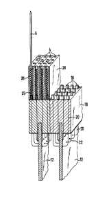
Fig. 1 schematLcally shows an arrangement of and
the manner of supporting individual components which make up
a contaet array 2 having, for example, up to about 256,000
contact positions 4 to be connected through test pins 6 to a
connector carrier or to a printed circuit board 8 under
test. Contacts 4 are arranged in sets of 4 x 32 or 4 x 64,
each to be associated with a contact array plug 10 of the
so-called "bed-of-nails" type which is provided at the top
end of a so-called driver card 12 supporting electronic
components contributing to the electronic testing of the lZ8
(i.e. 4 x 32) contacts 4 to be contacted by each contact
array plug 10. At the bottom end of dr~ver cards 12 there
are provided eontaet plugs (not shown ) to individually
connect driver cards 12 ~contact array modules~, which may
be up to a`oout 2,000 in nu~ber, with electronic control and
test means (not shown) located in the bottom portion of the
test apparatus. Such control and test means need not kR
discussed herein;
As shown in Figs. 1 and 2, eaeh of the contact
array plugs 10 engages or rests on, by opposite narrow edge
end portions thereof, supporting members 14 formed by
vertical plate elements to transmit contaet pressures, whieh
may have eonsiderable magnitude, to frame 16 of the circuit
board testing apparatus. A circuit board 8 to be tested
requires eontaet pressures of abaut 1-2 Uewton per eontaet q
to make reliable contaet, ~iven the a~or~said maximum of
256,00~ contaets, supportlng members 14 together must
~ transmit a total contaet pressure of about 32 tons,
':
. ~ .
_9_

. .
,!`.
,~
.~ ,


' " ' ,', ' ~ . , ' " ` ' ~ ~
' ': ~ ' ' '' . ' ' ' ' ` ` .

Contact array plug 10 consists of an electrically
non-conductive plastic or ceramic material and has on its
top end surface, for example, a total of 4 x 32 = 128 or 4 x
64 = 256 upright contact pins 18 each having a diameter on
the order of 0.8 mm and a height of 2.5 mm. Pins 18 of plug
10 are extended therein by way of co~ductors 20 each
connected to a contact site 22 on printed circuit driver
card 12 to establish electrical connections to electronic
components 24 ~only one shown in Figs. 2a-2b) on driver card
12 which are part of the test circuitry in the circuit board
testing apparatus.
Each one of contact pins 18 extends into a
respective bore 25 in a spring contact array body 26
containing and substantially filled by a respective contact
4 in the form of a compression spring 28 made of an
electrically conductive material. In the preferred
~` embodiment shown in Fig. 3, spring contaet array body 26 is
in the form of a plurality of strips or segments each having
~; a series of bores therethrough lin accordance with the
contact pin arrangement). It is evident, however, that this
element does not have to be a strip-shaped element eontaining
only one row of bores 25. It is within the purview of the
present invention to have any number of rows of bores in a
correspondingly sized spring contact array body 26, as the
size of such bodies depends ultimately on the ease of
fabricatlng them. At present, it is preferred to use bodies
in strip shape haviny therein a single row of four bores as
~t is easier to fabricate them to close toleranees. Such
bodies may be arranged on contact arr~y plug 10 as is shown


--10--

. .
.` ~


.
: ' -' ' ' ,' : ' ' ' ''
' " ' ' ' ' ., ' , ' .

.,
. :

~2~96~

l in Fig. 3. It is also possible to arrange them transversely
thereto (not shown) so that they extend over the width of
each contact array plug 1~. Each hody is about 50 mm in
helght and about 1.27 r~m in width, with the bores therein
having a diameter of about 0.8 r~m and being spaced 1.27 ~m
in a~cordance with the ~onnection site grid.
Spring contact array bodies 26 are plugged on tap
of the contaat plugs lO. Each bore 25, which i5 closed a~
the bottom end by a respectlve contact pin 18, receives a
pressure spring 28 of a special design which f ill5 that bore
completely, i.e. the coils in the resilient portion of the
pressure spring engage the inner walls of the bores so that
maximum dia~eter springs may be ~sed despite the restricted
s~ace condition~.
Ends 30, 31 of springs 28 (shown schematically
orly in Fig. 3) are formed in a particular manner for
directly contacting contact pins 18 of plug 10 or rig~d test
pins 6. As shown in Fig. 4a, spring 28 is coiled at its two
ends (outwardly of its resilient portion 82 having spaced
turns) to have longitudinally contiguous turns the diameters
oi which decrease and then increase in the coilin~ direction
to form an internally tapered portion. Thère thus is
defined at either end of the spring a tapered recess 34 for
receiving the tip of a contact pin 18 or a test pin 6,
respectively. Preferably, springs 28 rnay be wound of spring
steel and may be plated with ~ s~itablc contact material to
~oin the con~iguous turns at the ends of the sprln~.
Fig. 4b shows an alterriative form of a contacting
arrangernent. The sprinq is configured in its top portion as
' .


' , '


' ` .

~2~
.

I described above for engagement of test pin 6, i.e. it has an
internally tapered portion 34 coiled as described above,
whereas its opposite end is coiled to form a pin-shaped
extension 36 the individual turns 33 of which are
contiguous. The aforesaid pin-like extension extends into a
conical xecess in a pin in contact array plug 10 which may
be tapered or cup-shaped. This recess is to be considered
- an alternative to the previously described contact pin 18.
Fig, 4c shows another alternative form of the
I~ compression spring. The end of spring 28 facing the contac~
array plug 10 or the driver card 1~, respectively, is
provided with a contact tongue portion 42 extending
longitudinally of the spring to the associated connection
s1te or contact pad on the surface of driver card 12. As a
re:;ult, the contact array plug 10 has to be provided with
properly positio~ed small-diameter bores 44 through which
onLy the tongues 42 are passed during a~sembly o~ the
contact array. In this case, too, the end of spring 28
fa~-ing test pin 6 i5 coiled to form an internal taper 34 of
2~ lo~gltudinally contiguous spring turns.
It is evl~ent that the particular manner of
contacting longitudinally rigid test pins 6 as provided for
by the inventio~, i.e. through (helical) compression springs~
forming contact elements, can be used advantageously ln
..
2~ circuit board testing apparatus hard-wlred ~or a ~rid of
contacts or connection sites and no~t lncluding a plurality
of identlcal contact array modules for use at any positlon
of the baslc array plate. ~'he present invention is of
partlcular advantage for such latter deslgn concept as it
.' ' ,

-12-
'~' ' , . '

.
:
.~ . .
. . - , - .

~ : '. ' - :
., '. ~ '' ' " '

.
,, ' . " ~ ' .' . ' ' .

~2~391~7~

: l 5eeks, as does the present invention, to greatly reduce the
costs incurred by the contacts required for testing a
circuit board or connection carrier.
. Further, although the present invention has been
described and illustrated with respect to a preferred
embodiment, it will be apparent to those skilled in the art
that various changes and modification~ may be made to the
specifically described and illustrated features without
dppartlng fro~ the scope pf the p-esent lnvention.


.


,
: ` :
~`: . ,
, : : ' . ,.
.
: ~ .


-13-
~: :

,:
: .


.

,'' '

Representative Drawing
A single figure which represents the drawing illustrating the invention.
Administrative Status

For a clearer understanding of the status of the application/patent presented on this page, the site Disclaimer , as well as the definitions for Patent , Administrative Status , Maintenance Fee  and Payment History  should be consulted.

Administrative Status

Title Date
Forecasted Issue Date 1991-09-24
(22) Filed 1987-09-08
(45) Issued 1991-09-24
Expired 2008-09-24

Abandonment History

There is no abandonment history.

Payment History

Fee Type Anniversary Year Due Date Amount Paid Paid Date
Application Fee $0.00 1987-09-08
Registration of a document - section 124 $0.00 1988-09-26
Maintenance Fee - Patent - Old Act 2 1993-09-24 $100.00 1993-08-17
Maintenance Fee - Patent - Old Act 3 1994-09-26 $100.00 1994-08-03
Maintenance Fee - Patent - Old Act 4 1995-09-25 $100.00 1995-07-07
Maintenance Fee - Patent - Old Act 5 1996-09-24 $150.00 1996-08-09
Maintenance Fee - Patent - Old Act 6 1997-09-24 $150.00 1997-07-17
Maintenance Fee - Patent - Old Act 7 1998-09-24 $150.00 1998-08-27
Maintenance Fee - Patent - Old Act 8 1999-09-24 $150.00 1999-06-28
Registration of a document - section 124 $100.00 1999-11-26
Maintenance Fee - Patent - Old Act 9 2000-09-25 $150.00 2000-06-21
Maintenance Fee - Patent - Old Act 10 2001-09-24 $200.00 2001-08-22
Maintenance Fee - Patent - Old Act 11 2002-09-24 $400.00 2003-09-16
Maintenance Fee - Patent - Old Act 12 2003-09-24 $200.00 2003-09-16
Maintenance Fee - Patent - Old Act 13 2004-09-24 $250.00 2004-09-16
Maintenance Fee - Patent - Old Act 14 2005-09-26 $250.00 2005-09-15
Maintenance Fee - Patent - Old Act 15 2006-09-25 $450.00 2006-08-22
Maintenance Fee - Patent - Old Act 16 2007-09-24 $450.00 2007-09-17
Owners on Record

Note: Records showing the ownership history in alphabetical order.

Current Owners on Record
MANIA TECHNOLOGIE AG
Past Owners on Record
DRILLER, HUBERT
MANG, PAUL
MANIA ELECTRONIK AUTOMATISATION ENTWICKLUNG UND GERATEBAU GMBH
Past Owners that do not appear in the "Owners on Record" listing will appear in other documentation within the application.
Documents

To view selected files, please enter reCAPTCHA code :


To view images, click a link in the Document Description column. To download the documents, select one or more checkboxes in the first column and then click the "Download Selected in PDF format (Zip Archive)" or the "Download Selected as Single PDF" button.

List of published and non-published patent-specific documents on the CPD .

If you have any difficulty accessing content, you can call the Client Service Centre at 1-866-997-1936 or send them an e-mail at CIPO Client Service Centre.


Document
Description 
Date
(yyyy-mm-dd) 
Number of pages   Size of Image (KB) 
Representative Drawing 2002-04-03 1 11
Description 1993-10-22 13 508
Drawings 1993-10-22 4 146
Claims 1993-10-22 16 551
Abstract 1993-10-22 1 28
Cover Page 1993-10-22 1 23
Fees 2003-09-16 1 47
Fees 1999-06-28 1 39
Fees 1997-07-17 1 41
Fees 2004-09-16 1 37
Fees 2000-06-21 1 41
Fees 1998-08-27 1 45
Fees 2001-08-22 1 38
Fees 2005-09-15 1 34
Fees 2006-08-22 1 45
Fees 2007-09-17 1 51
Fees 1996-08-09 1 40
Fees 1995-07-07 1 41
Fees 1994-08-03 1 36
Fees 1993-08-17 1 31