Note: Descriptions are shown in the official language in which they were submitted.
HOUSING STRUCTURE FOR PAGIN~ RECEIV}iR
13ACXGROUND OF THE INVENTION
The pr2sent invention relates to the structure of a housing of
a paging receiver and, more particularly, to the housing
structure of a pa~ing receiver of the type having a storage
5 device and an exclusive write terminal for writing code in the
storage de~ice.
There is an increasin~ demand for a paging receiver which is
miniature, inexpensive, reliable and easy to maintaill.
Especially, in the aspect of structure, the demand for easy
10 maintenance and high reliability is keen. A prior art paging
receiver usually inc'udes a chamber for accommodating a printed
circuit board on which an electrically erasable programmable
read only memory (EEPRl:)M) or like storage device for storing a
pagin~ number is loaded. Another chamber adjoiIls the above-
15 mentioned chamber to receive a battery therein. The EEPROM onthe printed circuit board is connected by leads to a write
terminal for writing the paging number in the EEPROM. The
write terminal is provided on the priIIted circuit board or fitted
to a part of a housing of the r0ceiYer to show itself for easy
20 access from the outside.
lx~
-
A drawback with the arrangement wherein the write terminal
is mounted on the printed circuit board is that the code cannot
be written in the EEPROM without disassembling the housing in
which the printed circuit board is accommodated and thsn
5 connecting a writing apparatus to the write termin~l. This not
only needs troublesome operations but also contradicts to the
demand for easy maintenance. On the other hand, the write
terminal fitted to a part of the housing brin8s about a problem
that static electricity is apt to be conducted to the EEPROM and
10 various integrated circuits Yia the write terminal. Such static
electricity would destroy the code stored in the EEPROM, cause
the receiver to malfunction, and even destroy the whole circuitry
in the receiver, critically lowering the reliability of the receiver.
SUMMARY OF THE INVENTION
It is therefore an obiect of the present invention to provide a
housing structure for a paging receiver which facilitates
maintenance, promotes easy writing of code, and has high
reliability of operation.
~0 It is another object of the present invention to provide a
generally improved housing structure for a paging receiver
A structure of a housin~ for a paging receiver of the present
invention comprises a chamber for accommodating a printed
circuit board on which at least a storage device for storing code
25 and a write terminal for writing the code in the storage device
are mounted, a battery case provided in a space which adjoins
the chamber and having an opening which is exposed to the
outside, and a window formed throuth a part of the battery case
which adjoins the chamber and communicated to the chamber.
The write terminal being located on the printed circuit board to
face the window such that the write terminal is connectible to a
connector of a writing apparatus which is inserted throuzh the
window as needed.
BRIEF DESCRIPTION GF THE D~AWIN&S
The above and other objects, feat~res and advantages of the
present invention will become more apparent from the following
detailed description taken with the accompanying drawings in
which:
Figs. 1 and 2 are perspective views each showing a different
prior art housing structure for a paging receiver;
Fig. 3 is a perspective view showing a housing structure
embodying the present invention;
Fig. 4 is a fragmentary section along line IV-IY of Fig. 3;
2 0 Fig. 5 is a perspective view demonstrating how to write a
paging number with the embodiment of Fig. 3;
Fig. 6 is a fragmentary section associated with Fig. 5;
Fig. 7 is a perSpectiYe Yiew showing another embodiment of
the present invention; and
Fig. g is a fragmentary section associated with Fig. 7.
0~3
DESCRIPTION OF THE PREFERRED EMBODIMENTS
To better understand the present inYention, a brief reference
will be made to prior art housing structures for a paging
receiver which are shown in Figs. 1 and 2.
Referrin~ to Fig. 1, a prior art housing 10 for a paging
receiver accommodates therein an EEPROM or similar storage
device 12 for storing desired code which is assigned: to t~e
paBing receiver. A battery case 14 for receiving a batterY
therein is built in the housing 10 so that a chamber 16 is defined
by the battery case 14 and the housing 1 û. A printed circuit
board 18 is disposed in the chamber 16. The battery case 14
has an opening 2 0 which is usually closed by a lid 2 2 which
forms a part of the housing 10. The EEPROM 12 is mounted on
the printed circuit board 18 and connected bY leads 26 and 28 to
a write terminal 2 4 so that the code may be written in the
EEPROM 12 via the terminal 24. While the write terminal 24
shown in Fig. 1 is directly mounted on the printed circuit board
18, it may be mounted in a part 10a of the housin~ 10 as shown
in Fig. 2.
Each of the prior art housing structurQs shown and describsd
has a problem left unsolved, as previously stated. Specifically,
with the arrangement of Fig. 1, it is necessary to write co~e in
the EEPROM 12 by disassembling the housing 10 in which the
printed circuit board 18 is accommodated and then connecting a
25 writing apparatus ~not shown) to the write terminal 24. This is
12~?0~3
not only troublesome but also obiectionable from the easy
maintenance standpoint. On the other hand, the structure of
Fig. 2 suffers from a drawback tbat static electricitY is apt to be
conducted to the EEPROM 12 and various integrated circuits Yia
5 the write terminal 24 which is exposed to the outside through the
housing 1 Oa. Such static electricitY would distroy the data
stored in the EE:PROM 12, cause the receiver to malfunction, and
evsn destroy the whole circuitry stored in the receiver, critically
lowering the reliability of the receiver.
Referring to Figs. 3 to B, there are shown preferred
embodiments of the present invention which are free from the
dra~backs particular to the prior art housing structures as
discussed abo~e. In Figs. 3 to 8, the same or similar structural
elements as those shown in Figs. 1 and 2 are designated by like
reference numerals.
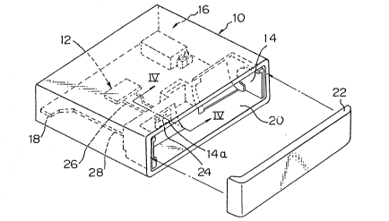
In Figs. 3 and 4, a housing 10 in accordance with the
present invention is generally configured in a rectangular
~arallelepiped. A battery case 14 is built in the housing 10
ad jacent to an opening 2 O of the housing 10 and defines a
2 O chamber 16 in cooperation with the housing 10 . A lid 2 2 is
removably mounted on the housin~ 10 to clo~e the opening 2 O
while forming a part of the housing 10, whereby a chamber for
receiving a battery ~not shown) is defined. The housing 10,
battery case 14 and lid 22 are each made of a non-conductive
25 material such as polycarbonate. A printed circuit board 18 is
0~3
disposed in the chamber 16 while an EEPROM 12 is mounted on
the circuit board 18 together with various kinds of circuit parts.
A write terminal is loaded in one end portion of the printed
circuit board 18 and electrically connected to the EEPROM 12 by
leads 26 and 28. That part of the battery case 14 which faces
the write terminal 24 is provided with an opening or window
14a. This window 14a allows a connector 32 of a: writing
apparatus 3 0 which will be described later with reference to
Figs. 5 and 6 to be inserted through the window 14a into
electrical connection with the write terminal 24.
Figs. 5 and 6 show how a desired code is written in the
EEPROM 12. Specifically, the lid 2 2 (Fig. 3 ) is removed to
expose the battery case 14 to the outside, and then the
connector 32 connected to the writing apparatus 30 by a wiring
34 is inserted into the housing 10 Yia the window 14a to be
connected to the write terminal 24. In this condition, a code
may be written in the EEPROM 12 which is connected to the
writin~ apparatus 30 via the write terminal 24 and leads 26 and
28. In Fig. 6, the reference numeral 36 designates a resilient
contact for connection.
In this particular embodiment, although the write terminal
24 is ent*ely accommodated in the housing 10, a code can be
written in the EEPROM l 2 merelY by remoYing the lid 2 2 and
inserting the connector 32 through the svindow 14a of the battery
25 case 14 into connection with the write terminal 24. This
.3
facilitates ~riting operation and promotes easy maintenance.
As shown in Fig. 4, assume that the distance between the
write terminal 24 and the inner surface o~ the battery case 14 is
~, the thickness of the battery case 14 is b, the inside dimension
5 of the battery case 14 is c, and the thickness of the lid 22 is d.
Then, the write terminal 24 which is not exposed to the outside
is spaced apart from the outer surface of the battery case 14 by
a distance a + b and, when the lid 22 is attached to the housing
10, it is spaced apart from the outer surface of the lid 22 by a
10 distance a + b + c + d. The influence of static electricity
developed outside the housing 10 on the interior of the housing
10 is reduced in proportion to the distance e + ~ or
+ b + c ~ d to protect the EEPROM 12 and other various
circuit parts from destruction. Such a structure, therefore,
15 enhances reliable operations of the pagirlg receiver.
Referring to Figs. 7 and 8, another embodiment of the
present inventlon is shown. This embodiment is essentiallY
similar to the previous embodiment except that a non-conductive
label 38 is adhered to the battery case 14 to close the window
2 0 1 4a, the label 3 8 showing the code which is stored in the
EEPROM 12. This alternative embodiment has an advant~ge that
a person can see the label 38 and therefore the content stored in
the EEPROM 12 simply by removing the lid 22, not to speak of
the various advantages described in relation to the first
25 embodiment. In addition, the label 38 which closes the window
~3
, ,,
--8--
14a further enhances the resistivity of the EEPROM 12 and others
to static electricity and pre~ents dust, water and other
impurities from reaching the write ~erminal 24 aDd printed circuit
board 18 through the window 14a.
In summary, a housing for a paging receiver in accordance
with the present invention includes a battery case which forms a
part of the housing and communicates with the interiot of the
housing through a window. A connector of a writing apparatus
may be inserted into the housing through the window into
connection with a write terminal which is electrically connected to
a storage device. Hence, a code can be written in the storage
device simply by removing a lid which is adapted to close the
battery case. This promotes easy writing operation as well as
easy maintenance. Since the write terminal is not exposed to the
outside of the housing, resistivity to static electricity and
hermetic sealing against impurities are enhanced to offer
unprecedented reliability of operation.
Various modifications will become possible for those skilled
in the art after receiving the teachings of the present disclosure
without departing from the scope thereof.