Note: Descriptions are shown in the official language in which they were submitted.
07~
62901-7
Back~round of the Invention
1. Field of the Invention
This invention relates generally to electrical
jackfields and is concerned more partlcularly with an electrical
jackfi~ld having a linear array of juxtaposed jack modules and
respective aligned printed circuit boards which are rontally
removable from the jack~ield.
2. Discussion of the Prior Art
A jackfield assembly may comprise a housing having
therein a linear array of electrical jack modules which are
disposed in side-by-side relationship along a front portion of the
housing to have respective plug-receiving end portions extend
through a front panel of the housing. In U.S. patent ~o.
4,770,639 which issued on September 13, 1988, there is disclosed a
channelized jackfield having a housing wherein a plurality of
substantially planar channels extend in juxtaposed relationship
from a front portion to an opposing rear portion of the housing.
Each of the channels has inserted therein, through a front opening
of the housing, a respective tri-jack module with a slab-like body
having a narrow side uppermost in ths housing. Also, each of the
channels has inserted therein, through a rear opening of the
housing, a respective printed circuit board which is dispo~ed on
edge within the housing.
~J9 ~
Each of the tri-jack modules has a plug-receiving end
portion comprising a vertically extending front plate having
protruding therefrom a vertical series of three mutuall~
spaced sleeves which extend through a front panel covering
the front opening of the housing. In each o~ the modules
there is a stacked array of three electrical jacks, each of
which is aligned with a respective sleeve extending through
the front plate o~ the module. Each of the electrical jacks
comprises a plurality of electrical switches having respective
moveable leaf spring members electrically engageable with
respective stationary members. Also, the moveable members of
an e~ectrical jack are disposed for actuation by a patch cord
end plug inserted through the aligned sleeve. The end plug
has mutually insulated portions shaped for electrically con-
tacting respective moveable members of the electrical jack~
The moveable members and the stationary members of the
electrical switches comprising the three electrical jacks
stacked in each module are attached to respective terminals
which extend in a linear array from a rear portion of the
module adjacent the aligned printed circuit board. The
terminals in the linear array extend into electrical engage-
ment with respective contacts of a connector secured to the
adjacent end portion of the printed circuit board. Contacts
of the connector are electrically connected through respective
conductors of the printed circuit board to respective terminal
o~
~ 2901-738
lugs which extend from an opposing end portion of the printed
circuit board. The terminal lugs project out of the rear openiny
of the housing for electrical connection, a~ by wire-wrapping, for
example, to respective conductors of an umbilical wire harness.
In U.S. patent No. 4,772,562 which issued on September
20, 1988, there i6 disclosed a channelized jackfield similar to
the described jackfield but having a split front panel. The split
front panel provides means for inserting or removing an individual
jack module and the aligned printed circuit board as a unitary
subassembly from the front of the housing without diæturbing the
patch cord connections between the other modules of the linear
array. However, this embodiment has the drawback that all of the
terminal lugs extending from the printed circuit boards project
ou~ of the rear of the housing. The housing may be mounted in a
tier of racks which extends linearly over a considerable distance,
such as thirty feet, for example. As a result, if a testing
technician wishes to connect a wire to or disconnect a wire from a
terminal lug when inserting a patch cord end plug in~o a sleeve of
a jack module, the terminal lugs are not readily accessible from
the front of the jackfield assembly. Consequently, the testing
operation usually requires two technicians, one technician at the
rear of the rack for connecting or disconnecting the wires and the
other technician at the front
lZgO~
of the rack for inserting the patcn cord end plug or with-
drawing it from the sleeve of a jack module.
-- 4 --
` ~9~7S
Summary of the Invention
These and other disadvantages of the prior art are
overcome by this invention providing a channelized jackfield
with a housing having a front opening including a lower
portion filled with a linear array of juxtaposed vertical
legs of respective dielectric L-shaped brackets. The vertical
legs extend integrally downward from adjacent end portions of
respective orthogonal legs of the brackets which project
forwardly of the housing in juxtaposed relationhip with one
another. Also, each of the vertical legs has a width defining
the width of an aligned planar channel extending into the
housing t3 a rear wall thereof.
The vertical legs of the L-shaped brackets are secured
to adjacent end portions of respective printed circuit ~oards
slidably disposed on edge in the respectively aligned channels~
Each of the vertical legs of the dielectric brackets has
disposed therein a vertical series of mutually spaced slots
through which respective terminal lugs extend outwardly from
the front of the housing. The terminal lugs are connected
electriclly through respective conductors of the printed
circuit board to respective contacts of a connector secured
to an adjacent end portion of the board above the vertical
leg of the L-shaped ~racket.
Each of the forwardly projecting, orthogonal legs of the
brackets has an upper surface provided with a collinear groove
1~9~7~i
62901-738
wherein a side rail portion of a respective tri-jack module is
slidably di~posed. The tri-jack module has protruding from an
inner end portion thereof a linear series of mutually spaced
terminals which extend into electrical engagemen~ with respective
contacts of the connector secured to the adjacent end portion of
the printed circuit. Thus, some of the module terminals are
connected through the engaged contacts of the connector and
eonnecting conductors of ~he printed circuit board to respective
terminal lugs extending outwardly from the front of the housing
below the module. Accordingly, these ter~inal lug~ are readily
accessible to a testing technician lnserting patch cord end plugs
into jack sleeves o~ the module.
The invention may be summarized, according to a firs~
aspect, as a printed circuit board assembly comprising: a prin~ed
circuit board having an edge with a right angle connector adapted
for receiving and removably mating with an electrical jac~ module,
said printing clrcuit board having a plurality of printed circuit
conductors with respective end portions disposed in spaced
relationship with one another at a portion of said edge adjacent
~o said right angle connector; a linear array of laterally spaced
terminals disposed along said portion of said edge, each of said
terminals having a proximal end portion connected electrically to
a respective one of said end portions of said conductors and
having a distal end por~ion projected outwardly of said edge of
said board; and a dielectrical bracket having a first leg disposed
along said portion of said edge and being secured to sald board,
said bracket having an orthogonal second leg integrally joined to
~0~75
62901-738
an end portion of said first leg and projected out~tardly of said
edge of said board, said first leg of said bracket having disposed
therein a linear array of mutually spaced apertures through which
respective distal end portions of said terminals extend, said
orthogonal second leg of said bracket having a collinear surface
provided with a channel adapted for receiving said electrical jacX
module in slidiny engagement.
Accordiny to a second aspect, the present invention
provides An electrical jackfield comprising, a housing having a
front opening extended laterally between a vertical pair of
opposin~ side walls of the housing, said front opening having an
upper porkion and a lower portion; a linear array of juxtaposed
jack modules having respective slab-like bodies slidably disposed
in said upper portion of said front openiny, each of said slab-
like bodies having a narrow side uppermost and having a front end
provicled with a forwardly protruding, vertical series of plug-
receivlng sleeves; a linear array of dielectric brackets having
respective vertical legs slidably supported in side-by-side
relationship with one another in said lower portion of said front
opening, each of said vertical legs having protruding forwardly
therefrom a vertical series of mutually spaced terminals wherein
each of said vertical legs is disposed in registration with a
respective one of said modules in said upper portion of said front
opening; said housing including upper faceplate means for closiny
said upper portion of said front opening; and said linear array of
dielectric brackets comprising a lower faceplate means for closing
sai~ lower por~ion of said front opening wherein said lower
6a
'J3~9~o~
62901-73~
faceplate means i~ recessed with respect to said upper faceplate
means said dielectric brackets include respective orthogonal legs
extended integrally forward from upper end portions of said
vertical legs o~ said dielectric brackets wherein each of said
orthogonal legs has an upper surface provided with a collinear
channel means for slidably receiving therein a lower side portion
of the respective module disposed in reyistration with said
vertical leg of the respective dielectric bracket.
According to a third aspect, the presen~ lnvention
provides an electrical jackfield comprising5 a housing having a
rear portion and having an opposing front portion with a front
opening extended laterally between a vertical pair of opposing
side walls of said housing, said fron~ opening having an upper
portion and a lower portions; a linear array of laterally spaced
printed circuit boards extended from said rear portion to said
front portion of said housing, each of said printed circuit boards
being slidably insertable on a longitudinal edge thereof into said
housing through said front opening and having a plurality of
conductors with first end portions spaced apart in an upper front
end portion of said board aliyned with said upper portion of said
front opening, said conductors having respective second end
portions spaced apart in a lower forward end portion adjacent a
forward edge portion thereof aligned with said lower portion of
said front opening; a linear array of juxtaposed jack modules
having respective slab-like bodies slidably disposed with
respectiYe narrow sides uppermost in said upper portion of said
front opening, each of said slab-like bodies belng aligned with a
6~
` 1~9~,~375
~ 2901-73g
respective one of said printed circuit boards and having a rear
end from which a vertical series of terminals extends into
electrical connecking relationship wi~h a respective one of said
first end portions of said conductors; and a linear array of
dielectric brackets having respective vertical legs slidably
supported in side-by-side relationship with one another in said
lower por~ion of said front opening, each said vertical legs being
secured to said lower forward end por~ion of a respective one of
said boards and having projected forwardly therefrom a vertical
series of mutually spaced ~erminal lugs wi~h proximal end portions
connected electrically with a respective one of said second end
portions o~ said conductors.
6c
Brief Description of the Drawings
For a better understanding of the disclosed invention,
reference is made in the following detailed description to the
accompanying drawings wherein:
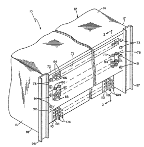
FIG. 1 is an isometric view of the jackfield assembly
embodying the invention;
FIG. 2 is a cross-sectional view taken along the line 2-2
shown in FIG. 1 and looking in the direction of the arrows;
FIG. 3 is an isometric view of the L-shaped bracket
shown in FIG. 2;
FIG. 4 is an isometric view of the bracket shown in FIG.
3 and secured to the printed circui~ board shown in FIG. 2; and
FIG. 5 is a cross-sectional view taken along the line 5- 5
shown in FIG. 4.
lS
~9~
629~1-738
Description of the Pre~erred Embodiment
Referring to the drawings wherein like characters of
reference designate like parts, there is shown in FIGS. 1 and 2 a
channelized jackfield assembly 10 comprising a sheet metal housing
12 made of electrically conductive material, such as anodized
aluminum, for example. Housing 12 includes a top wall 14
integrall~ joined to re~pective opposlny side walls 16 and 17
which are flxedly attached, as by welding, for example, to a
bottom wall 18 of the housing. Within housing 12, there is
attached, as by rivets, for example, to the top wall 14 and the
bottom wall 18 respective plank-like, wafer guides 20 and 22 which
extend laterally from adjacen~ ~he side wall 16 to adjacent the
opposing side wall 17 of housing 12. Wafer guides 20 and 22 are
made of dielectric material, such as molded plastic material, for
example, and are fully disclosed ln the aforementioned U.S. patent
No. 4,772,562.
The wafer guides 20 and 22 are disposed in aligned
opposing relationship with one another and have facing surfaces
provided with respective linear series of laterally spaced grooves
or channels 24 which extend forwardly and rearwardly of the
housing 12 in substantially parallel relationship with one
another. Corresponding channels 2~ in the respective wafer guides
20 and 22 are dlsposed in registration with one
~9~
another for slidably receiving therein opposing side edge
portions of respective printed circuit boards 26 whic'n are
inserted from the front of housing 12. The printed circuit
boards 26 have respective rear end portions 27 which abut a
dielectric rear wall portion 28 supported along an elongated
opening 30 in a metallic rear wall 31 of housing 12. Extend-
ing rearwardly from the rear end portion 27 of printed circuit
boards 26 are respective vertical arrays of mutually spaced
terminal lugs 32 made of rigid electrically conductive
material, such as tin plated brass, for example. Each of the
terminal lugs 32 has a proximal end portion electricall~
connected, as by soldering, for example, to an aligned pair
of eyelets 34 in the adjacent rear end portion 27 for electrical
connection to a respective connecting conductor 36 of the
supporting board 26. Also, each of the terminal lugs 32 has
a distal end portion passed through an aligned aperture 38 in
the dielectric rear wall portion 28 of housing 12 for
electrical connection, as by wire-wrapping, for example, to a
respective external conductor (not shown)
The printed circuit boards 26 have lower side portions
including rear shoulder portions 40 which abut a vertical
partition 42 of housing 12. Partition 42 has an upper end
portion integrally joined to an orthogonal, rearwardly ex-
tending partition 44 of housing 12. The respective partitions
42 and 44 extend laterally from ad~acent the side wall 16 to
1i~9~75
62901-738
adjacent the opposing side wall 17 of housing 12. Vertical
partition 42 has a lower marginal portion a~tached, as by welding,
for example, to an adjacent edge por~ion of botto~ wall 18. The
rearwardly extending partition 44 has a rear edge portion
~imilarly a~tached to a portion of rear wall 31 adjacent the lower
edge of opening 30. Supported on inner surface portions of the
respective partitionæ 42 and 44 ad~acent the integral juncture
thereof is a right angle, buss housing 46 which extends laterally
from adjacent side wall 16 to adjacent the opposing side wall 17
of housing 12. Structural details of the buss houæing 46 are more
fully dlsalosed ln the aforementioned U.S. patent No. 4,772,562.
Buss housing 46 includes a connector portion 48 which
extends along the vertical partition 42 of housing 12 and a plank-
like portion 50 which is at~ached, as by rive~s 51, for example,
to the rearwardly extending partition 44 of housing 12. The
plank-like portion 50 is similar ~o the wafer guides 20 and 22,
respectively, and has disposed in its upper surface a linear array
of laterally spaced channels 52 which extend forwardly and
rearwardly of housing 12. Each of the channels 52 is aligned with
a respective pair of opposing channels 24 ln the respective wafer
guldes 20 and 2Z for slidably receiving an aligned edge portion of
the inserted printed circuit board 26. Also, each of ~he prin~ed
circuit boards 26 has lnserted in~o the right-angled connector
~L~9(~(~75
62901-73~
portion 48 of buss housing 46 an aligned portion whereon
respective buss conductors 54, 56 and 58 have terminal end
portions disposed in vertically spaced relationship with one
another. As a result, the printed circuit boards 26 have their
respective buss conductors 54 connected electrically to a negative
for~y-eight volt source, their respective buss conductors 56
connected to system ground and their respective buss conductors 58
co~nected to signal ground.
The buss conductors 54 of the respective boards 26 are
routed to forward neck end portions 60 of the printed circuit
boards which have secured thereto respective forwardly extending,
lamp jack housings 62 made of dielectric material. Structural
details of the lamp jack housings 62 are more fully disclosed in
the aforemen~ioned U.S. patent No. 4,772,562. The lamp jack
housings 62 have forward end portions terminatiny in respective
block-like rims 64 which define openings of respective sockets
(not shown) wherein respective lamps 66 are installed. Each of
the lamps 66 has a pair of laterally spaced terminal conductors
(not shown) inserted into electrical engagement with respective
aligned contacts (not shown) in the receiving housing 62 for
electrical connection of respective pairs of aligned eyelets 67
and 68 in the neck end portions 60 of the supporting board 26.
The pairs of aliyned eyelets 67 in the respectlve boards 26 are
1?~9~ 7~;
62901-738
connected electrically to the respective buss conductor3 54
thereof; and the pair of aligned eyelets 68 are connected
electrically to respective conductors 70 of the printed circuit
boards 26. The respective block-like rims 64, as sho~1n more
clearly in FIG. 1, extend in juxtaposed relationship with one
another through an elongated rectangular opening 71 in an upper
front panel 72 of the jackfield assembly 10. Upper front panel 72
is secured to the housing 12 by readily removable fastening means,
such as screws 73, for example.
Each of the lamp jack housings 62 has a lower side
surface wherein a collinear channel 74 is disposed for slidably
recelving an aligned pair of rails 76 which project upwardly from
a slab-like body of a tri-jack module 78 having a narrow side
uppermost. Each of the tri-jack modules 78 has extending
rearwardly from an inner end of its slab-like body a vertical
array of mutually spaced terminals 80. The terminals 80 of each
module 78 are slldably inserted into electrical engagement with
respective contacts (not shown) in a dielectric body of an aligned
connector 82. Structural details of the tri-jack modules 78 and
the respective aligned connectors 82 are more fully disclosed in
the aforementioned U.S. patents 4,770,639 and 4,772,5S2.
Each of the modules 78 has a forward end portion
terminating
0~3~5
in a forwardly projec~ed landing 84 which extends laterall~
between three vertically spaced sleeves 86, ~7 and 88,
respectively. The sleeves 86, 87 and 88 extend forwardly of
the respective landings 84 from within the slab-like bodies
of the respective modules 78. Landings 84 of the respective
modules, as shown in FIG. 1, extend in juxtaposed relationship
with one another between respective opposing edge portions of
the upper front panel 72 and an intermediate front panel 90.
The three vertically spaced sleeves 86, 87 and 88 of each
module 78 are disposed between opposing semi-circular notches
(not shown) in respective aligned edge portions of the upper
front panel 72 and the intermediate front panel 90. Front
panel 90 is secured to the housing 12 by readily removable
. fastening means, such as screws 91, which are similar to the
screws 73, for example. Thus, the upper front panel 72 and
the intermediate front panel 90 constitute a split front
panel means which is readily removable for permitting tri-
jack modules 78 to be removed from or inserted into electrical
engagement with an aligned connector 82 from the front of
housing 12.
Within the slab-like bodies of the respective modules
78, the sleeves 86, 87 and 88 are aligned with respective
electrical jacks (not shown), each of which comprises a
stacked plurality of moveable switch members engageable
electrically with respective stationary switch members (not
- 13 -
~2~ 75
shown). The moveable switch members of each electrical j~ck
(not shown) are actuated by a conventional jack plug (not
shown) inserted through the aligned sleeve from the fron~ of
jackfield assembly 10. Also, the moveable switch members
(not shown) and the stationary switch members (not shown~ in
the slab-like body of each module 78 are connected electrically
to respective terminals 80 extending rearwardly thereof. The
terminals 80 of each module 78 are connected electrically
through respective contacts of the aligned connector 82 to
respective eyelets 92 disposed in adjacent central portion of
the supporting board 26. Some of the eyelets 92 are connected
electrically to respective printed circuit conductors 36
which are connected electrically through respective eyelets
34 to respective terminal lugs 32 extending rearwardly out of
housing 12. Thus, the respective modules 78 have some of
their switch members, such as the moveable switch members
(not shown), for example, connected electrically to the
terminal lugs 32 extending out of the rear of jackfield
assembly 10.
As shown in FIG. 1, there is attached to opposing side
walls 16 and 17 of housing 12 respective mounting brackets 96
and 97 which are intended for installing the jackfield assembly
10 in a tier of racks (not shown) which may extend linearly
for a considerable distance. Consequently, the terminal lugs
32 protruding from the rear of jackfield assembly 10 may not be
- 14
7~
readily accessible to a testing technician inserting test
jack plugs into the sleeves 86, 87 and 88 protruding from the
front of jackfield assembly 10. Therefore, it would be
desirable to have some or all of the terminal lugs of the
respective boards 26 accessible at the front of the jackfield
assembly 10 for any changes in connecting wiring that may be
required during testing. However, it also would be desirable
to have the capability of removing through the front of
jackfield assembly 10 anyone of the channel defining sub-
assemblies comprising a respective printed circuit board 26
having secured thereto a respective lamp jack housing 62 and
a respective module 78 if still installed.
Accordingly, these and other problems are solved by this
inventive embodiment having at least some of the eyelets 92,
such as those connected to respective stationary switch
members (not shown) of the aligned modules 78, for example,
connected electrically to respective printed circuit conductors
g8 which are routed to lower forward end portions 100 of the
respective boards 26. In the lower forward end portions 100,
the conductors 98 are electrically connected to respective
forwardly extending pairs of aligned eyelets 102 which are
disposed adjacent lower forward edges of the respective
boards 26. The pairs of eyelets 102 of each printed circuit
board 26 are laterally spaced apart and have attached thereto
proximal end portions of respective terminal lugs 104 which
- 15 -
have opposing distal end portions extended forT,Jardly of th~
adjacent forward edge of the respective board 26. Thus, the
printed circuit boards 26 are disposed vertically in housing
12 have extended from respective lower forward end portions
thereof respective vertical arrays of laterally spaced terminal
lugs 104.
As shown in FIG. 3, each of the boards 26 has the proximal
end portions of its respective terminal lugs 104 disposed
between a covered surface of its lower forward end portion
100 and a covering plate-like portion 106 of a respective
L-shaped bracket 1080 Each of the brackets 108 is made of
dielectric material, such as molded plastic material, for
example, and has protruding integrally from the surface oF
its plate-like portion 106 adjacent the respective board 26 a
pair of mutually spaced pins 109. The pins 109 are press-
fitted into respectively aligned holes (not shown) which
extend through the thickness of the respective board 26.
Also, each of the vertical plate-like portions 106 has
extended integrally from its upper and lower edges and beyond
the thickness of the respective board 26 mutually aligned,
flexible fingers 111 and 112, respectively. The fingers 111
and 112 have distal end portions provided with ramp-like
sloped surfaces terminating in respective abrupt shoulders
which lockingly engage the exposed surface of the lcwer
forward end portion 100 of -the respective board 2~. Moreover,
- 16 -
~?~9~ 75
each of the plate-like portions 106 has a forward edge from
which an integral vertical wall 110 extends be~ond the thick-
ness of the respective board 26 and has disposed therein a
vertical array of transverse slots 118 which are open-ended~
The slots 118 extend from the distal edge of wall 110 and are
spaced apart by interposed flexible fingers 113, 114, 115 and
116, respectively. The fingers 113 and 116, as shown in
FIG. 5, have distal end portions provided with respective
right-angle shoulders llg which lockingly engage the exposed
surface of the lower forward end portion 100 of the respective
board 26.
Thus, when the pins 109 extending from the plate-like
portion 10~ of each bracket 108 are press-fitted into the
. respective aligned holes in the lower forward end portion 100
of the respective board 26, the edges of the portion 100
cause the respective fingers 111, 112, 113 and 116 to flex
backward and return for locking engagement with the exposed
surface of the lower forward end portion 100. Simultaneously,
the terminal lugs 104 extending forwardly of the lower forward
end portion 100 are inserted laterally into respectively
aligned slots 118 in the vertical wall llO of the respective
bracket 108. Consequently, as shown in FIG. l, the vertical
walls 110 of the respective brackets 108 are disposed in
juxtaposed relationship with one another to constitute a
lower portion of the front faceplate of jackfield assembly lO.
1?~9~3~7~
.
As shown in FIGS. 3 and 4, the vertical wall 110 of each
bracket 108 has an upper end portion integrally joined to a
forwardly extending leg 120 which comprises an orthogonal
extension of the respective vertical wall 110. Each of the
legs 120 has an upper surface provided with an integral
plateau portion wherein a collinear channel 122 is disposed
for slidably receiving a pair of aligned rails 77 projecting
downwardly from a lower side surface of a respective coplanar
module 78. Also, each of the legs 120 has depending integrally
from its lower surface a collinear rib 124 which has an énd
portion integrally joined to the respective forward wall 110.
Distal end portions of the legs 120 and the depending ribs 124
are integrally joined to forward end caps 126 of the respective
brackets 108.
As shown more clearly in FIG~ 2, there is disposed against
the juxtaposed end caps 126 of the respective brackets 108 a
forward portion of a right-angled support plate 130 which a
lower portion disposed beneath the ribs 124 of the respective
brackets 108. The support plate 130 is secured to the housing
12 by readily removable fastening means, such as screws 132,
for example. Thus, when the respective front panels 72 and
90 are removed from housing 12 and the support plate 130 is
removed therefrom any one of the channel-defining subassemblies
comprised of a respective printed circuit board 26, the
attached lamp jack housing 62 and the aligned module 78 may
- 18 -
?,~7~
be slidably removed through the front of jackfield assembl~
10 .
Thus, there has been disclosed herein a jackfield assembly
having a housing provided with front faceplate comprised of an
upper portion wherein there is disposed a linear array of
juxtaposed electrical jack modules and comprised of a lower
portion wherein there is disposed a linear array of juxtaposed
L-shaped brackets having vertical legs from which protrude
respective vertical arrays of mutually spaced terminals.
Each of the vertical arrays o mutually spaced terminals i5
disposed in registration with a respective module having
protruding therefrom a vertical series of plug-receiving
sleeves with aligned switch members electrically connected to
respective terminals of the vertical array. Accordingly, the
terminals of the vertical arrays are readily accessible to a
test technician inserting jack plugs into the sleeves of the
modules.
From the foregoing, it will be apparent that all of the
objectives have been achieved by the structures and methods
described herein. It also will be apparen~, however, that
various changes may be made by those skilled in the art
without departing from the spirit of the inventive subject
matter, as expressed in the appended claims. It is to be
understood, therefore, that all matter shown and described is
to be interpreted as illustrative and not in a limiting sense.
- 19 -