Note: Descriptions are shown in the official language in which they were submitted.
` ~Z~(~081
Background of the Invention
This invention relates to improvements in multicarrier
demodulators of a type which are particularly useful in
telecommunication systems employing satellite transmissions.
Multicarrier demodulators intended for use in satellite
communication systems of the kind shown in Fig. 1 are well
known. Referring to Fig. 1, various vehicles including
aircraft 10, ships 11 and trucks 12 are interconnected with
each other for radio communication via a satellite 13 and
ground station 15. The satellite 13 receives uplink signals
from one or more of the vehicles in the L band of frequen-
cies, using a frequency division multiplexing mode (FDM),
that includes up to 800 different channels. The satellite
retransmits such data signals to the ground station 15 over
the C band of freqllencies using a time division multiplex
(TDM) mode of transmission. From the ground station 15, the
data is retransmitted to other ones of the mobile vehicles or
stationary receivers.
The multicarrier demodulator of the present invention is
employed as part of the transponder system aboard the
satellite, as shown in block diagram form in Fig. 2. Refer-
ring to Fig. 2, the FDM uplink signal is received by the
satellite antenna 18, is converted to a signal SFDM and
passes to a first carrier frequency converter 19 having a
-- 2 --
,' ~
xeference signal generator l9a connected thereto. The
converted signal SIF is passed through a filtering circuit 20
to a sampling circuit 21 and then to an analog-to-digital
converter circuit 22, where the signal is digitalized as
known in the art. After being digitalized, the signal is
then passed to a frequency division demultiplexer 23, also
known in the art, whexe the signal is separated into the
digitalized signals for each of the many different channels 1
to L, inclusive. The digital separated signals for each
channel are then demodulated by demodulator circuits 24a, 24b
. . . 2~n for each channel. In the satellite transponder,
all of the different data signals from the different channels
are combined by a multiplexer 25 and processor 27 into a time
division multiplexer mode, modulated at 28 and transmitted in
the different multiplex mode and at the different frequency
band, by the satellite transmitting antenna 29.
The requirements for the processing and demodulating of
the different signals for the channels 1-L are as follows. A
high sampling rate f fsI = 4LB at sampling circuit 21 is
re~uired in relation to the number of channels L and the
bandwidth B. This is reduced to a sampling frequency of
fso = 2B for the individual output signals for the plural L
channels. The desired signal spectrum at the output of the
demultiplexer 23 should be present in a centered position
- 3 -
~91:3Q83~
27371-18~
around a center band frequency fm which is not equal to zero and
has a bandwidth B. It does not matter if outside undesirable spec-
tral frequency components are present that could interfere with the
demodulation since t'hey are filtered to suppress -the undesired fre-
quencies. For demodulation, the center band frequency f~n must lDe
zero, and circuitry is provided to shift this rrequency to such
zero center position.
The data stream to be recovered in the demodulator is
clocked with a stepping clock pulse having a frequency fs~ with
the sampling rate fso generally not being an integer multiple
of fs~ Since however, the data must be transferred at the output
of the different channel demodulators with the stepping clock pulse
frequency, the ou-tput pulse sampling rate fso must be adapted
at a suitable location to the stepping clock pulse. For this pur-
pose, an interpolation filter is required. This filter is also
necessary if the output sampling rate is fsO=m fs~ with m
being a w'hole number, since the optimum sampling instant must be
found in the demodulator with the aid of a clock pulse control loop
to enable a subsequent decider to recover the data. This generally
re~uires t'hat further intermediate values be determined by inter-
polation between sampling values furnished by the demultiplexer at
time intervals Tso = l/fSo
Finally, it is necessary to provide in each data signal
demodulator a pulse shaping filter for optimum suppression of the
noise in the transmission path. This pulse shaping filter, which
~T
1290(~
27371-180
may be a ~yquist filter, must be optimally adapted to t'ne trans-
mitted signal.
In tne prior art circuit of Fig. 3, the bandwidth limi-
tation -for each channel i5 obtained by the use o two filters 29
and 31 connected to the output of a demultiplexer 23. The outputs
of the filters are added and su~tracted at 33. Thus, the original
pair of output signals 30a and 30b from demultiplexer 23 repre-
senting a complex-valued signal is temporarily reduced to one
signal, a real-valued signal, before i-t is again split into a pair
of phase displaced signals in the subsequent synchronous demodul-
ator circuit.
The output signal of 33 is therefore multiplied with
cos (2~k m) at 35, to shift the center frequency fm to zero,
so
and then fed into the interpolation filter 43, where the timing
adjustment is performed, and then fed into the pulse shaping
filter 51 to yield the in-phase component which is fed into the
decision circuitry 47.
In parallel the output signal of 33 is multiplied with
sin (2~k fm) at 36, then fed in the interpolation filter 46 and
then fed into che pulse shaping fil-ter 54, to yield the quadratur
component which is fed into the decision circuit 47.
The decision circui-t 47 decides which data was trans-
mitted and can provide control signals for the timing adjustment
48 and for the center fre~uency 67.
The decision circuit itself is known in the art and not
~290~83L
27371-180
part of the present invention. Also the way how the con~rol sig-
nals 48 and 67 are yenerated is known in the art and not part of
-the present invention. Examples may be found from 1 (Fig. 4.2.34
for control signal ~7 and Fig. 4.2.41 for control signal 48).
[1] ~ohn G. Proakis; Digi-tal Communications, McGraw Hill, 1983
Referring to Fig. 5a, there is shown the spectrum
as a function of frequency f of the complex-valued output signal
of the frequency division demultiplexer 23 of Fig. 3. In Fig.
5a, HBB is the frequency magnitude response of the filters 29,
31 with complex coeEficients, from which only the real part o the
output signal is further processed. In Fig. 5b, Sl is the
spectrum of the real-valued output signal of the filters 29, 31,
and, in Fig. 5c, S2 designates the spectrum of the complex-valued
input signal of the interpolation filters IPF in the QAM
demodulator. The interpolation filters have real coefficients,
and are used twice for the real and imaginary parts of the time
domain function corresponding to S2.
It is seen from Fig. 5a, that only the desired signal
spectrum (solid line in Fig. 5a) can pass the band limiting fil-
ter. Undesired signals within other frequency ranges are sup-
pressed (dashed lines). In the Fig. 5c additionally to the signal
spectrum (solid lines) the transfer function of the IPF is shown
(dashed line).
-J
1~9008~ -
27371-180
Summary _ f the Invention
In accordance with the present invention, there is pro-
vided a multicarrier demodulator for the separation and demodul~-
tion of a digitalized frequency multiplex signal into a plurality
of individual channel signals comprising a fre~uency division
demultiplexer for receiving and separating a digitalized frequency
multiplex signal, a plurality of bandwidth limita-tion filters for
filtering the individua:L channel signals, a synchronous demo-1u1a-
tor for synchronously demodula-ting -the channel signals, a plural-
ity of interpolation and Nyquist filters, and a decider circuit.
The invention differs from prior art multicarrier demodulators inthat a complex channel signal is fed to the synchronous demodula-
tor. In one embodiment of the invention t'he filters have complex
coefficients, and filtering takes place before t'he synchronous
demodulator demodulates the channel signals.
- In the present invention, the demultiplexed channel
signals obtained from t'he demul-tiplexer of the transponder for
each channel are derived in the form of two p'hase displaced
(quadrature) streams of amplitude modulated pulses (QAM). Each of
the demodulators for the dif-ferent c'hannels receives the two
streams of phase displaced digitalized pulses and demodulate the
data signal. The frequency division demultiplexer for receiving
the sampled and digitalized pulses at its inpu-t and separating the
different signal for each of the different channels into -two
streams of phase displaced pulses is known in the art and not part
of the present invention.
~9~381
27371-1~0
I-t is an object of the present invention to provide a
multicarrier de~lodulator of this type which has better system
characteris-tics than conventional systems and at a reduced cost.
Brief Description of the ~rawings
Fig. 1 illustrates a satelli-te communication system for
reversible radio communication between aircraft and/or ot'ner
vehicles and/or stationary facilities, using a satellite based
radio transponder and yround station intermediate the vehicles
and/or stationary facilities.
Fig. 2 is a bloc~ diagram showing the transponder in the
satellite -that receives radio signals in the 1 band from vehicles
or facilities, in frequency division multiplex mode (FDM), and
retransmits the signals in the C band, using time division multi-
plex mode (TDM) to a fixed ground station.
` ~L2~08~
Fig. 3 is a block diagram showing a multicarrier demodu-
lator, for each different channel, as used in the prior art~
Fig. 4 is a circuit diagram in functional form showing a
demodulator according to the present invention.
Figs. 5a, 5b and 5c are spectral diagrams in the
frequency domain, generated by the prior art demodulator of
Fig. 3.
Figs. 6a and 6b are spectral diagrams similar to those
of Figs. 5b and 5c, respectively, generated by the present
invention shown in Fig. 4.
Fig. 7 is a simplified block diagram showing a different
arrangement of components in the QAM demodulator portion of
~ig. 4.
Description of the Preferred Embodiments
Referring again to the prior art system of Fig. 2, the
incoming !uP1ink) frequency division multiplexed (FDM) radio
signal 18 is received by the satellite antenna in analog
form, and is passed through an initial frequency separator
circuit 19 to separate the carrier signals for all of the
channels. The plural carriers (L) are commonly filtered at
20, digitally sampled at 21, and then digitally converted to
pulse code modulation form (PCM) at 22. The sampling rate is
at four times the bandwidth of each of the channels 1 to L,
129~
27371-180
multiplied by the number of cnannels L. Thus, after the analoy to
digital converter 22 there is generated a sequence of pulse code
modulated pulses carrying the original FDM input signals for all
of the L channels in a sampled and digitalized form.
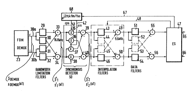
Referring now to Fig. 4 which is a circuit diayram of
-the present invention, the frequency division demultiplexer 23
receives the combined sequence of PCM pulses and separates this
se~uence into individual streams of such pulses for each of the
plurality of different channels l to L, inclusive. For each
channel, the demultiplexer 23 separates the digitalized signals
into first and second quadrature displaced streams of PCM pulses
over lines 30a and 30b. The irst stream of pulses over line 30a
are directed in parallel to a pair of bandwidth limitation -filters
29 and 30, and the second stream of PCM pulses, which are phase
displaced by 90 deyrees with respect to the first stream of
pulses, are directed in parallel over line 30b to bandwidth
limitation filters 31 and 32.
The bandwidth limitation filters 29-32 have complex
coefficients, that is, each has a complex-valued impulse response
~BB = hr + ihi, where
hr and hi are the real and imaginary components of the impulse
response.
The input signal to each of the bandwidth limitation
filters 29-32 from the frequency division demultiplexer 23 is a
complex time domain signal
S DEMU~kT) = Sr(kT) + jSi(kT), where kT is the sampling
,~, ., 1 0
12~08~
27371-1~30
instant with T the spacing of the samples and k an integer, ~Ihich
permits numbering of the sar.nples.
Filtering is performed by convolution, indicated by the
symbol *, resulting in the complex-valued output signal or se-
quence sl(kT)
s1(kT) = ~DEMUX(kT) * ~BB
= (Sr + iSi) * (hr ~ jhi).
Accordingly,
sl(kT) = (Sr * hr ~ Si * hi) ~ i(Sr * hi ~ Si
where (Sr * hr ~ Si * hi) is the real part of the output
and (~r * hi + Si * hr) is the imaginary part of the out-
put.
Thus the real part of the sequence sl(kT) is obtain-
ed by passing the signal Sr (30a) through the bandwidth limita-
tion filter 29 with impulse response hr and subtrac-tion from its
output the output of the bandwidth limitation filter 31 with
impulse response hi which is fed with the signal Si (30b).
The imayinary part of the sequence sl(kT) is obtain-
ed by passing the signal Sr (30a) through the bandwidth limita-
tion filter 30 with impulse response hi and adding to its outputthe output of the bandwidth limltation filter 32 with impulse
response hr which is fed with the signal Si (30b).
The filtered streams of pulses from quadrature displaced
~ilter 29 and 31 are subtractively combined in adder 33; and the
quadrature displaced streams of filtered pulses from filters 30
and 32 are additively combined in adder 34. The difference and
-- 11 --
~00~1
27371-180
sum PCM signals from adders 33 and 34 are obtained at the actuaL
output sampling frequency, in this particular case: 16.8 k~z.
The difference stream oE pulses is directed to demodulators 35 and
36; and the sum stream oE pulses are directed to demoduLator 37
and 3~. Demodulators 35-38 are components of a synchronous de-
modulator circuit SD that extrac-ts the carrier signals, shifts t'ne
center frequency fm of the spectrum to zero and produses the
envelopes a-t adders 39 and 40. SpeciEically, a difference signal
is obtained at adder 39 and a sum signal is obtained at adder 40,
after synchronous demodalation in a feedback loop.
The operation of the demodulator circuit SD can be
understood by considering the bandwidth limi-tation filters 29, 32
and 30, 31 to ha~e the transfer functions
cos 2~kfm/fSo and sin 2~kfm/fso~
respectively so that the filter blocks 29-32 operate as simple
digital multipliers. Thus, as shown in Fig. 4, the incoming real
and imaginary parts of the signal are sl(kT) are multiplied oy
the PCM samples of cos 2~kfm/fSo and sin 2~kfm/fSo.
These two real carriers of frequency fm are combined to form a
complex carrier
ej2~kfm/fSo = cos 2~kfm/fSo -~ j sin 2~kfm
The difference signal at adder 39 is then directed to
interpolation filters 43 and 44; and the demodulated sum signal is
directed to interpolation filters 45 and 46 where their sampling
frequencies are changed, for instance to 9.6 kHz. If tne demodu-
lation ~requency is selected to equal fm, the filter function
-- 1~ --
~"~
~LZ90~8~
27371-180
becomes symmetrical abou-t f=0 and the additional interpolation
filters 44 and 45 (shown by dashed lines) are not required.
The output of interpolation filter 43 (and 45 when
used), and the output of fiiter 46 (and filter 44 when used) is
connected to adders 49 and 50, respectively. Following interpola-
tion the resulting sum and difference signals at adders 49 and 50
are directed to the data (Ny~uist) filters 51, 52 and 53, 54,
adders 55 and 56. As in the case of the interpolation fiLters,
Nyquist filters 52 and 53 are not needed when the demodulation
frequency is equal to fm.
The outputs of adders 55 and 56 are coupled to a decider
circuit 47 which controls feedback channels 48 and 67. Feedback
channel 48 is connected directly to the interpolation fil-ters
43-46, and feedback channel 67 is connected to the synchronous
demodulator SD through a function generator having the transfer
characteristic
ej2~kfm/fso~ which generates a sine signal for
control of demodulator 36 and 37 and a cosine signal for control
of demodulators 35 and 38.
2~ The freq~ency fm is con-trolled via the feedback con-
nection 67 such that the spectrum S2', as is explained below in
connection with Fig. 6b, is centered at zero frequency. The feed-
back connection 48 from the decider circuit 47 to the interpola-
tion filter circ~it forces the interpolation filter to select t`ne
correct sampling instan-tly out of a number of possibilities.
The decision circuit 47 decides which data was trans-
~L29~81
27371-180
mitted. In the case of a QPSk modulation the output signal 6~ is
therefore just the sign of the output signal of the adder 5~. The
output signal 66 is just the sign of the output signal of the
adder 56.
A useful frequency control may be based in the case of a
QPSk modulation a four-phase Costas loop as described in [2], Fig.
11 .9 .
Timing recoveries are also well known, examples may be
found in [3~, [4].
~2~ F.M. Gardner: Phase Lock Techniques, John ~iley & Sons, 1979
[3] K.H. Mueller, M. Muller: Timing Recovery in Digital
Synchronous Data Receivers, IE~ COM-24, no. 5, ~ay 1976.
L4~ F.M. Gardner: A BPSk/QPSk Timing Error Detector for Sampled
Receivers, IEEE COM-34, No. 4, May 1986.
The operation of the circuit of Fig. 4 can be further
understood from a study of Figs. 6a and 6b and a comparison of
those figures with Figs. 5b and 5c, respectively. In Fig. 6a, Sl'
is the spectrum of the complex-valued output signal of the filters
29-32 of Fig. 4, and in Fig. 6b, S2' is the spectrum of the
complex-valued input signal of the interpolation filters 43-46.
As in the circuit of Fig. 3, the interpolation filters have real
coefficients and are used twice for the real and imaginary parts
of the time domain function corresponding to S2'.
Note that the spectrum S2 of the input signal to the
IPF is just a shiftet version of the spectrum Sl . Compared to
Fig. 5c there is no additional mirror spectrum tha-t appears.
- 14 -
~,f--
~9~81 27371-180
Compared to Fig. 5c the distance ~f' between two repeti-
tive spectrums is much greater. Thus, the filter degree of IPF
according to Fig. 4 (Fig. 6c) is correpondingly smaller than in
the case o the prior art.
Fig. 7 shows a simplified diagram of a slightly modi-
fied structure compared to Fig. 4, where the output signal of the
demultiplexer is fed into the bandwidth limitation fiLter w'hich
output is fed into the synchronous demodulator which output is fed
into t'he interpolation fiLter which output is fed into the pulse
s'haping filter ~hich output is fed in the decision circuit, but
where control signals for the timiny adjustment and frequency
correction are obtained from the output signals of the
interpolation filter, thus before the pulse shaping is performed.
An example -for a useful frequency control loop is in this
case a loop with the quadricorrelator as frequency discriminator
in conjunction wi-th a PLL as described in L5]. An example for a
useful timing loop is described in [6].
[5] David G. ~esserschmitt, Frequency Detectors for PLL
Acquisition in Timing and Carrier Recovery, IEEE COM-27, No.
9, Sept. 1979.
L6~ D-N. ~odard: Passband timing recovery in an All Digital Modem
Receiver, IEEE COM-26, ~o. 5, May 1978.
1~90~8~
27371-1~0
It will be understood that the above description of the
present invention is susceptible to various modifications, changes
and adaptations, and the same are intended to be comprehended
within the meaning and range of equivalents of the appended
claims.
16