Note: Descriptions are shown in the official language in which they were submitted.
1~:9~ 6
Description
OPTICAL PRESSURE-SENSING SYSTEM
Technical Field `~
This invention relates to optical pressure
sensors and, more particularly, to use of optical pressure
sensors for microphones, di~ferential pressure measure
ments, and gas density measurements, as well as structures
or mounting and combining such senEors in a unitary
system.
. .
Backqround Art
10A wide variety of physical parameters, such as
pressure and gas density, are measured with electronic
sensors. Although electronic sensors are satisfactory for
most applications, -there are many applicatîons that
preclude the use of such sensors. For example, electronic
pressure sensors often cannot be used in the presence~of
electromagnetic interference tEMI) since the~ EMI will
generate large voltages on either the components of the
sensor or the wires connecting the sensor to an external~
device. Many electronic devices for sensing physical
parameters are incapable of providing satisfactory results
in the presence of high magnetic fields, such a~s~, ~or
example, would be found adjacent transformers, motors and
the like. Other electronic devices Eor sensing a physical
parameter are effected by variations in other physical
parameters. For example, some electronic ga~s density
sensors are, in reality, electronic pressure sen`sors since
pressure is proportional to gas ~ensity ~or~a given
temperature or volume. However, the accuracy o~ such
sensors is greatly degraded by variations in temperature or
changes in the volume of the container for such gas.
In order to solve these and other problems
associated with electronic sensors, various optical devices
' ; ~ `' ~ ' ` ' '
~ 2~)166
Eor sensing physical parameters such as p~essure have been
devised. For example, U.S. Patent 4,487,206, to Aagard,
: describes a pressuxe sensor in which light is reflected
from one fiberoptic waveguide to another by a reflective
diaphragm. The amount of light reflected is a function of
the shape of the reflective diaphragm, which varies in
accordance with pressure. Similarly, U.S. Patent
4,210,029, to Porter, discloses a differential pressure
sensor in which light is reflected from one optical
waveguide to another by a reflector mounted on a flexible
membrane. The amount o:E light reflected from one waveguide
to the other is a function of the position of the
reflector, which is controlled by the applied pressure.
U.S. Patent 4,428,239, to Johnston, discloses a differen-
: 15 tial pressure sensor in which light from a common source is
reflected from opposite sides of a diaphragm which de~flects
as a function oE the differential pressure across the
diaphragm. The interference between the light reflected
from opposite sides of the diaphragm is detected and used
` 20 to indicate the differential pressure across the diaphragm.
: Fiberoptic pressure t~ansducers have also been
devised which can measure the absolute pressure at two
points using separate sensors. The differential or
relative pressure at these two points can then be
calculated by comparing the output of the two sensors in adifference circuit. In many cases, this scheme is not
: sa-tisfactory because of sensor drift or the problem of
exceptional bulk in the cable because of the need to
connect several transducers to the difference circuit.
Further, in some applications, where size constraints
exist, ~uch as monitoring the pressure in the heart and
other organs, it is desirable to have a single, compact
sensor for measuring differential pressure.
Other optical devices for meaCuring physical
3S parameters provide inadequate performance because they
: backscatter scatter excessive light at the interfaces
between the fiberoptic waveguide and other components.
- -
- , ~ . . . :
,
. : .
.
.
:~L29(~L66
Disclosure of Invention
It is an object of the invention to provide an
optical pressure sensor that is capable of accurately
S measuring differential pressure using a single fiberoptic
waveguide extending from the sensor.
It is another object of the invention to provide
an optical differential pressure sensor that receives
differential pressures through fluid conduits that may be
manufactured with xelative ease and which does not
interere with the deflection of a differential pressure
responsive diaphragm.
It is another object oE the invention to provide
an optical pressure sensor that can be used as an audio
micxophone.
It i8 still another object of the invention to
provide an optical pressure 6ensor that can be used ~o
measure gas density and that is internally self~compensat-
ing for temperature variations.
It is a still fur-ther object of the invention to
provide an interconnecting system for optical pressure sen-
sors that minimizes errors resulting from backscattering
and that allows several such pressure sensors to be
combined.
Brief Description of the Drawin~s
Figure 1 is a schematic showing an optical
pressure-~ensing system. ~ -
Figuxe 2 is a graph showing the reflectivity of
the pressure sensor used in the system of Figure 1 as a
~unction of the wavelength of light applied to the sensor.
Figure 3 is a graph of the reflectivity of the
pressure sensor of Figure 1 fox various resonant wave-
lengths of the pressure sensor.
Figure 4 is a schematic of a pxessure-sensing
system utilizing a ratiometric light-detection technique.
-
; : -
~ :: - ~. , -
:~ ~ ' ': ' ' '
' '"' ' / , :
, . ' ~ :
66
Figure 5 is a graph of the reflectivity curve o~
the pressure sensor used in the system of Figure 4 for two
different resonant wavelengths of the sensor plotted
against the frequency spectrum of the light incident on
5 the pressure sensor. ~ ;
Figure 6 is a graph showing the spectrum of light
reflected from the pressure sensor when the spectrum of the
incident light is symmetrically positioned about the
resonant wavelength of the pressure sensor~
Figure 7 is a graph of the spectrum of the light
reflected from the pressure sensor when the incident light
is centered at a wavelength that is larger than the
resonant frequency of the pressure sensor.
Figure 8 is a cross-sectional view of an optical,
differential pressure sensor.
Figure 9 is a cross-sectional ~iew taken a~long ~-
the line 9-9 of Figure 8.
Figure lO is a cross-sectiona~l view of an optical
pressure sensor specially adapted for use as a microphone.~
20~ Figure ll is a cross-sectional view taken along
the line ll-ll of Figure lO.
Figure 12 is a cross-sectional view oE an optical
; pressure sensor mounted for measuring the pressure of~ fluid~
in a pipe and in optiaal communication through a removable
coupling.
Figure 13 is a schematic showing the manner in
which light losses occur because of misalignment~s ~i~n a~
fiberoptic waveguide and a light-rerlecting surface.
Figure 14 is a schematic showing the use of~ a
lens to prevent light losses resulting from misali~gnments
of a ~iberoptic waveguide and a reflective pressure sensor.
E'igure 15 is a cross-sectional view of an optical
pressure sensor mounted in a releasable, low-loss coupling.
Figure 16 is a schematic of a conventional beam
splitter used with an optical sensor.
Figure 17 is a schematic of a beam splitter using
graded refractive index lenses
,:
3L290~66
~ igure 18 is a schematic of a beam splitter
utilizing a transparent block.
Figure 19 is a schematic showing another
embodiment of a beam splitter utilizing a transparent
block.
- .
Best Mode for Carrying Out the Invention
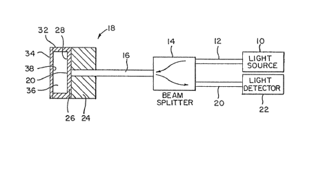
The basic concept of an optical pressure-sensing
system is illustrated in Figure 1. Basically, a light
source 10 generates input light which either may be
monochromatic or may be composed of a range of wavelengths
falling within one or more color bands. More specifically,
the light source 10 may be a laser or light-emitting diode
(LED) and it may emit light having a wavelength of 810 nm.
Input light from the light source 10 is coupled
through a first fiberoptic waveguide 12 of conventional
design to a first input port of a beam splitter 14,
described in greater detail below. A second fiberoptic
waveguide 16 extends from a second por-t of the beam
splitter 14. The beam splitter 14 functions to couple
light from the first fiberoptic waveguide 12 at the first
port of the beam splitter 14 into the second fiberoptic
waveguide 16 through the second port of the beam splitter
14. Light convey d through the fiberoptic waveguide 16
then reaches pressure sensor 18, described in detail below.
Basically, pressure sensor 18 modifies the spectrum of
light incident on the sensor 18 and reflects back the
spectrally modulated light. For example/ the pressure
sensor may increase input light at one wavelength with
respect to ligh-t at another wavelength~ The spectrally
modulated light re~lected from the pressure sensor 18 is
then coupled to the second port of the beam splitter 14
through ~iberoptic waveguide 16. Beam splitter 14 then
functions to couple the reflected light to a third ~iber-
optic waveguide 20 through a third port oE the beam split-
ter 14. The reflected light coupled through fiberop-tic
'~
: ~ , . . .
. ~
::' ~ : , ' : '
~, ~2~0~66
waveguide 20 is then sensed by a light detector 22, which
may be, for example, a conventional photodetector.
The optical pressure sensor 18 may include a
support 24 through which the fiberoptic waveguide 16
5 extends. The support 24 carries a substrate 26 consisting
of a base 28 having a planar surface 30 surrounded by
sidewalls 32. The base 28 is preferably circular and the
sidewalls 32 are preferably cylindrical. ~ resilient
diaphragm 34 is bonded to the edges of the sidewalls 32 to
10 form an airtight cavity 36. ~lternatively, the sidewalls
32 may be integrally formed with the diaphragm 34, and the
sidewall 32 may be bonded to the substrate 26. The inside
surface 38 of the diaphragm 34 is planar and it is parallel
to the planar inside surface 30 of the base 28. The
15 thickness of the airtight cavity 26 (i.e., the di stance
between the inside surface 30 of the base 2~ and the inside
surface 38 of the diaphragm 34) is selected so tha~ the
input light incident through fiberoptic waveguide 16
resonates in the cavity 36. Cavity 36 thus forms an
20 airtight optical resonator. As is well understood in the
art, the resonant frequency of thé cavity 36 is dependen~
upon the thickness of the cavity 36. Thus, deflecting the
diaphragm 34 inwardly or outwardly alters the thickness of
the cavity 36 and hence its resonant frequency. The
25 diaphragm 34 is formed by a resilient material so that it
deforms inwardly when the external pressure is greater than
the pressure in the cavity 36. Diaphragm 34 deflects
outwardly when the external pressure is less than the
pressure in the cavity 36. The theory of operation of the
30 pressure sensor is described in greater detail below.
In order to maximize the spectral modulation, the
i nsi de surface 30 of the base 28 is preferably provided
with a partiall~ light-transmissive, partially reflective
coating, while the inside surface 38 of the diaphragm 34 is
35 provided with a reElective coating.
The theory of operation of the optical pressure-
sensing system depends upon the characteristics of the
: : . , , : : , ~: . : ,
.
.
~,, ' , ~ '
6~
reflectivity curves of the sensor 18 in response to input
light. Basically, the rerlectivity curve undergoes a
shift, known as a "microshift," when the resonant frequency
of the cavity 36 shifts responsive to small pressure-
5 induced deformations of the diaphragm 34. The reflectivity
(R) of the optically resonant cavity 36 is given by the
e~uation:
R = l-s2/((l-r)2 + 4rsin2(theta))
where s = (sl s2)-5 and r = (rl r2) 5. The quantities
sl~ s2 are, respectively, the transmittances of reflective
surfaces 30, 38, while rl, r2 are, respectively, the
reflectances of reflective surfaces 30, 38 as seen from
within the cavity 36.
The angle theta in the sine term in the above
equation is known to be given by:
theta = 2(pi)nt cos(phi)/lambda + e
where: n = the refractive index of whatever is in the
cavity 36 be~ween reflective surfaces 30/ 38;
t = the distance between reflective surfaces 30,
20 38;
phi = the angle of light reflection between reflec~
tive surfaces 30, 38;
lambda = the wavelength of input light incident in
optically resonant cavity 36; and
25e = any phase shift caused by reflection from
either reflective surface 30, 38.
A typical reflectivity curve 40 is il].ustrated in
Figure 2. 1'he reflectivity R is a periodic function of the
wavelength of the input light, as can be seen by examining
the equation set for-th above. Specifically, it can be seen
that the reflectivity R is a periodic function of the param-
eter group nt cos ~phi)/lambda. The ma~imum reflectivities
thus occur at nt cos (phi)/lambda = (2m + l)/4, while the
minimum reflectivities occur at nt cos (phi)/lambda = m/2;
where m is the cycle number and is 0 or a positive integer.
It is thus seen that adjacent maxima and minima are
.. :: : ~ .: .
::
,;
' , , ' ` ''' ' ". I " ' ' '
, " ~ .
30~l6~
separated from each other by exactly one-quarter oE the
parameter group nt cos (phi)/lambda. Insofar as the thick-
ness T of the cavity 36 varies according to the differen-
tial pressure across the diaphragm 34, it can be seen that
5 the parameter group nt cos (phi)/lambda will vary in
accordance with the applied pressure.
Figure 3 illustrates the microshirt of the
reflectivi~y curve 40 to positions 40' and ~0'' responsive
to variat.ions in the thickness T of the cavity 36. In
10 par-ticular, the reflectivity curve 40 shifts -to the left
with respect to the wavelength Ll of input light from light
source 10 to the reflectivity curve 40' when the thickness
T of the cavity 36 is reduced respoDsive to increases in
the external pressure. Similarly, the reflectivity curve
40 is shif-ted to the right with respect to the wavelength
Ll to become reflectivity curve 40'' when the thickness rr
of the cavity 36 increases responsive to decreases in the
: external pressure. The distance between adiacent maxima:or
adjacent minima is termed a "cycle length." It will be
apparent from an examination o~ Figure 3 that a given value
of reflectivity will occur at two points for each cycle of
the reflectivity curve. Thus, in order to achieve a unique
reflectivity for a given pressure, the optical pressure
sensor must be kept within a range or "operating segment"
of one-half resonance cycle extending between an adjacent
maxima and minima. For example r curve A-C and C-B each
constitute an operating segment in one resonance cycle of
reflectivity curve 40.
Assuming that the light source 10 emits input
light having a wavelength Ll, it will be apparent that when
the reflectance curve 40 shifts to the position 40' respon-
sive to a decrease in external pressure, the amplitude of
the spectrally modulated input light received at light
detector 22 will decrease. Similarly, when the
reflectivity curve 40 microshiEts to the position 40''
respon.sive to decreases in the external pressure, the
amplitude o~ the ~pectrally modulated light sensed at
,~ .,
: ' ; ` , '
: ' ~
: .
~290166
detector 22 will increase. As mentioned above, light
detector 22 may be a variety of light-sensitive devices,
such as a photodetector, which, when connected in known
circuits, may produce an electrical output having a
5 magnitude that is proportional to the intensity of the
incident light. Thus, the light detector 22 may produce a
voltage that is proportional to the pressure external to
the cavity 26~
~lthough the embodiment illustrated in ~igure 1
will produce an output that is proportional to the e~ternal
pressure, it suffers from a number of potential limitations
because the intensity of the output light applied to the
light detector 22 may vary Eor reasons othex than micro-
shifts of the reflectivity curve 40. For example, the
intensity of the light received by the light detector 22
will vary in accordance with variations in the intensity of
the input light generated by the light source 10. Also,
variatlons in the losses and leakages in the fiberoptic
waveguides 12, 16, 20 will result in variations in~the
light a-t the light detector 22. For these reasons, a ratio-
metric system, illustrated in Figure 4, may be used as the
light detector 22. In the ratiometric system, output light
from the beam splitter 14 and waveguide 20 is incident on a
second beam splitter 50, which passes a portion of the
incident light to a short-pass optical filter 52. The
short-pass optical filter 52 preferentially transmits light
having a wavelength that is shorter than a predetermined
wavelength. The shorter wavelength light Erom filter 52 is
converted to a first electrical signal by a light detector
54, which may be a conventional photodetector circuit. The
output of the light detector 54 is then boosted by
amplifier 56.
The portion of the light reflected by beam
splitter 50 is incident on a long-pass optical filter 60.
The long-pass optical filter 60 preferentially transmits
light having a wavelength longer than a predetermined value.
The lony wavelength light passing through filters 60 is
:::
~: :
.. . . . .
,.
~L2~l66
converted to a second eletrical signal by a light detector
62. The output of the light detector 62 is then boosted by
an amplifier 66.
The ampliEied first and second electrical signals
5 from amplifier 56, 66, respectively, are applied to a con-
ventional divider circuit 68. Divider circuit 68 generates
an output that is proportional to the ratio of the ampli-
tude of the signal of the output of amplifier 56 to the
amp]itude of the signal at the output o~ amplifier 66. As
10 explained in greater detail below, the output of the
divider circuit 68 is an electrical signal that is propor-
tional to the pressure measured by the pressure sensor 18.
It will be apparent that any variations in the intensity of
the light from the light source 10 as well as variations in
the losses or leakage in the fiberoptic waveguides 12, 16,
20 will result in equal variations in the light at both
light detectors 54, 62. As a result, the output of the
divider circuit 68 is unaffected by such variations. ~
The embodiment illustrated in Figure 4 must
utilize a light source 10 that emits input light havlng
either at least two wavelengths or a range of wavelengths.
In contrast, the light source 10 of the embodiment of
Figure 1, preferably emits light having a single or rela-
tively narrow band of wavelengths. The frequency spectrum
of one such light source 10 is illustrated in Figure 5 as
curve 86. Also illustrated in Figure 5 is a portion of the
reflectivity curve 40, which is selected to have a resonant
wavelength or maxima coinciding with the wavelength of the
highest intensity light from the light source 1~. However,
it will be understood that the resonant wavelength of the
cavity 36 and the wavelength of highest intensity from the
light source 10 need not coincide. When the resonant wave-
length coincides with the wavelength of maximum intensity
from the light source 10, the output light incident on the
beam splitter 50 will have the spectrum illustrated in
Figure 6. Since the light having wavelengths longer than
wavelength h2 is modified by the reflective curve 40 to the
'
--- . - ~ - . .
.
.
~ ~0166
11
same extent as the light having a wavelength shorter than
the wavelength L2, the spectrum of light incident on the
beam splitter 50 is symmetrical about wavelength L2, as
illustrated in Figure 6. If the cutoff wavelength of the
short wavelength filter 52 and the long wavelength filter
60 are selected at L2, the output from light detector 54
will have an amplitude equal to the area F, while the
output of light detector 66 will have an amplitude equal to
the area G. Under these circumstances, the output of the
divider circuit 6~ will be unity. A similar result will be
achieved even if the cutoEf wavelengths for the filters 52,
60 do not coincide, as long as the filters 52, 60 preferen-
tially pass some wavelengths of the light from light source
lO to a greater degree than other wavelengths.
In the event that the pressure measured by the
pressure sensor 18 increases, the reflectivity curve illus-
trated in Figure 5 will shift from the position 40 to the
position 40'. The spectrum 86 of the light from the light
source lO will thus be altered to the spectrum illustrated
in Figure 7. In other words, since the reflectivity curve
40 has shifted to the position 40', li~ht having a wave-
length shorter than L2 is reflected to a degree greater
than the reflection of light having wavelengths greater
than a wavelength L2. As in the example given above, light
having a wavelength shorter than L2 is preferentially
applied through short wavelength Eilter 52 to the light
detector 54. The output of light detector 54 will thus
have an amplitude corresponding to the area H. Light
having a wavelength greater than 12 is preferentially
applied through long wavelength eilter 60 to li~ht detector
62 so that light detector 62 generates an output having an
amplitude corresponding to the area I. As a result, the
output of divider circuit 68 will be equal to the ratio of
area H to area I.
It can be noted from examining Figures 5-7 that
the embodiment of Figure 4 will operate for microshifts of
up to plus or minus one-half operatin~ cycle. The total
.
'
)16~
12
operating segment of the embodiment o~ Figure 4 is thus a
complete operating cycle, in contrast to the one-half
resonance cycle operating segment of the embodiment of
Figure 1. The embodiment of Figure 4 thus not only cancels
5 out spurious variations in the detected light, but it also
has a greater dynamic range.
Another embodiment of a pressure sensor is illus-
trated in Figures 8 and 9. Components of this embodiment
that are found in the embodiment of Figure 1 are given
1~ identical reference numerals for clarity of explanation.
Thus, in the embodimen-t of Figures 8 and 9, the fiberoptic
waveguide 16 extends through support 24 and terminates at a
substrate 26 having a base 28 with a planar inner surface
30 surrounded by sidewalls 32. As in the embodiment of
15 Figure 1, a resilient diaphragm 34 having a planar inner
surface 38 is secured to the sidewalls 32 to form an
airtight cavity 36. As explained to this point, the
embodiment of Figure 8 is identical to the embodiment of
;~ Figure 1.
The embodiment of Figure 8 is specifically
adapted to measure diEferential pressure. Accordingly, it
includes a second substrate 100 having a base 102 with an
lnside surface 104 that, unlike the inner surface 300 of
substrate 26, need not be planar. Sidewalls 106 are
secured to the surface 108 of the diaphragm 34 to form an
airtight cavity.
With reference also, now, to Figure 9, the
airtight, optically resonant cavities 36, 110 communicate
with respective pressure ports 112, 114 through respective
fluid conduits 116, 118. While the routing of a fluid
conduit from khe cavities 36, 110 to respective pressure
ports 112, 114 might seem relatively straightforward, care
must be taken to prevent the fluid conduits from affecting
either khe deflection characteristics of the diaphragm 34
or the optical properties of the cavities 36, 110 and the
substrate 26. Additionally, because the cavities 36, 110
; are extremely thin, i.e., on the order of one micron, it is
.
: ~ :
:~ ' .' ' ~ . ," '
1~9~ 6
difEicult to fabricate fluid passages to the cavities 36,
110 without adversely af-fecting the operation oE the sensor.
However, these problems can be overcome by ~orming a radial
projection or arm 120, 122 integrally with each of the
cavities 36, 110, respectively. When the diaphragm 34 is
secured to the sidewalls 32, 106 of the substrates 26, 100,
respectively, the radial projections 120, 122 are seaIed
from the external environment. It is then ~ relatively
simple matter to bore or otherwise form holes 116, 118 in
the respective substrates 28, 100 that extend Erom the
respective pressure ports 112, 114 to the projections 120,
122.
- In operation, the deflection of the diaphragm 34
is determined by the differential pressure on opposite
sides o~ the diaphragm 34 in the cavities 36, 110. Thus,
when the pressure in cavity 36 is greater than the pressure
in cavity 110, the diaphragm 34 bows outwardly away ~rom
the fiberoptic waveguide 16. When the pressure in the
cavity 36 is less than the pressure in the cavity llO, the
diaphragm 34 bows inwardly toward the fiberoptic waveguide
16. As in the embodiment of Figure 1, deflection of the
diaphragm 34 causes microshifts in the reflectivity curve
from the sensor. In order to maximize the sensitivity of
the sensor, the planar inside surface 3U of the substrate
28 is preferably coated with a partially reflective,
partially light-transmissive mirror and the surface 38 of
the diaphragm 34 is coated with a reflective material. In
order to prevent light from being reflected into the
fiberoptic waveguide 16 from the inside sur~ace 104 of the
substrate 100, the sur~ace 104 is made non-reflective
through one o~ a variety oE techniques. For example, the
surface 104 may be roughened (as shown), or it may be
provided with a light-absorptive surface. Since the second
airtight cavity 110 does not function as an optical
resonator, it is not necessary for the surface 104 to be
planar.
, :
- ,
: ~ '
,
~.' : .. : :. . . . . . . .
.
:, : . .
~ 0~66
14
One highly advantageous feature of the differen-
tial pres~ure sensor is that it requires only a single
Eiberoptic waveguide 16 extending to the sensor. Conven-
tional prior art sensors utilize a pair of fiberoptic
5 waveguides extending to the sensor which make the sensor
more bulky and thus less useful in certain applications,
such as internally monitoring blood pressure. The use of
two fiberoptic waveguides also requires additional
components to process the light coupled through both
10 fiberoptic waveguides.
The optical differential pressure sensor
illustrated in Figures 7 and 8 may be fabricated using a
variety of techniques. However, the small thickness of the
cavities 36, 110, both in absolute terms and in relation to
15 the diameter of the diaphragm 34, presents~special
fabrication problems that must be dealt with. Normally,
the cavities 36, 110 will have a thickness of about 1
micrometer while the diameters of the cavities 36, 110 will
be about 200-1,000 micrometers. Conventional techniques
20 for bonding using glue cannot be used to secure the
diaphragm 34 to the substrates 28, 100 because the high
capillary pressure in the cavities 36, 110 draw~ glue into
the cavities. Furthermore, the bond betwee~ the sidewalls
32, 106 and the diaphragm 34 should preferably be as strong
25 as the materials themselves. It has been found that an
ionic bond, such as an anodic bonding technique, may be
used when the diaphragm 34 is made of silicon and the
substrates 28, 110 are of a compatible glass-like material.
Although the pressure sensors may be ~abricated
30 using a variety of manufacturing techniques, one specific
manufacturing technique i~ described below. The starting
point is a glass wafer .011 ~ .001 inch thick of fused
, silica or a low-expansion glass such as Corning ~7740.
Both surfaces of the waEer are ground and polished to an
optlcal finish. The glass wafer will form the substrates
26 of the sensors 18.
* J~ie ~r~c~ r k
. ` .
. . ~ ,
. . . ... . . ~ . ~ ,,
~.2~0~6~
The surfaces of the glass wafer are first cleaned
by washing the glass wafer in hot, soapy wa-ter; rinsing it
with clean water; etching and polish.ing it for one minute
in a buffered HF solution composed of four parts of a
5 mixture of 3 ml water and 2 g NH4F plus one part 48% HF
solution; rinsing it again; and then baking it at 300C for
one-half hour.
Using a conventional vacuum deposition process~ a
layer of chrome 200 Angstroms thick is then depos.ited on
10 the glass wafer. This chrome provides a good adhesion
surface for the subsequent application of photoresist to
the gl.ass wafer.
Photoresist, such as Microposit 1400-27 photo-
resist made by the Shipley Company, located in Newton,
15 Massachusetts, is then spin-coated on the chrome surface of
the glass wafer at 3000 rpm; after which the coated glass
wafer is baked at 90C for one-half hour.
Using conventional techniques, a photoresist mask
is then prepared having an array of circles of a diameter
e~ual to the desired diameter of the cavi-ty 36, for
: example, 200 microns. The mask is aligned with the
photoresist-coated surface of the glass wafer; and the mask
and glass wafer assembly is then exposed. The exposed
coated glass wafer is then developed with photoresist
developer, such as Microdeposit 35ICD-23 developer, made by
the Shipley Company; rinsed in water; and dried.
As a resultj unprotected circles.200 microns in
diameter in the photoresist are left on the gIass wafer.
The chrome within the unprotected circles in the photo-
3~ resist .is lifted off with a chrome etch solution composedof one part HC~ and one part glycerine, leaving circles of
unprotecked gla~s 200 microns in diameter on the sur~ace of
the glass wafer.
The circles of unprotected glass on the glass
wafer are then etched Eor about 20 minutes at 69F with
said buEfered HF solution to produce the cavity 36 in the
subtrate 26 r which may be 1.27 microns deep. Even though
~ T ~I de~ rk
"~
, . .. .
- :~ , ';
. , ~ . -
~l2~0~L66
16
the planar surface 30 of the substra-te 26 is formed by
chemical etching, it is still flat enough to form an
adequate reflective surface 30 for the sensor's optically
resonant cavity 36.
Using conventional vacuum deposition techniques,
a layer of titanium dioxide 200 Angstroms thick is then
deposited on the surface 30 of each cavity 36 to increase
the reflectivity of the surface 30. This increases the
intensity of the modulation of the output light of the
sensor 18. The remaining photoresist is then removed with
acetone, and the chrome on the glass wafer is then removed
with the chrome etch solution. Finally, -the gla~s wafer is
washed in water and air dried.
When the pressure sensor 18 is to be used ~or
measuring absolute pressure, the cavity 36 must be evacu-
ated. Although there are many ways in which the cavity 36
can be evacuated, it is preferred to use a getter structure
in the form of a ring of deposited layers of chrome and
iron in the bottom of each cavity 36 to absorb residual
gases or subsequent outgassing in cavity 36~after the
initial evacuation of cavity 26 is performed.
The getter rings for cavity 36 in the glass wafer
is prepared by first baking the glass wafer (prepared as
described above) at 125C for one-half hour, spun-coated as
before with photoresist, and baked again at 90C for
one-half hour. rrhen~ using conventional techniques, a
second photographic mask is prepared having an~array of
donut-shaped masks. Since the cavity 36 may be 200 microns
in diameter, for example, the corresponding donut-shaped
mask in the cavity 36 may have an inner diameter o~ 140
microns and an outer diameter oE 190 microns. The donut-
shaped masks on the second photographic mask are then
aligned with the cavity 36 in the glass wafer; and the mask
and glass waver assembly is exposed, as before. The glass
wafer is then7 as before, developed and rinsed; and then
baked at 90C for one-half hour. This leaves an unpro-
~ected, donut-shaped hole in the photoresist on the surface
:
.
:. :
.
L66
17
30 of substrate 26 having an inner diameter of 140 microns
and an outer diameter of 190 microns.
Using conventional vacuum deposition techniques,
a layer of chrome 2Q0 Angstroms thic]c is deposited on the
entire glass wafer, followed by a layer of iron 800 Ang-
stroms thick being deposited on the layer of chrome. The
chrome helps the iron, which is the actual getter material,
to adhere to the glass wafer. Then the glass wafer is
placed in acetone and agitated with ultrasound. This
1~ removes the remaining photoresist and also removes the
chrome and iron/ but only the chrome and iron which were
over said remaining portions oE photoresist. Finally, the
glass wafer is washed with detergent, rinsed with water,
and dried.
The resulting getter structure comprises a donut-
~haped ring of the deposited chrome and iron layers with~an
inner diameter of 140 microns and an outer dia~eter of 190
microns centered on the surface 30 of the substrate 26.
The getter ring leaves a clear central portion 40 microns
in diameter in the bottom of each cavity 36 through which
light can pass.
The diaphragm 36 covering the cavity 36 may be
formed from a silicon wafer 3 inches in diameter, about
.018 inch thick and etch-stopped with 102 boron atoms/cc3
at a depth of 4.0 microns, as sold by Diffusion Technology,
Inc., of Milpitas, California 95035. Thus the silicon
wafer comprises an etch-stopped layer 4.0 microns thick
supported by a silicon substrate of much greater thickness.
The bondiny procedure preferably utilizes an
anodic bonding technique, as mentioned above, because glues
and adhesives would be drawn into the relatively thin
cavity by capillary action. The etch-stopped side of the
silicon wafer is provided with a layer of silicon dioxide
about 200 Angstroms thick. The silicon dioxide is formed
on ~he wafer by baking it in an oven at 900C for one hour
in order to increase the subsequent adhesion of the glass
wafer to it, as described subsequently. Next, the glass
: -
- , .. .
: ;: , :. ..
,: .. ~
` ' ` ` ~
~2~90~66
18
and silicon wafers, which have been prepared as previously
described, are cleaned with warm~ soapy water; cleaned in
an ultrasound bath for about 15 minutes; rinsed with water;
rinsed with alcohol; cleaned with alcohol; rinsed with
alcohol; and finally, air dried. I~he etch-stopped layer of
the silicon wafer is then placed on and aligned with the
surface of the glass wafer in which the cavity 36 has been
formed to produce a silicon and glass wafer sandwich. The
silicon and glass wafers are bonded together by first being
placed in a conventional vacuum chamber with a positive
electrode in electrical contact with the outer surface of
the silicon wafer and with a negative electrode in elec-
trical contact with the outer surface of the glass wafer;
after which the vacuum chamber is evacuated to about
6 x lO 6 torr for one hour. The silicon and glass wafer
sandwich is then heated by a heater in the vacuum chamber
to a temperature of 500C, at which it is maintained.
While the assembly is at this temperature, a bonding
voltage is appIied to the positive and negative electrodes.
The bonding voltage is ramped from 0-800 VDC, maintained at
800 VDC for about 8-lO minutes until tbe bonding current is
stabilized, and then turned off. At this time, the silicon
and glass wafers are now bonded together with a fluid-tight
seal, the sil~con dioxide layer on the silicon wafer aiding
in the bonding process. If getter rings have been formed
in the cavity 36, the temperature of the now bonded silicon
and glass wafer sandwich is maintained at 500C for an addi-
tional one-half hour to activa~te the getter rings. Next,
the heater in the vacuum chamber is turned off; and when
the silicon and glass wafer sandwich has cooled to about
300C, the vacuum in the vacuum chamber i.s released. The
bonded silicon and glass wafer sandwich is removed from the
vacuum chamber when it has cooled to about 200C.
After the silicon and glass wafer sandwich is
removed from the vacuum chamber, 70-80% of the thickness of
the silicon substrate of the silicon wafer is removed by
mechanical polishing. Next, an EDP etchant solution is
~ .
.~
' .
i6
19 ~,:
prepared co~posed of 8 ml water, 17 ml eth~lenediamine, and
3 g pyrocatechol. The EDP etchant solution is heated to
approximately 115C and used to chemically etch the pure
silicon substrate away, leaving only its etch-stopped -
layer, about 4.0 microns thick, which is bonded to the
glass wafer that forms the substrate 26. The 4.0-micron
thickness is determined by periodically checking the
thickness of the silicon remaining during the etching
process, such as by measuring light transmission through
the silicon.
As mentioned above, a Iight-reflecting coating is
preferably applied to the surface 30 oE substrate 26 and
the inner surface 38 of the diaphragm 34. A light-absorb-
ing coating is also preferably applied to the outer surface
of diaphragm 34 and surface 104 (Figure 8) of substrate 100.
The light-absorbing coating may be ~ormed by using conven-
tional vacuum deposition techniques to deposit two~or more
alternating layers of chrome and silicon on the outer
surface~of the diaphragm 34. A layer of chrome about 25
20 Angstroms thick is first deposited, ~ollowed by a layer of i~ ;
silicon about 100 Angstroms thick. The purpose of the
light-absorbing coating is to prevent external light ~rom
entering cavity 36 through diaphragm 34 and to prevent
light transmitted through the cavity 36 into diaphragm 34
from reentering the cavity 36 from the diaphragm structure
34. The reflective coating may be a material having a high
refractive inde~, such as TiO2.
The optical pressure sensor can be specially
adapted or use as a microphone to respond to variations in
30 pressùre occurring at audio Ere~uencies. One embodiment of
an optical microphone employing an optically resonant
cavity is illustrated in Figures 10 and 11. As with the
embodiment of Figures 1 and 2, the microphone 140 includes
a support 142 through which a conventional fiberoptic
waveguide 144 extends. A substrate 146 is mounted on the
support 142, with its lower surface contacting the end o~
the ~iberoptic waveguide 144. The substrate 146 includes a
: ' ` ' . ' , ' ', , , , '
~Z~ i6
base 148 having an inside surface 150 surrounded by
sidewalls 152. A resilient diaphragm 154 is bonded to the
sidewalls 152 in the manner described above with reference
to the differential pressure sensor of Figures ~ and 9.
5 The substrate 1~6 and diaphragm 154 together form an
airtight cavity 156. The cavity 156 communicates with an
external vent 158 through a radial projection or extension
160 of the cavity 156 in the same manner as described above
with reference to Figures 8 and 9. For the reason
lO explained below in greater detail, a pedestal 162 projects
upwardly from -the surface 150 of the substrate 146 into the
cavity 156. The pedestal 162 has a planar surface 164 that
is spaced close to the inside surface 166 of the diaphragm
- 154.
It has been found that a pressure sensor such as
illustrated in Figure 1 is not sufficiently sensitive for
use as a microphone. This lack of sensitivity exists
because diaphragm movement compresses the air inside the
cavity, thus, in fact, making it a spring that restrains
20 the deflection of the diaphragm. In order to improve
sensitivity, the cavity must be vented through projection
160 and vent 158, thereby allowing relatively free movement
of the diaphragm 154. However, the design of the venting
structure is somewhat critîcal. If the vent too easily
25 couples pressures waves into the cavity 156, the pxessure
waves will be received equally on opposite sides of the
diaphragm 154. Under these circumstances, the diaphragm
154 will not deflect responsive to such pressure waves.
If, however, the vent structure does not allow suEficient
30 coupling of a pressure wave to the cavity 156, then it is
eEfectively absent, thus reducing sensitivity.
Even if the pressure sensor of Figure 1 was
provided with a vent, sensitivity can be unacceptable
because the optical properties of the sensor re~uire that
35 the spacing between the inner surface of the substrate and
the inner surEace of the diaphragm be very small. Since,
for best optical performance, the thickness of the resonant
', ...
- ,
1;~90~66
21
cavity should be about one micrometer, movement of the vent
air through the cavity can be restricted by this small
dimension. In fact, viscous flow forces resulting from the
small thickness of the cavity are the limiting Eactor in
5 the high end frequency response of a pressure sensor. In
order for the microphone 14~ of Figures 10 and 11 to have a
frequency response that e~tends well up into the audio
range, it is necessary for the thickness of -the cavity 156
to be large enough to allc,w the free flow of vent air in
10 the cavity 156. However, a thick cavity 156 does not
: provide ade~uate opticai. performance. In order to achieve
: the good optical performance of a thin resonant cavity 156,
while also achieving the good pneumatic performance of a
thick optical cavity 156, most of the cavity 156 is made
15 relatively deep to minimize the viscous fLow forces
:
opposing movement of the vent air. However, the pedestal ~ ~.
162, with its planar sur~ace 164, is spaced sufficiently
~: close to the surface 166 of the diagphragm 15~ to provide
~ good spectral modulation performance. Since the pedestal:
.~ 20 162 occupies only a small portion of the cavity 156, it
does not impede the flow of vent air through the cavity
156. `
It has been found that the sensitivity of the
microphone is reIatively low for large spacings between the
surface 164 o~ the pedestal 162 and the surface 166 of the
diaphragm 1S4. As pedestal/diaphragm clearance is
decreased, microphone sensitivity increases and then once
~: again decreases as the pedestal/diaphragm clearance
approaches zero. The optimum pedestal/diaphragm clearance
30 i9 generally equal to on the order of several wavelengths
o light ~rom the lig~t source 10~ The microphone illus-
trated in Figures 10 and 11 is Pabricated in substantially
the same manner as described above with reference to the
di~ferential pressure sensor o:E Figures 8 and 9.
In order to ensure a frequency re~ponse extending
to at least 10 KHz, the cav.ity may have a diameter of less
than 1 millimeter and a thickness of about 1.5 micrometers.
.,
:
: ; . - . , :
. .
~, . ,
.~, . .
~2~
The embodiment of the pressure sensor illustrated
in Figure 1 may also be used as a gas density sensor. "Gas
density" is de~ined as the number o~ gas molecules per
volume, independent of such factors as pressure and -tempera-
5 ture. In some industrial processes, it is important tomeasure gas density. For example, in electrical switch
gear or electrical transmission lines, an insulating gas
(typically SF6) is used as an insulator. As the tempera-
ture increases, the gas pressure in the closed ~essel
containing this gas increases. As the temperature
decreases, the gas pressure decreases correspondingly~
Conventional gas density monitoring e~uipment must measure
both pressure and temperature and then interrelate these
two physical parameters to each other to sense a reduction
I5 in gas density resulting ~rom a leak in the vessel. The
inventive optical pressure sensor can be used to sense the
density of gas directly in a manner that is insensitive to
the temperature of the gas.
The inventive gas density sensor is based on
filling a small optically resonant cavity with a gas. The
cavity is, in part, formed by a resilient diaphragm so that
the diaphragm deforms responsive to the number of molecules
per volume (nor pressure) in a closed container that
contains the same gas that is inslde the optically resonant
cavity. The pressure sensor 18 (Figure 1) can be modified
for use as a gas density sensor. The pressure sensor 18 is
placed in a closed vessel containing the gas whose density
is to be measured, and the cavity 36 of the sensor 18 is
filled with the same gas bein~ monitored. Moreover, the
pressure of the gas in ~he cavity 36 at a given temperature
is made equal to the pressure of the gas in the vessel at
that same temperature. Thus, as the temperature in the
vessel containing the gas increases, the gas in the optical
resonator cavity 36 increases accordingly. As a result,
the differential pressure across the diaphragm 34 remains
at zero. However, if a leak in the vessel occurs, the
dens1ty of the gas in the vessel decreases, thereby
.
. . .
.
~2~66
decreasing the pressure outside of the cavity 36, which
causes the diaphragm 34 to bow outwardly. The increased
thickness of the cavity 36 then produces a microshift of
the reflectivity curve which is sensed by the light
detector 22, as explained above.
The operation of the gas density sensor can be
understood by assuming that the diaphragm 34 is very thin
and that diaphragm stiffness is negligible. If the
internal gas fill pressure of the sensor 18 exactly matches
the pressure of the monitored volume, the diaphragm 34 will
be Elat. As temperature changes, the internal and
monitored pressure will both change keeping the diaphragm
34 flat. If a leak in the monitored volume does occur, the
diaphragm position will change, reflecting a change in the
I5 monitored gas density.
An important feature of this gas density sensor
is that, in addition to having the same gas in the cavity
;: 36 and in the monitored volume, it can operate with
different gases inside the cavity 36 and in the sensed
20: volume. Additionally, it can operate without a significant
temperature coefficient even with different gas pressures
in the cavity and sensed volume.
The change in volume for a cavi-ty covered by a
; diaphragm is:
: 25
: a v = ap (l-ljm2)a~ (Equation 1)
16 E t3
where: aP = Pe ~ Pi, differential pressure
Pe = external pressure
Pi = internal pressure
m = inverse of Poisson's ratio
a = diaphragm radius
E = Young's modulus of diaphragm
t = diaphragm thickness
:: :
-~: ' " , " ' ' `'
: . . : :: :'
.
16~;
24
Initial cavity volume is:
VO = a2h + ~P~ l/m2? a6 tEquation 2)
16 E t3
Where: h = cavity depth
Po = initial differential pressure
:
With no gas leaks, as temperature changes, the pressure
external to the cavity will change as dictated by the ideal
gas law.
Pe = Po Ti/To (Equation 3)
Where: Po = initial external pressure
To = initial temperature
Ti - new temperature
the internal cavity pressure will become~
P~i = (Ps Ti/To) / (1 + (~V/Vo))) (Equation 4)
Where: Ps = initial "set" pressure for cavity gas
::::: :
At this poin~t it can be seen that for Ps = Po~av =: O for~
all values of temperature. That is for a fill pressure
equal to the exter~nal pressure, no diaphrag~ deflection is
experienced for any temperature. ~This~ is because~the~
pressures on both sides of the diaphragm rise and fall
identically with temperature.
If Po ~ Ps an initial deflection exists:
VO = -~ (Po-Ps) ~l-l/m2) a6 (Equation 5)
16 E t3 ~ ~ ~
~: ::: :: :
. ~ ~
- ~2~9~166
when the temperature changes, volume of the cavity 36 can
be obtained by solving the coupled equations (1), (3) and
(4) above. With the assumption that the sensed volume is
much larger than the sensor cavity 36, an expression can be
5 obtained. To make a true gas density sensor (not a
pressure sensor) the change in volume should be zero for
any change in temperature. The change in volume can be
made arbitrarily small by proper selection of sensor
parameters. Because the fractional volume change is:
~V _ ~(Po~Ps) ~ 1/m2) a~ (Equation 6)
V 16 L E t3 h~
It can be seen that for a sensor with a thin
15 diaphragm 34, shallow cavity, large radius, and high
initial pressure, the volume change can be minimized.
Evaluating the volume change for a 60C temperature range,
it is found to be less than 1% for a gas density sensor _
with an etched silicon diaphragm with a l~m diameter.
~0 The embodiments illustrated in Figures 1-10
utilize a fiberoptic waveguide that extends through a
support and abuts the surface of the substrate mounted on
the support. Although this technique will provide adequate
performance, it nevertheless suffers from some limitations.
25 With reference to Figure 12, light traveling through fiber-
optic waveguide 180 passes through a substrate 182 to an
optical resonator cavity 184 ~ormed by the substrate 182
and a diaphragm 186. Some of the light, shown as ray 188,
is re~lected ~rom the resonant cavity 184 back into the
Eiberoptic waveguide 180. However, some o~ the Light,
shown as ray 190, is re~lected away from the fiberoptic
waveguide 180~and is lost, thereby reducing the sensitivity
o~ the pressute sensor.
It has been found that the loss of light result-
ing from the phenomena illustrated in Figure 9 can be
reduced by utilizing a lens between the fiberoptlc wave-
, :
~ '
~'ir~
. ~, . . .
~.2~30~66
26
guide and the sensor, as illustrated in Figure 13. In thisembodiment, light from the fiberoptic waveguide 180 passes
through a conventional lens 194 before striking the
substrate 182. The focusing properties of the lens 194
minimize the light loss for two reasons. First, the lens
194 focuses the input light to the optimum area of the
substra-te 182. Second, the light-gathering capability of
! the lens maximimizes the amount of reflected light that
reaches the fiberoptic waveguide 180.
10The efEectiveness of the light-coupling structure
illustrated in Figure 13 can be increased by increasing the
number of lenses used in the light-coupling structure. For
example, in the embodiment of Figure 14, the fiberoptic
; waveguide 180 extends through a support 200 that is, in
turn, mounted in a cylindrical housing 202. A lens 204 is
also positioned in the cylindrical housing 202 by mounts
206. The housing 202 is connected to a second cylindrical
housing 210 through threads 212. The second cylindrical
housing 210 contains the substrate 182 and diaphragm 186 of
the sensor, as well as a second lens 216 supported by
mounts 218 between the first lens 204 and the substrate 182.
As mentioned above, the use of two lenses maximizes the
effectiveness o~ the coupling between the fiberoptic wave-
guide 180 and the substrate 182. Moreover, by mounting the
lenses 204, 216 in separate, detachable housings 202, 210,
the pressure sensor can be easily disconnected from the
fiberoptic waveguide 180. This is particularly advanta-
geous in applications where the sensor is fixedly secured
to a larger piece oE equipment, as in typical process
control applications.
The use of the optical pressure sensor in a
process control application is illustrated in Figure 15.
In this embodiment, a liquid flows within a pipe 230. A
smaller pipe 232 projects from pipe 230 at 90 degrees. A
combination sensor and lens assembly 234 is mounted inside
the pipe 232 and bonded thereto with an adhesive that pro-
vides good sealing characteristics in order to prevent the
.:'
,
. . ..
, ~ .
~1.29~:~66
27
fluid in pipe 230 from escaping through pipe 232. The
sensor/lens assembly includes a generally cylindrical sup-
port portion 236 surrounding an integrally formed lens 238
having a relatively high degree of curvature. A substrate
5 240 is mounted within the cylindrical support 236 ad~acent
the lens 238. A diaphragm 242 is bonded to the substrate
240 to form an optical resonator cavity 244.
Light from a beam splitter 14 (Figure 1) is
coupled through a fiberoptic waveguide 250 which extends
into a termination piece 252 having a cylindrical portion
254 that is inserted into the pipe 232 and frictionally
engages the inside surface of the pipe 232. A conventional
graded refractive index lens 265 is mounted in the cylindri-
cal portion 254. Light from the fiberoptic waveguide 250
shines through the graded refractive index lens 256 onto
the lens 238, where it is focused to the optimum location
on the substrate 240. The termination piece 252 may be
removed from the pipe 232 by merely drawing the cylindrical
portion 254 of the termination piece 252 out of the pipe
232. It has been found that the high curvature of the lens
238 reduces the amount of light that is reflected from the
surface of the lens 238 back to the light detector 22
(Figure 1) through the beam splitter 14. Light reflected
back to the light detector 22 from any place other than the
optical resonator cavity 244 represents a spurious response
and can degrade the accuracy, sensitivity and other
performance criteria of the pressure sensor.
The use of a lens 238 very close to the sensor
also controls the numerical aperture of the light incident
on the sensor. Although the phenomena is not entirely
understood, bending the ~iberoptic waveguide 250 causes
light to leak from and couple between modes of the
waveguide 250, particularly near the end of the waveguide.
It has been found that controlling the numerical aperture
can minimize these problems, known as "macrobend" effects.
The optimum numerical aperture for reducing the macrobend
`:
~ . , ~ , - .
~2~0:1~6
28
effect has been found to be approximately 3~4 of the
numerical aperture of waveguide 250.
The beam splitter 14 (Figure 1) may be
implemented with a variety of components, such as the
embodiment illustrated in Figure 16. The beam splitter 1~
receives input light from a conventional light-emitting
diode 260, couples that light to an optical sensor 262, and
couples the light reflected from the sensor 262 to a pair
of photodiodes 264, 268. Input from the light-emitting
diode 260 is applied to a graded refractive index lens,
commonly known as a "SELFOC" lens 270, which has the
property of, among other things, ensuring that the light
~ ~ leaving the lens 270 travels along the longitudinal a~is of
~ the lens 270. The light from the SELFOC lens 270 is
incident on a partially reflecting, partially
light-transmiss.ive mirror 272 which couples a portion of
the light to a ball lens 274 and then to the sensor 262
~: through:a conventional fiberoptic waveguide 276. A portion
: of the light from the SELFOC lens 270 is also transmitted
through the mirror 272 and is greatly attenuated in a light
dump 278. As explained in greater detail below, the
purpose of the light dump 278 is to prevent the beam
splitter 14 from coupling input light from the LED 260
direc:tly to the photodiodes 264, 268. IE light is coupled
: 25 from the light-emitting diode 260 to the photodiodes 264,
268, the sensitivity of the system to variations in the:
physical parameter being measured by the sensor 262: can be
seriously degraded. The ball lens 274 also serves the
function of minimizing the light coupled from the
light-emitting diode 260 to the photodiodes 264, 268.
As light passes between the mirror 272 and ball
lens 274, it passes through aperture 280. The aperture 280
serves two functions. First, it limits the numerical
aperture of the light entering the fiberoptic waveguide 276
through ball lens 274 to minimize the macrobend effect, as
described above. Second, it limits the effect of light
that lS ba~ckscattered from the ball lens 274, since only a
r~Q(~e~nh r~ ~
-:: ~ . - - , ~ . . ,
~, , ' . . . .
." ' ,. . ..
.~ . .
., . :: i , ~ '
~290~1l6~
29
small portion of the light backsca-ttered by the ball lens 274
passes through the aperture 280. ..
Input light that is inc:ident on the sensor 2fi2 is
reflected back through the fiberoptic waveguide 276 and ball lens
274 to the mirror 272. A port.ion of the l,ght is ref~ected by
the mirror 272 back to the SELFOC lens 270 and the light-emitting
diode 260, blt such light serves no -function and, since it is of
substantially lower :intensity than the light from t.he ligh-t-
eMitting diode 260, does no-t adversely affect the performance of
the system. Tl1e remaining portion of the outpu-t l.ight reflected
from the sensor 262 is -transmitted through the mirror 272,
through an aperture 282, and onto a part,ially reflective
partially light-transmissive mirror 284. The mirror 284 reflects
part of the output light to photodiode 264 and transmits the
remainder to photodiode 268. The light dump 278 minimizes the
coupling of input light from LED 260 to the photodiodes 264, 268.
If the light dump 278 did not absorb most of the light
transmitted through the mirror 272, it would re~lect light from
the mirror 272 to mirror 284, which would then reflect such light
to the photodiode 264 and transmit light to the photodiode 268.
The light dump 278, by absorbing substantially all of the input
light transmitted through the mirror 272, provides very little
reflected light .for the mirror 272 to reflect onto the mirror
28~. Most of what little l:ight is reflected from the light dump
278 by the mirror 272 is -~urther attenuate by the aperture 282.
The aperture 282 allows only a small port.ion of the light
reflec-ted from the mirror 272 to reach the mirror 284 in the same
manner that aperture 280 passes only a small portion of light
:
- . .,
.. .. .
:~L29~ 6
29A
re-elected from -the ball lens 274. The light dump 278 and
apertllre 282 thus minimize the i.nput light coupled to the
photodiodes 264, 268. The li.gh-t dump may be formed by conver~ing
surraces coa-ted wi.th an epo~y -that has been loaded with an
absorber, such a.s graphite. Even -though the surface is shiny,
its reflection coefficient is only about 0.03. After many
bounces the light in the dump is at-tenuate to less than 1/10,000
of its ini-tial power.~.
: :
: ' , ., ~ . . : ~
. ` -' '. '
' . ~ ' ' ', , ' "" " ''
i~9~66
The optical beam splitter, illustrated in
schematic form in Figure 16, can be implemented using
SELFOC lenses, as illustrated in Figure 17. Light ~rom a
light-emitting diode 300 is coupled through a fiberoptic
5 waveguide 302 to a first pair of graded refractive index or
SELFOC lenses 304, 306. The lenses 304, 306 each have a
surface 308, 310 that is substantially exposed, as well as
two opposed surfaces 312, 313 having a partially reflec-
tive, partially light-transmissive mirror 316 sandwiched
therebetween. Similarly, a second pair of SELFOC lenses
318, 320 each have respective exposed surfaces 322, 324 and
opposed surfaces 326, 328 abutting opposite surfaces of a
dichroic mirror 330. The dichroic mirror has the property
of reflecting light having wavelengths above or below a
predetermined value while passing alI other light.
The SELFOC lenses 304, 306, 318, 320j shown in
Figure 17, are "quarter-pitch" lenses which when arranged
in pairs, have the property o~ coupling light incident on--
one surface to the opposite surface at the same radial
20 distance but offset 180 degrees. Thus; light from LED 300
incident on the exposed surface 308 of SE~FOC lens 304 is
; reflected by mirror 312 to fiber 340 which is the same
distance from the center as fiberoptic waveguide 302, but
offset 180 degrees.
Light which passes from fiber 302, through point
322 and into SELFOC lens`306 strikes surface 310 at a point
which i9 the same radial distance from the center as
~:
fiberoptic waveguide 302, but of~set 180 degrees. This
light is essentiaLly absorbed in t~he light dump 342. To
assure minimum light reflection from the interface 310 and
the light dump 34~2 the dump is fabricated from a material
which has essentially the same refractive index as the
SEhE~OC lens 306 at the radial distance where it is a~fixed
to SELFOC lens 306. The light dump 342 serves the ~ame
function as the light du~mp 278 in the embodiment of Figure
- :
::
. .
.
,:, , ,' .. . . . .
.
.. ..
~Z90~66
13, i.e., to prevent input light from beiny reflected onto
mirror 312 and then to the light detectors~ The light
re~lected from mirror 316 is coupled to an optically
resonant sensor (not shown) through a conventional
fiberoptic waveguide 340.
Output light reflected from the optically
resonant sensor is coupled through ~iberoptic waveguide 340
to the exposed surface 308 of SELFOC lens 304. It is then
de~lected as it travels towards the m.irror 316 so that it
is incident on the mirror 316 at the same point 332 as the
light reflected .from the light-emitting diode 300. The
output light from waveguide 110 is then deflected in the
SELFOC lens 306 to the point 350 on the exposed surface 310
of SELFOC lens 306. Output light rom point 350 is then
incident on the exposed surface 322 of SELFOC lens 3I8 and
is coupled to point 352 on the dichroic mirror 330. A
portion o~ the light is then reflected back through SELFOC
lens 318 and deflected to emerge at point 354. This light
is coupled through conventional fiberoptic waveguide 356 to
a conventional photodetector 358. Since the dichroic
mirror 330 is wavelength selective, a portion ~f the light
incident on point 352 is transmitted through the dichroic
mirror 330 and through the SEL~OC lens 320 while being
displaced to point 370 on exposed surface 324. This light
is coupled through a conventional fiberoptic waveguide 372
to a photodetector 374.
In the past, optical beam splitters utilizing
SELFOC lenses have utilized two pairs O:e SELFOC lenses 304,
306 and 318, 320, respectively, with their points 350 inter-
connected by a conventional fiberoptic waveguide. However,such conigurations have not achieved the desired perform-
ance. It has been discovered that one of the reasons why
such conEigurations have not achieved the desired per~orm-
ance is that it is difficult to match the refractive index
o the SELFOC lenses 306, 31~ with the refractive index of
the Eiberoptic waveguide joining the points 350 on the
exposed surfaces 310, 322. Furthermore, the index of
. , ., . : .
,. . ~ , . .: .
';f
,, ' . ' ;" ; '' ' ` ~ .
' . . ', ;
, ' ' '
;' ~ " "' ~' ' ' ' .: '
,: ` ' ' . '. . ' ' . : . ' ' `
32
refrac-tion of SELFOC lenses continuously varies radially
~rom the center of the lens to its periphery. This makes
matching o~ the lenses 306, 318 to a ~iberoptic waveguide
even more dif~icult. It is also difficult to align the
5 longitudinal a~es at the ends of the fiberoptic waveguides
with the path o~ the light at points 350 of exposed sur-
faces 310, 322. By utilizing two pairs of SELFOC lenses,
304, 306 and 318, 320, and positioning the exposed surfaces
310, 322 in abutting relationship, the points 350 on both
10 exposed surfaces 310, 322 are inherently symmetrical, thus
ensuring that the refractive index o~ lens 306 at point 350
matches the refractive index of lens 318 at point 350, and
Eurther, that the path of the light from lens 306 to lens
31~ is in proper alignment. Finally, the resulting optical
I5 beam splitter is a single solid assembly that minimiæes
optical noise due to vibration. In the past, it has not
been recognized that fiberoptic waveguides could not
properly be used to interconnect pairs of SELFOC lenses
used as beam splitters in order to achieve optimum
20 performance. Perhaps for this reason, it has not been
recognized that joining two pairs of SELFOC lenses directly
to each other would achieve superior per~ormance.
It is thus seen that the beam splitter o~ Figure
17 performs not only the function of the beam splitter 14
of Figure 1, but it also performs the functions o~ the beam
splitter 50, short-pass and long-pass filters 52, 60, and
photodetectors 54, 62 o~ the embodiment of Figure 4. The
beam splitter o~ Figure 17 is thus particularly adapted to
a ratiometric light detection system.
The optical beam splitter, illustrated schemat-
ically in Figure l.6, can also be implemented util:izing a
transparent block 400, such as one ~abricated o~ glass, as
illustrated in F'igure 18. Input light ~rom LED 402 is
appIied to a SELFOC lens 404, which generates a collimated
beam o~ light that is incident on a partially re~lective,
partially light-transmissive mirror 406 ~ormed on a edge o~
block 40~. a portion o~ the input light is refLected by
.,, :, . . ..
~9~1~66
mirror 406 through an aperture 408 onto a ball lens 410.
The ball lens 410 focuses the input light onto the end of a
conventional fiberoptic waveguide 412, which couples the
input light to an optically resonant sensor 414. As with
the embodiment of Figure 16, the aperture 408 and ball lens
410 select the numerical aperture of the light injected
into the fiberoptic waveguide 412 in order to minimize
macrobending effects. The numerical aperture is selected
to be approximately 0.2. The ball lens 410, in conjunction
with the aperture 408, also serves to minimize input light
backscattered onto the mirror 406.
A portion of the input light from light-emitting
diode 402 that is incident on mirror 406 is transmitted
through mirror 406 into the interior of the transparent
:15 block 400. This light tends to be reflected from a series
of edges of the block 400. At each area where input light
is incident on the edge of the block, the edge of the block
. is provided with a light-absorptive coating 420-428. This
: absorptive coating 420-428 serves the same function as the
:; 20 light dump 278 of Figure 16 and 342 of Fiyure I7. It is
particularly effective (reflectivity <1%) because of the
good index match for an internal reflection from glass to
common eposy adhesives.
Output light reflected from the sensor 414 is
25 coupled through fiberoptic waveguide 412 and ball lens 410
to the mirror 406 through aperture 408. A portion of:the
light incident on mirror 406 is transmitted through the
mirror 406 into the transparent block 400 to one edge at
area 430. A long-pass ~ilter 432 is mounted on the edge of
block 4no at this point so that liyht reflected Erom sensor
414 and transmitted through mirror 406 having a wavelength
above a predetermined value is transmitted through the
mirror 432 to a photodiode 434. The remaining output light
transmitted through mirror 406 is reflected by the long-
pass filter 432 through the opposite edge of the transpar-
ent block 400 to the photodiode 436. The embodiment of
Figure 18, lilce the embodiment of Figure 17, thus functions
:,-
1: :
, ~ .,
1 . :, . . . .
, : ' ',
1290166
34as not only the beam spli-tter 14 of Figure 1, but also as the
beam split-ter 50, short wavelength and long wavelength filters
52, 60 and photodiodes 54, 62 of Figure 4.
The embodiment of Figure 18 can be extended to provide
input light having two disti.nct wavelengths, each of which is
coupl.ed to a respective photodiode utilizing the embodiment of
Figure 19. Since -the embodiment of Figure 19 utilizes many of
the same components opera-ting :in the same manner as the
embodiment of F:igure 18, these ident.ical components have been
g.i.ven identi.cal re:Eerence numerals for the purpose o:E brevity.
The embodiment of Figure 19 utilizes a second light-emitting
diode 450, which is coupled through a SELFOC lens 452 to a ~.-.
partia].ly reflective, partially light-transmissi.ve ~irror ~54. A
portion of the light is reflected by mirror 454 to a light dump
(not shown) so that it does not affect the operation of the
:
system. The remaining light from light-emitting diode 450 is
,
:~ transmitted through the mirror 454 into the interior of :~ :`
transparent block 400 and:then through mirror 406, where i-e : ~.
comblnes with light from light-emitting diode 402 reflected,from ~ ,
l~irror 406. the input light at these two wavelengths is then ~ .
: : coupled to the op-tically resonant sensor 414. Sensor 414
re:elects the input light having a reflectivity curve depending
upon the opt,:ical parameter being sensed. This reflected light i~ '
tra~ itted through mirror 406 to mirror 'L54, which reflects a:t
least a portion to a long-pass filter 458. Long-pass filter 458
transmi-ts lighL. derived -erom light-emi'tting diode 450 to the
photodiode 434 and`reflects the light derived from light-emitting
diode 402 to the photodiode 436. The embodiment of Figure 19 can
: :'
::: :
:: : :
t_~1
.:
: ' : ~'' ' . , . : '-
': ' . : '" '~ , ' ,
1290~66
34A
be used to implement the ratiometric system utilizing i.nput light
having two distinct waveleng-ths.
A number of the sensors described above can be placed
near one another -to provide a larger sensing range than a single
sensor can cover. For example, pressure sensors with different
diameters can be used to cover a pressure range that extends -from
very low (the large diameter sensor diaphragm) to high (small
diameter sensor~.
: . :
~: : ; : :
.
.,, ~: ~ ! : :: :
:
' . ~ , .'' , ' " ,' ,: .
., . :,
~2~L66
If these sensors are placed on a window, they can be
observed by eye. The apparent color then is an indication
of the diaphragm displacement, and hence the sensed
parameter. To simplify this extended range sensor
arrangement, a single sensor which has a wedge shaped,
constant depth cavity can be used. Where the walls of the
cavity are close to one another, the sensor has the
characteristics of a small diameter sensor with similar
diaphragm thickness and cavity depth. Where the walls are
1~ farther apar-t, away from the point of the wedge, the sensor
has the characteristics of a large diameter sensor.
This sensor concept is expected to have applica-
tions in monitoring of pressure, gas density, and other
parameters of inexpensive sealed containers such as
batteries that depend on internal pressure for performance.
Depending on the application, appropriate lens systems can
be used to deliver light to the sensor and collect reflec-
ted (wavelength modulated) light from the sensor.
; It is thus seen that the optically resonant sens~-
ing system utilizes a number of novel components that allow
optically resonant sensors to be used for new applicatlons
and which provide optimum performance for optically reson-
ant sensors.
. .: ~ .: