Note: Descriptions are shown in the official language in which they were submitted.
4C9~1! TDA 2-023
DIGITAL POWEI~ M~T~RING
Bnck~round
Electrical utilities and principal power consuming industries have
employed a variety of metering approaches to provide quantitative and
qualitative evaluation of electrical power. The outputs provided by such
metering systems vary to suit the pnrticular needs of the user, selection of
S rend-outs generally being made from the parameters including volthours,
volt2 hours, watthours, Qhours, varhours, and VA hours. These quantit;es
are designated ~s in or out depending upon the direction of current flow, the
term "out" representing delivery to the user and the term "in" representing
return of power to the generating entity.
Typically, a metering system monitor power supplied through isolation
and scaling components to derive polyphase input representations of voltage
and current. These basic inputs then are selectively treated to derive units
of power and the like as above listed. The most extensively employed
technique has been the measurement of watthours through the use of an
15 electromechanicnl induction meter. Ilowever, such devices are limited and
thus, there have developed electronic nnalog techniques for carrying out
multiplication and phase adjustment to achieve higher accuracies and a
multitude of readouts.
~arly analog approaches taken to provide power parameter outputs
20 initially involved the use of thermally responsive coil elements and the like,
the temperatures of which could be converted to outputs corresponding with
power values. 1~ lack of convenience and accuracy with such techniques
lead to interest in the utilization of llall effect devic~es as rnultipliers
wherein voltnge-proportional generated magnetic field and current were
25 associated to provide a voltage output proportional to the product of currentand voltage. Other devices have been developed which utilizc an electronic
arrangement serving to cnpitallze on the exponential transfer characteristic
of solid-stnte devices to cnrry out multiplication. In general, these early
annlog multiplication technigues were somewhat unsatisfactory in exhibiting
30 innccuracies lower than desired as well as instabilities.
Another analog multiplier technique currently popular in the industry
utilizes the system concept of time division multiplication. lFor example,
-1- ~
~Z9045)0
the multiplier produces n pulse waveform whose nmplitude is proportiorlal to
one variable, whose lengtlI rclative to period is a function of nnotller
vnriablc, and whose avcrage value is proportional to the product Or the two
vnlues. t~ vnriety of improvemcnts in such tirne division multlplier circuits
5 have been developed with respect to controlling phase and phase derived
innccuracies. Such improvements, for exnmple, are described in U.S~ Pats.
Nos. ~,356,446, issu~d October 26, 19~2; and 9,408,283, issued October 4,
19~3; both nssigned to the Assignee of this invention.
I~nalog approaches to electrical parameter monitoring and
10 multiplication techniqucs physically are beset with problems in achieving
desired output accuracy. Accurnte drift-free analog multipliers are
somewhnt expensive and generally exhibit undesirable drift and component
variations from device to device. Accordingly, a considerable amount of
technical effort is required in their production and maintenance to provide
15 for adjustment for these various inadequacies. As a consequence of these
deficiencies, other npproaches have been7contemplated by investigators.
For example, should the line inputs be purely sinusoidal, then
straightforward peal~ detection techniques associated with mnthmntical
evaluation would be available. However, the lin~ inputs experienced
20 worldwide, while basically resembling sinusoids, exhibit substantial
variations representing high and low frequency noise, high energy transients
and a multitude of variations. These variations generally are caused by any
of a number of external phenomena, for example, rnpidly changing loads
developed from solid-state controllers such as silicon controlled rectifier
25 driven devices. In effect, portions of the waveform may be essentially
missing due to high speed switching at loads.
Purely digital approaches to measuring electric power have been
contemplnted as ideal. With such an nrrangement, for example, high rates
of sampling may be employed and the instantaneous snmple vnlues then mny
30 be converted or digitized ns binnry values. This idenl npproach generally hasbeen considered to require very high speed systems either unavailnble or of
such cost nnd complexity ns to precludo utilizntion for the instant purpose.
~lowever, this idenlized nppronch promises to nvoid degradation of accuracy
occurring due to component vnriations nnd drift phenomenon and
35 environmental efrorts.
As a compromise to the above ideal high speed sampling, relatively
slow sampling techniques, i.e. on the order of each 45 of a cycle, have been
::;, ..... - ., .
31~9~)~0al~"
proposed. To regain accuracy, such snmpling is randomi~ed. When using
such randomized datn, the approaches then must employ an aver~ging Or the
sampled values alld tllus, tlle advuntnges of high sample rate~l Instantaneous
evaluntion of waveform ~ not nchieved nor can the systerns distinguish
S discrete vagaries in distorted sinusoids. ~ typical randomizing approach is
described, for example9 in U.S. Pat. No. 4,077,061, issued February 28,
1978.
ful ther d~sign nspect which has impeded the development of
practical digital multiplication circuits resides in the somewhat limitQd
10 range output of analog-to-digital conversion devices. Those available at
practical cost, for example, provide a 12 bit output which genernlly will be
found to be inadequate to achieve the scale of accuracy desired by industry.
This particularly is true for those portions of a given sinusoid cycle which
are of relatively lower amplitude as the cycle approaches cross-over. It is
15 important that these lower level amplitudes be evaluated at high resolution
accura~ies for the approach to be practical. Some techniques for improving
evaluation accuracies at lower amplitude have employed compressed scales
to maximize resolution at lower levels. ~lowever, the full range bit
resolution for such approaches remains unsatisfactory and complex and time
20 consuming software overhead generally is consumed to accommodate to thle
compressed scaling.
Notwithstanding the foregoing, should a practical digitsl approach
with high speed sampling be achieved, such system still must be capable oï
measuring all of the above-listed electrical parameters. Further, the
25 approach must have reasonable accuracy such that from a system approach
including all scaling components involving transformers, resistors nnd the
like operation within an allowuble error of ~0.09% of input, +0.005% of
rated input. Further, the multiplier electronlcs should be capable of
performance within ~0.0696 of input, +0.005% of rated input. Thus, an
30 allowable error of ~0.03~6 would be available for the input nnalog or scaling portion of any such device. Further, these systems should exhibit a
reasonable dynamic operating range such as ~20% nominal voltage input,
0.025 to 200% of nominal current input and any power factor. Further, such
system should be operable in conjunction with either single or polyphase
35 power systems. This requires an approach involving a single phase meterlng
technique such that single or polyphase callbration procedures may be
employed. Thus, such system mny not rely on the 120 phase separntion of
three phase systems.
Summary
The present invention is addressed to a method and appuratus for
metering power supplies wherein advantageous high speed sampling of the
electricnl pararneters of the current and voltdge is carried out at regular
intervals. With the appron~ li, the current and voltage parameters ~re
determined for cach degrel ~f the 3f,0~ Or a sampled cycle. l~mploying
conventionul nnd tllus practical nnalog-to-digital converting devices having,
for exarnple, 12-bit outputs, the technique of the metering approach still
permits very high accuracies of read-out. This hi~h accuracy is achieved
through a dual sampling technique wherein each 1 sample is first submitted
to conversion to binnry form for the purpose of developing a scaling
evaluation and n scaling factor. The scaling evaluation is utilized to
selectively adjust the gain of an nmpllfication stage to which tile electrical
parameter for the sampled 1 is submitted prior to a second conversion.
This second conversion then provides a data read-out which is multiplied at
high speed by the scaling factor to provide an expanded digital data value
2') corresponding with the electricul parnmeters of volt~ge and current. The
expanded values may, for example, have as high as 21 significant bits in
conjunction with a sign bit. These expanded duta then are selectively
multiplied to develop digital representations for 12 power purameters, such
multiplication being cnrried out for each of 360 of a sampled cycle.
The metering apparatus responds to cross-over events of the sampled
cycles to commence sampling on ~ degree-by-degree basis. Thus, the
method is capable of metering both single-phase and poly-phase systems.
Because of the responsiveness of the apparatus to cross-over locations, such
otherwise evasive electricnl qunntities such as volt amperes nre readily
developed through the upproach of measuring Q cycle of voltage and a
corresponding cycle of current, the sampling of euch such cycle being
commenced with the detection of a cross-over. By submitting the initial of
the parameters to memory and subsequently carrying out multiplication, not
only are the noted volt ampere qunntities uvailable with the method of the
invention, but through selective delay techniques, Q nnd var quantities
readily are determined. Because front end annlog components necess~rily
are employed to provide step-down functions as well as a part of the nnRlog-
--4--
to-digital conversion function, the apparatus of the invention incorporates a
7ero offset evaluation technique which is carried out periodically during the
operation of the metering function, for example, following the measuring of
a cycle of each of three phases of power.
In one embodiment of the invention, implementation of the conversion
and mutliplication procedures of the apparatus is provided through
employment of a synchronous state machine operating in concert with a
data signal processing device. With these components, the advantageous
very high sampling rates are achieved.
The digital approach applied with the method and apparatus also
permits a digital calibration technique to be employed wherein calibration
quantities provided by the manufacturer are retained in non-volatile
memory and are employed as multiplication factors in the course of
processing sampled data.
Another feature of the invention is to provide an apparatus for
metering an electrical power supply which includes a step-down
arrangement connectable with the supply for deriving first and second
electrical power parameter sample signals of given waveform amplitudes
during corresponding given cycles of the supply. An amplifier arrangement
20 is provide having gain characteristics which are controllable in response to a
gain control input for selectively amplifying the first and second sample
signals to derive corresponding first and second scaled signals. A converter
is actuable to convert the first and second sample signals to corresponding
first and second range digital values and subsequently convert the first and
25 second scaled signals to corresponding first and second data digital values
and a control is provided for actuating the converter to derive the first and
second range digital values and derive corresponding first and second scaling
factors. The control further is responsive to the first and se-cond range
digital values for providing the gain control input at predetermined scaling
30 levels and for subsequently actuating the converter to derive the first and
second data digital values. This control further multiplies the first and
second data digital values with respective first and second scaling factors to
provide first and second expanded data digital values. The control further is
responsive to a predetermined commencement location of the waveform of
35 the first electrical parameter sample signal for commencing the actuation
of the converter and subsequently effecting the actuation at predetermined
regular intervals. The control includes memory for selectively retaining the
--5--
first expanded data digital values and is responsive to effect a
multiplication of each memory retained first expanded data digital value
with a second expanded data digital value from the sequence thereof
developed following a delay selected to derive predetermined power
5 parameter metering output data.
Another feature of the invention is to provide apparatus for metering
a polyphase power supply of waveform exhibiting voltage and current
electrical parameters of given amplitudes within cycles defined by cycle
envelopes, which includes a step-down arrangement connectable with the
10 power supply for deriving first and second electrical parameter sample
signals of amplitudes corresponding with the given amplitudes. A conversion
arrangement is responsive to the first and second electrical parameter
sample signals and is actuable to derive respective first and second digital
data values corresponding with the given amplitudes. A sampling control is
15 provided for actuating the conversion arrangement to effect the derivation
of first and second digital data values at a predetermined regular sampling
rate commencing at a predetermined commencement location of the cycle
envelope of the first electrical parameter sample signal and including
memory for selectively retaining the first digital data values derived with
20 each actuation. The sampling control is responsive to effect any
multiplication of the memory retained first digital data values and the
second digital data values following selective power parameter defining
delays to provide power parameter digital values with respect to each
conversion arrangement actuation. Finally, a processing arrangement is
25 provided which is responsive to effect integration of a sequence of the
power parameter digital values for deriving meter output signals.
~ nother feature of the invention is to provide a method for metering a
power supply of waveform exhibiting current and voltage electrical
parameters of given amplitudes within cycles defined by cycle envelopes
30 which comprises the sequence of steps of:
monitoring the power supply to provide first and second
electrical parameter signals of amplitudes corresponding with the given
amplitudes;
converting the first and second electrical parameter sample
35 signals to respective first and second binary range values at a predeterminedregular sampling rate commencing upon the occurrence of predetermined
commencement locations of select cycle envelopes;
~ 29~400
deriving first and second scaling factors for each respective first
and second binary range value;
amplifying the first and second electrical parameter sample
signals at gains corresponding with respective first and second binary range values;
converting the amplified first and second electrical parameter
sample signals to respective first and second binary data values at the
predetermined regular sampling rate;
multiplying the first and second binary data values with
lO respective first and second scaling factors to derive corresponding first and second expanded binary data values;
selectively multiplying the first and second expanded binary data
values together to derive predetermined metering outputs; and
displaying the metering outputs.
Another feature of the invention provides apparatus for metering an
clectrical power supply of waveform exhibiting voltage and current
electrical parameters of given amplitudes within cycles defined by cycle
envelopes. A step-down arrangement is connectable with the supply for
deriving current and voltage sample inputs of given cycle and amplitude
20 characteristics for each phase and exhibiting predetermined gain and phase
error values. A conversion arrangement is responsive to the current and
voltage sample inputs and is actuable to derive respective current and
voltage digital data values corresponding with the given amplitude
characteristics. Memory is provided for retaining correction values
25 corresponding with the gain and phase error values and a sampling control is
provided for actuating the conversion means to effect derivation of the
current and voltage digital data values as discrete samples. The sampling
control accesses the memory correction values and effects a correction of
the digital data values. The memory additionally selectively retains the
30 voltage digital data values derived with each actuation and the sampling
control is responsive to effect a multiplication of the mernory retained
voltage digital data values and current digital data values following
selective power parameter defining delays to provide power parameter
digital values with respect to each conversion actuation. ~ processor is
35 responsive to effect integration of the sequence of the power parameter
digital values for deriving meter output signals.
4~
As another feature, the invention provides a method for rnetering a
power supply of waveform exhibiting current and voltage electrical
parameters of given amplitudes within cycles defined by cycle envelopes.
The method comprises the steps of:
monitoring the supply to provide first and second electrical
parameter sample signals of amplitudes corresponding with the given
amplitude;
converting the first and second electrical parameter sample
signals to respective first and second binary data values at a predetermined
regular sampling rate;
retaining the first binary data values in memory for delay
intervals selected for deriving select power parameter digital values;
multiplying concurrently developed first and second binary data
values to derive watt and digital values;
multiplying the second binary data values with the memory
retained first binary data values following a predetermined delay to derive a
select power parameter digital value;
accumulating a sequence of the watt digital values to derive
watthour meter output signals; and
accumulating a sequence of the select power parameter digital
values to derive corresponding select meter output signals.
Another feature of the invention provides apparatus for metering a
power supply comprising a step-down arrangement connectable with the
supply for deriving current and voltage sample inputs of given cycle,
amplitude and phase characteristics;
a zeroing arrangement for providing a substantially zero
amplitude calibration sample input is provided.
Additionally, a conversion arrangement is responsive to the
current and voltage sample inputs and is actuable to derive respective
current and voltage digital data values corresponding with the given
amplitude characteristics. The conversion means further is responsive when
actuated in conjunction with the zeroing arrangement to derive any current
and voltage offset digital values resulting from the assertion of the
calibration sample input. A sampling control arrangement is provided for
actuating the conversion arrangement to effect the derivation of current
and voltage digital data values at a predetermined, regular sampling rate,
and for effecting select multiplications of the data values to provide power
~2~)4~:30
parameter digital values with respect to each conversion arrangernen~
actuation. The sampling control further selectively actuates the conversion
arrangement to effect the derivation of current and voltage offset digital
values to derive power parameter offset digital values. A processing
5 arrangement is responsive to sum the power parameter offset digital values
with the power parameter digital values to e~fect offset correction thereof
and is responsive to effect integration of a sequence of the power parameter
digital values for derivlng meter output signals.
Another feature of the invention provides apparatus for metering a
10 polyphase power supply which includes a step-down arrangement
connectable with the supply for deriving current and voltage sample inputs
of given cycle, amplitude and phase characteristics. A conversion
arrangement is responsive to the current and voltage sample inputs and is
actuable to derive respective current and voltage digital data values
15 corresponding with the given amplitude characteristics. A sampling control
is provided for actuating the conversion arrangement to effect the
derivation of current and voltage digital data values at a predetermined,
regular sampling rate and for effècting select multiplications of the data
values to provide power parameter digital values with respect to each
20 conversion arrangement actuation. The sampling control is responsive in the
presence of a zero cross-over of the cycles of the voltage sample inputs to
commence the actuation of the conversion arrangement with respect to
each phase of the polyphase supply. ~ processor is responsive to effect
integration of a sequence of the power parameter digital values for deriving
25 meter output signals.
Other objects of the invention will, in part, be obvious and will, in
part, appear hereinafter.
The invention, accordingly, comprises the apparatus and method
possessing the construction, combination of elements, arrangement of parts
30 and steps which are exemplified in the following disclosure.
For a fuller understanding of the nature and objects of the invention,
reference should be had to the following detailed description taken in
connection with the accompanying drawings.
35 Brief Description of the Drawin~s
Fig. I is a block diagrammatic representation of the metering
apparatus of the invention;
_g _
Figs. 2A and 2B combine to represent a data flow block diagrammatic
representation of the circuits employed for sampling and multiplying
techniques nccording to the invention;
Figs. 3A and 3b combine as labelled to provide a diagram of a circuit
structure for deriving the sampling and control according to the invention
and including digital multiplication and digital signal processing functions;
Figs. ~A-4C are a program flow chart for the synchronous state
machine components of the circuit of Fig. 3A;
Figs. SA-5G combine to provide a flow chart representing the program
10 for the digital signal processor of the circuit employed with the apparatus of
the invention;
Fig. 6 is a diagrammatic time representation of the activities of the
synchronous state machine with respect to the digital signal processor of the
circuit of the apparatus of the invention; and
Fig. 7 is a block diagrammatic representation of a version of the
apparatus of the invention employing two high speed digital signal
processors.
13etailed Description
In its general aspects, the apparatus and method of the invention
involve a highly enhanced sampling of the polyphase sinusoid input of a
utility or the like. With the approach, sampling of a given sinusoid cycle is
carried out in successive 1 increments. Each of this relatively high number
(360) of samples per cycle is converted or digitized to a digital value using a
25 practical 12-bit analog-to-digital converter. Because such practical
converters will provide a range from lowest sampled amplitudes to peak
sampled amplitudes of 212 or 4096 increments, without more, evaluation at
lower sample amplitudes would be ineffective in terms of their significant
bit accuracy. However, conversion is carried out in two steps, the first
30 being a range conversion wherein the sample amplitude is evaluated with
respect to 11 possible ranges of amplitude or scaling ~actors. That range
data then are stored and the sample then is amplified in accordance with a
desired range code to again be submitted to the analog-to-digital converter
to provide a data conversion. The product of these latter data and the range
35 data is then found to, in effect, achieve an output having a significant bit
range extending to 221 or 2,097,152 increments. Thus, a great improvement
in accuracy of reading for each of the one degree samples is developed.
--10-
~l2~4~1
This same multiplication function also is employed, where called for, to
develop the 12 possible electrical parameters of the system with respect to
each sample obtained. Because the system is digitiæed essentially from the
point of front end digital conversion, calibrating corrections can be provided
5 in digital form as opposed to the otherwise time consuming requirements of
adjusting potentiometers and the like. Further, the digital technique
permits an ongoing evaluation of any ambient affects upon the front end
analog circuitry on a relatively rapid basis.
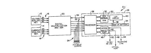
Looking to Fig. 1, a representation of the metering approach of the
10 invention is represented generally at 10. Device 10 is coupled typically to apolyphase line input and employs typical step-down networks as represénted
at blocks 12 and 14 to provide respectively voltage and current related
inputs, for example, for three phases: A, B, and C. In the latter regard, the
phase A-C voltage input signals are provided at three-line grouping 16 while
15 voltage signals corresponding with a current developed by current
transformers are provided at three-line grouping 18. Line groupings 16 and
18 are directed to the sampling input of a high speed digital control stage
represented at block 20. This control stage 20 includes the dual conversion
components for range and data with respect to each sample, as well as
20 multiplication components. The stage further includes a processing network
for treating the parameters derived for each sample and developing pulse
outputs which can be employed for readouts and the like as are
conventionally used in industry. To achieve the speeds required for this
latter processing, a general purpose digital signal processor (DSP) is
25 employed.
Outputs for six selected electrical parameters which always will
include watthours are provided by the latter processing function as
represented by the six-line grouping 22. The pulse carrying outputs at line
grouping 22 are employed in typical fashion to provide I~YZ relay outputs as
30 represented at tapping line grouping 24 and also to provide the inputs to a
microprocessor driven electronic register represented within dashed
boundary 26. Register 26 is controlled from a conventional microprocessor
represented at block 28, the input ports of which are coupled to receive line
grouping 22. In conventional fashion, the microprocessor 28 operates in
35 conjunction with random access memory (RAM) as represented at block 30
as well as in conjunction with a program contained in read only memory
(ROM) as well as electronically erasable read only memory (EEPROM) as
~2~3~4(~0
shown at blocl; 32. The electron;cally erasable read only memory as
represented at block 32 functions to carry calibrating information which is
submitted to the digital signal processor (DSP) function at block 20 at such
time as the device 10 is powered up. This dual directional serial
5 communication is represented by line 34. To maintain the data developed as
outputs at array 22, a back-up battery is employed with the register 26 as
represented at block 36 and line 38. The microprocessor 28 functions to
treat the data received from line grouping 22 and provide a visual display,
preferably through a liquid crsytal (LCD) display represented at block 40.
10 To permit the device 10 to be programmed remotely, a modem as
represented at block 42 is provided which functions to permit carrying out
of programming and communication via a telephone link as represented at
line 44. Similarly, it is desirable to provide for on-site programming, for
example, through an IR communications or optical link. This is provided
15 through a-serial port represented at block 46 and line 48. Also, through the
port 46 as represented at line 50.
To achieve the processing speeds requisite to carrying out a sampling
each degree of a conventional power cycle, for one embodiment of the
invention, a synchronous state machine approach is employed. With such an
20 approach, decisional software overhead and the like commonly encountered
with microcomputers is avoided and a full development of requisite
electrical parameters commencing with watthours is achieved for each
sample degree or about each 46 microseconds. For example, operating at a
S.4 ~IHz clock speed, the synchronous state machine carries out 128 steps to
25 process a 1 sample.
As a prelude to considering the architecture of the circuitry for the
sampling and multiplying technique, reference is made to Figs. 2A-2B where
the operation of the system is illustrated in data flow block diagrammatic
fashion. The figures should be considered in an orientation corresponding
30 with their associative labeling.
Fig. 2A shows that data flow as established for three phases, A-C, and
it may be observed that the components of the îigure are identical and thus
identically labeled. Accordingly, the same numeration is employed to
describe corresponding components îrom phase to phase along with prime
35 notations for phase B and double prime notations for phase C.
Data ~low is shown to commence with the insertion of voltage analog
signals represented at arrow 60 to an analog-to-digital conversion function
--12-
4~90
represented at block 62. These voltage analog signals will be provided for
phases ~-C as well as a zeroing or ground value employed for periodic
adjustment of values of the system. In sirnilar fashion, the corresponding
c~lrrent analog signals are provided as phase designated voltages as
5 represented at arrow 64 shown being directed to an analog-to-digital
function represented at block 66. Preferably, the inputs 60 and 64 are
multiplexed in the sequence phase A-phase C in the noted 1 sampling
intervals for a full cycle of 360. In the order of sampling, first phase A is
sampled, then phase B and then phase C following which a zeroing
10 measurement is taken. Thus, any of the given phase cycles are measured
approximately every third cycle. In the latter regard, 540 are used for
each cycle in order to carry out multiplication to develop such parameters
as var, Q, and volt amps. With the arrangement, the system is capable of
operating in conjunction with single or polyphase inputs, and, in this regard,
15 will be seen to react in conjunction with cross-over events to detect the
commencement of the initial phase under sampling.
The output the A/D function 62 is shown being directed in data flow
fashion to a voltage scaler function as represented at block 72. In effect,
two analog-to-digital conversions are taken with the system, one to provide
20 the scaler data represented at block 72 in which the 12 bits of digital
information representing the amplitude of the 1 sample and a sign bit are
employed to establish 11 scaling levels of amplitude from 0 to peak
amplitude. The initial digital conversion is for this scaling function and, as
represented by flow lines 74, 76 and block 78, this initial value of the
25 amplitude of the sample is used to access a look-up table in random access
memory (RAM) to determine an ll-bit scaling value or factor which is used
as a multiplier. This l l-bit scaler then is provided as represented at lines 80and 82 as an input to a multiplication step represented at circle 84.
The voltage scaler value 72 additionally is used to provide an input to
30 an amplification or treatment stage which amplifies the voltage sample
input 60 prior to a next conversion by analog-to-digital function 62. Thus
the conversion now represented along flow lines 68 and 70 block 86 is one of
voltage data of 11 data bits plus a sign bit. As represented at flow line 88,
these 11 bits then are directed to the multiplication function 84, whereupon
35 a scale adjusted valuation or expanded data digital value is developed of
enhanced significant bits which may have an extent of 21 data bits plus a
sign bit for a highest scale level and this enhanced and highly accurate
-13-
~9~4~0
representation of the amplitude of voltage for the sample degree then is
ava;lable as represented at flow line 90.
The current samples as described at line G4 are converted in similar
fashion as represented at block 66 such that, initially, a scaler current
5 valuation is made, as represented at flow lines 92 and 94 leading to the
scaler function represented at block 96. This current scaler function, as
before, provides an input as represented at lines 74 and 76 to a look-up table
of 11 values in random access memory as represented at block 78. The
resultant scaler or scaling factor, as before, is then provided to a
10 multiplication function as represented at circle 84 and flow lines 80 and 82.llowever, this same scaling value also is utilized to adjust the gain of an
input amplification stage to the conversion function 66 such that a next data
conversion then provides a digital current data signal as represented at
block 98 having 11 data bits plus a sign bit. As before, as represented at
15 line 100,-this current data digital value then is submitted for multiplicqtion
as represented at circle 102 with the RAM contained scaling factor as
represented being asserted from flow line 82. The resultant product, as
represented at flow line 104 will be a highly accurate representation of the
amplitude of the current sample having as many as 21 significant digital bits
20 of information plus a sign bit.
The sampling and digital multiplication function now has highly
enhanced valuations of voltage and current for the given 1 sample.
Returning to flow line 90, the voltage sample is adjusted or corrected for
gain and phase errors. These errors will occur at the front end of the
25 system where analog components such as transformers, scaling resistors, and
conversion functions are carried out. Additionally, phase or time error can
occur in consequence of the transforming as well as conversion. To correct
for these normally encountered vagaries, each meter is tested in the course
of its assembly, for example, in conjunction with a standard. Correction of
30 the output of the meter under test with the standard then is provided by
providing a correction factor for each sample degree of any given cycle and
such data are positioned in random access memory (RAM) at power-up. The
look-up of the correction factor is represented at block 106 and the 21-bit
data output thereof is represented at flow line 108 extending to a
35 multiplication function represented at circle 110. A resultant corrected
voltage sample digital representation which may have as many as 21 data
bits plus a sign bit then is directed as represented by flow lines 112 and 114
~2~
to temporary storage in random access memory as represented at block 116.
The voltage value for the given sample at line 112 is employed to develop a
volthour parameter and thus, the flow line for the value is seen to progress,
as represented by lines 118 and 120 for further treatment. However, as
represented at line 122 and a multiplication function represented by circle
124, a volts2 multiplication may be carried out to provide a volts2 valuation
for processing as represented at flow line 126.
A watt valuation for the 1 sample is provided by a multiplication
represented at circle 128 which provides the product of volts at line 112
with the corresponding current valuation from line 104 as represented at
line 130. This product then is submitted for further processing as
represented by flow line 132.
The parameter, Q, represents a lag in phase of 60 with respect to
watts. Accordingly, a multiplication function is provided as represented at
circle 134 which carries out multiplication of the current digital value as
represented at flow lines 104 and 136 with voltage only after a delay of 60.
Thus, the volt data are withdrawn from RAM memory function 116 as zero
valuation represented at line 138 until after a 60 delay occurs to develop
an output for the Q parameter as represented at flow line 140.
Similarly, the var parameter is one representing at 90 delay. Thus, as
represented by the multiplication function at circle 142, the current values
for the given sample at lines 104 and 144 are multiplied by zero voltage
digital values until after a 90 delay. Accordingly, the voltage digital
valuations are active participants in the multiplication activity represented
at circle 142 only after a 90 delay and the products of the multiplication
extend in the diagram along line 1~3.
A determination of the parameter volt amperes (VA) in essence,
requires an alignment of the voltage and current cycle envelopes. Inasmuch
as the current component may be spaced from the voltage component by as
much as 180, zero crossings are monitored for this function and, as the
zero crossing of the current component is detected, then the voltage values
stored earlier in RAM 116 are engaged in a multiplication function. The
latter function is represented at circle 148 shown accessing the current
valuation from line 104 and RAM contained voltage digital information from
line 150. A resultant VA evaluation for the given sample then is submitted
for further processing as represented at flow line 152.
--15-
~2~
From the above, it may be apparent that, with a maxirmum possible
delay of 180 to develop the V~ output, the total number of sample degrees
for each cycle evaluated will be 540. The resultant outputs of all three
phases ~-C then are seen to be combined at earlier-described lines 120, 126,
132, 140, 143, and 152.
Looking to Fig. 2B, the above designated output flow lines are seen
directed to a data processing function which, as discussed above, is
controlled by a digital signal processor (DSP). However, one further value is
added to the products which are made from the conversion functions 62 and
66. At the conclusion of sampling a full cycle of phases A, B, and C, a zero
valuation is asserted to the conversion function such that any offset values
may be detected for summing correction in the processing procedure.
Looking to the process, it may be observed that the volt digital values for
each degree sample for each of phases ~-C flow as data represented by lines
120 and l54 through a zero correction function represented at block 156.
The resultant corrected valuation, which may be as high as 21 significant
data bits is then submitted as represented at line 158 to an accumulating
register represented at block 160. This register accumulates the values and
provides, in effect, an integrating function which, upon reaching a
20 predetermined value, provides a signal as represented at line 162 which is
directed to an overflow register represented at block 164. Register 164
provides a pulsed output representative of volthours as depicted by flow line
166. Generally, the number of pulses corresponding with a given parameter
valuation is determined by the end user. The data as represented at line 166
25 flows to a parameter selection function represented at block 168 for
outputting as one of six channels of data represented at line grouping 170.
These six channels correspond with line grouping 22 as described in
conjunction with Fig. 1.
In similar fashion, the volt~ parameter data are shown flowing via line
30 126 and, as represented by line 172 and block 174, are corrected for zero
offset, whereupon the data bits which may be as high as 21 are directed to
an accumulating register as represented by line 176 and block 178. As
before, the values accumulate for each phase and, at some predetermined
overflow value, are submitted to an overflow register as represented by line
35 180 and block 182. ~ resultant pulse output is developed from the register
~unction 182 as represented by line 184 representing an integrated valuation
--16--
4~
for volt2hour which then flows to the selection procedure at block 168 for
possible election as an output at line six line grouping 170.
~ata flow representing the electrical parameter, watt, is shown
flowing via line 132 and, as represented at line 186 and block 188, such data
5 are adjusted for zero offset and submitted as represented by data flow line
190 and a selection function represented by switch to either of two
accumulating register functions represented at blocks 192 and 194 via
respective lines 196 and 198. The register function represented at block 192
collects data corresponding with a positive or "watts out" cycle for
10 integration, while a corresponding "watts in" compilation is evolved in
conjunction with the accumulating register function 194. With the instant
digital approach, a determination as to the appropriate polarity for a given
~ampled phase cycle is provided on a historical basis wherein the polarity
then available at a polarity detector function represented at block 200
15 controls the orientation of the selection represented by switch Sl. This
control is represented by dashed line 202. The polarity detector function at
block 200 may be implemented as an up/down counter performing in
conjunction with the earlier-discussed sign bit of the converted data. This
sign bit input to the register is represented by flow line 204 extending from
20 flow line 190. Because of the vagaries of the system and slight phase
deviations which will be encountered during sampling, the polarity detector
will be incremented upwardly with positive sign bit inputs and, conversely,
incremented downwardly with the input of negative bits. However, the
overall history of signage for any given number of samplings, for example
25 360, will determine control over the switching function Sl, i.e. that
indication as to whether the information is with respect to watthours out or
watthours in. As before, the accumulated valuations in register function
192 will be provided as outputs as represented at line 206 for a given
threshold, which information is directed to an overflow register function
30 represented at block 208. A pulse designated output occurs from register
208 as represented by flow line 210 which is directed to the selection
function at block 168 for outputting as a channel at line grouping 170.
Similarly, the watthour in data developed in accumulating register 194 is
outputted, as represented by flow line 212 to an overflow register function
35 represented at block 214 for presentation as pulse data, as represented at
line 216 to the selection function at block 168.
-17-
lZ9q~4~
Q valuations, as represented by the data flow path at line 140, are
shown being corrected for zero offset, as represented by flow line 218 and
block 220, whereupon the data bits for this parameter are subrnitted to a
selection function represented by a switch S2 and lines 224 and 226 to
5 respective accumulating register functions represented at blocks 228 and
230. Block 228 functions to provide an integrated valuation for Qhours out,
while line 230 provides the corresponding valuation for Qhours in. As
before, the general flow of power, as developed by the historic accumulation
of the polarity detector 200 determines the selection represented by
10 switching function S2. Where Qhours out are at hand, then the overflow of
the accumulating register function 228, as represented at line 232 is
directed to an overflow register function represented at block 234. The
resultant, pulse categorized data representing Qhours out are developed and
submitted as represented by line 236 to the selection function represented
15 at block 168 and, if selected, are provided at six line grouping 170.
Correspondingly, the Qhour in integrated valuation evolved at the register
230 provides an overflow output at a predetermined level as represented at
flow line 238 which is directed to an overflow register function represented
at block 240. The resultant pulse designated Qhour in data then are
20 submitted as represented flow line 242 to the selection function represented
at block 168 and thence, if selected, to an output at six line grouping 170.
The flow of var data, as represented at line 143 from the three phases
is shown directed via line 244 to the earlier-described zero offset correction
function represented at block 246. Upon correction, this data flow then is
25 submitted to a dual selection logic to evolve four quadrant varhour
metering. In this regard, as represented by data flow line 248 and sign bit
flow line 250, the signage for each data sample is submitted to a polarity
detector function represented at block 252 which, as before, may be
implemented as an up/down counter. The polar sense of this counter, i.e. +
30 for lag and - for lead will be determined on an historic basis as before, being
an accumulati~n o~, ~or example, 360 sign bit components. Thus, the
valuation representing that history controls a selection function represented
by switch S3, such control being represented by dashed line 254. With the
lag and lead characteristic thus selected by the function represented at S3,
35 the data are then distributed in accordance with overall power flow as
represented by line 256 extending to a selection function represented by
switch S4 leading, in turn, to lines 258 and 260. Selection function S4 is
-18-
controlled, as above, from the polarity detector 200, as represerlted at
dashed line 202 Line 258 extends to an accumulating register 262 which
collects data valuations for varhour lag Ollt and the overflow representing
integrated increments thereof is represented, as presented at line 264, to an
S overflow register function represented at block 266. Pulse categorized
outputs of function 266 are represented by data flow line 268 extending to
the selection function represented at block 168 and, if elected, to six line
grouping 170. An oppositely-disposed power flow selected by the function
represented at switch S4 shows a data flow via line 260 through an
10 accumulating data register function represented at block 270. Thus, for this
direction of power flow, the overflow representing an integrated valuation
of the register function 270 is provided at line 272 extending in data flow
fashion to an overflow register function represented by block 274 and shown
having a pulse categorized data output represented at line 276 corresponding
15 with varhour lead in data.
Where the polarity detection history represented at block 252 shows a
positive valuation or lag condition, then the selection function represented
by switch S3 will elect a data flow represented by path line 278 leading to
the selection function represented by a switch S5. For power flow out
20 conditions, then as represented by line 280 showing data flow to an
accumulating register function represented at block 282, an integration
occurs providing an overflow data flow at line 284 directed to an overflow
register represented at block 286, which, in turn, provides a pulse
categorized output data flow represented at line 288 corresponding with
25 varhour lead out. The latter data are submitted to the selection function at
block 168 and, if selected, will appear at the six line output grouping 170.
Where the selection represented at switch S5 is a power flow to the
utility, then the data flow is represented by line 290 as extending to an
accumulating register represented at block 292 wherein the values of the
30 sampled inputs are collected. The resultant integration provides an
overflow as represented by the data flow line 290 extending to an overflow
register represented at block 296. A pulse categorized output then is
provided, as represented by data flow line 298 corresponding with varhour
lag in data which is directed to the selection function represented at block
35 168 for presentation, if selected, to the six-line grouping 170.
VA data flow is represented at line 152 as flowing as represented by
line 290 to a zero offset correction function represented at block 292. The
--19--
corrected data then flows to an accumulating register function through a
selection feature represented by switch S6 controlled from the polarity
detector 200 via line 202. For a positive history represented at the detector
function at block 200, then the data flow is represented as along line 296
leading, in turn, to the accumulating register represented at block 298. An
integration form of treatment ensues providing an overflow represented at
flow path line 300 directed to an overflow register function represented at
block 302. A resultant pulse categorized signal output representing VA hour
out data then is directed to the selection function represented at block 168
10 for presentation, if selected, to a channel of the six-line output grouping
160.
In the event the power flow is toward the utility, then the data flow
from the selection function represented at switch S6 is along line 306
directed to an accumulating register function represented at block 308 for a
15 value accumulation amounting to an integration. The overflow is then
directed as represented by line 310 to an overflow register function
represented at block 312 to provide a pulse categorized output data flow
represented at line 314 corresponding with the data VA hour in. Flow line
314 is directed to the selection function represented at block 168 and if the
20 subject data are selected, then it will be outputted at one channel of six-line
grouping 170.
Referring to Figs. 3A-3B, the circuit structuring for deriving the
sampling, control including digital multiplication and digital signal
processing (DSP) functions described in conjunction with block 20 in Fig. 1 is
25 revealed. In Fig. 3A, the analog networl<s for treating incoming three-phase
power are represented at blocks 320 and 322. These step down functions
will include conventional voltage and current transformers along with
resistor and capacitive components suited for appropriate scaling and
conversion of current to voltage. The resultant voltage analog signals are
30 presented via three-line grouping 32~ as labeled VA, VB, and VC to
corresponding inputs of a phase multiplexer represented at block 326.
Additionally provided as an input to the multiplexer 326 is a line labeled VZ
representing a zero input for the earlier-described zero offset
measurements.
In similar fashion, the analog current signals for phases A, B and C are
provided at three-line grouping 330 as labeled IA, IB and IC. Additionally, a
line 332 labeled IZ and coupled to ground provides the noted zero offset
-20-
~L29~4C~
input to the multiplexer for zero ofset correction in conjunction with
current.
For the embodiment shown, the requisite speeds or operational rates
for the components shown in Fig. 3~ are derived sampling a synchronous
5 state machine form of control. This control provides in conjunction with a
sampling rate such that the phase A (VA) input is sampled 360 times
followed by the remaining voltage phases and a zero offset measurement at
line 328. Selection of phase at multiplexer 326 is represented at line 334.
Additionally, the current phases are sampled commencing with phase A (IA)
10 and these current inputs are sampled 360 times per cycle. Commencement
of the sampling procedure will be seen to be regulated in conjunction with
the detection of zero cross-overs of the pertinent sinusoids.
Looking momentarily to the counting components of this synchronous
state machine, it may be observed that a state counter is provided at 336,
15 the clock input to which is provided, for example, at 5.4 MHz at line 338.
Reset from line 340 and having a carry output at line 342, the counter 336
provides a 7-bit output at 7-bit bus 344 which functions to sequentially
address an EPROM program memory 346 so as to provide corresponding
sequence of 128 instructions at the 16-bit output data bus 348. Three sets
20 of these 123 instructions will be seen to be employed, one set as a zero cross
routine; one set as a multiply routine and one set as a zero routine. Bus 348
extends, in turn, to a state data expander 350 which functions to provide the
.equisite number of control output lines, for example about 30 required for
exerting control from the synchronous state network. These control outputs
25 are represented at a line grouping represented generally at 352.
The carry output, representing 128 events, having been completed, for
example, for treating a 1 sample, is directed via line 354 to the clock input
of a degree counter 356. Thus, with each clock input, the counter 356 will
provide a progressive count presented at 9-bit output bus 358. Counter 356
30 is reset from lines 340 and 360. Bus 358 transmits the degree count
information to a 90 count or 90 decoder 362, a 60 or 60 count decoder
36~, and a 540 or 540 count decoder 366. The carry out terminal of 540
counter 366, in turn, is directed via line 368 to the clock input of a phase
counter 370. Reset from lines 340 and 372, the phase counter 370 provides
35 outputs corresponding with the completion of a full cycle sampling for each
of phases A, B and C via earlier-described line input 334 to the multiplexer
326. Thus, the multiplexer 326 proceeds through the sequence of phases A,
B and C for both voltage and current in addition to the earlier-noted zero
offset measurement.
The phase d&signated voltage output of phase multiplexer 326 is
provided at line 374 for introduction to the input of a variable gain amplifier
stage 376. Having a gain control represented at line 378 and an output at
line 380, stage 376 provides the ranging input and subsequent scaled data
input at line 380 to the input of a voltage analog-to-digital converter (A/D)
382.
In similar fashion, the sequence of phases A-C for current samples are
provided at line 384 by the phase multiplexer 326 for presentation to the
input of a variable gain amplification stage 386. Gain control to stage 386
.3 represented at line 388 and the output thereof at line 390 is directed to
the input of a current analog-to-digital converter (A/D) 392 Converters
382 and 392, respectively, are controlled from line grouping 352 of the state
l S data expander as represented at lines 394 and 396 so as to perform two
conversions for each degree of amplitude data. This conversion occurs at a
rate adequate to achieve the noted 360 samples per phase cycle.
Accordingly, the converters 382 and 392, which provide 12-bit outputs to a
corresponding 12-bit bus 398 should carry out a conversion within about 5
microseconds. The converters may be provided, for example, as type
AD1572 ADC converters marketed by Analog Devices of Norwood,
Massachusetts. Activation of the converters for the commencement of any
given operation commences with the carrying out of a zero crossing routine
controlled from program memory 346. This 128 step routine i5 outputted at
16-bit bus 348, expanded at expander 350 and presented from line grouping
352 as controls to converters 382 and 392 via respective lines 394 and 396.
Thus sampling occurs during this routine specifically with respect to the
voltage inputs for phase A, conversions thereof at zero gain input from lines
378 being presented to 12-bit bus 398. Bus 398, in turn, extends to a zero
cross-over detector network 400 which responds to the noted sign bits
output of converter 382 to detect a change of polarity and thus a zero cross-
over for any given sinusoid. Detector 400 is enabled for this search from
line 399 extending from State Data Expander 350. When this cross-over for
voltage is detected, an output is provided at lines 402 and 404 which is
directed, inter alia, to the program memory 346 to cause it to enter into a
multiply routine which is another 128 steps in extent. At the
commencement of this multiply routine, a range latch 406 is controlled via
4~
iine grouping 352 of the synchronous state machine as represented at line
408 to provide a zero gain output control via lines 378 and 388 to respective
gain stages 376 and 386. Stage 376 then provides a sample ~nput for the
first degree of sampling at line 380 which is converted by converter 382 to a
12-bit range digital value at bus 398 representing 11 bits of range data plus
a sign bit. This information is provided simultaneously to the range latch
406 via bus 398 as well as to a range address latch 408. Latch 408 is
controlled by the synchronous state machine from line grouping 352 as at
line 410.
Responding to the range data presented from bus 398, range latch 406
then adjusts the voltage gain at amplification stage 376 in accordance
therewith. Thus, where the ranging value is higher, the gain is
correspondingly set lower. Generally, eleven values of gain are provided
representing eleven amplitude scaling regions. Voltage converter 382 then
provides a data conversion which is presented at bus 398 and to a bus driver
which directs the 11 bits of data digital values and sign bit to a bus driver
412. Controlled under the multiply routine from program memory 346 via
line grouping 352 and specifically line 414, the bus driver responds at an
~ppropriate time to present the 12 bits of data digital value data to 12 of
the 24 bits of bus 416. 24-bit bus 416 extends to a 24 x 24 bit multiplier
418. Controlled by the synchronous state machine from output line grouping
352 and specifically as represented at line 420, the multiplier 418 preferaby
is a high speed, low power 24 x 24-bit parallel multiplier fabricated in 1.5
micron CMOS and marketed as a type ADSP-1024A by Analog Devices,
Norwood, Massachusetts. The ranging data as presented to range address
latch 408 are employed via 8-bit bus 422 to address a random access
memory (RAM) 424 to find one of 11 scaling factors corresponding with the
range data procured from converter 382. Upon being accessed from
memory, this scale multiplier then is submitted via 24-bit bus 416 to the
multiplier 418 for multiplication with the second conversion data digital
values. The resultant accurate evaluation of voltage expanded data for the
1 sample at hand is returned via bus 416 to memory 424 for temporary
storage.
Very shortly (1 microsecond) following the sampling of data for 1 of
voltage at line 374, current is sampled from line 384, being directed through
variable gain amplifier 386 at a zero level of gain to be presented via line
,90 to converter 392 to provide a range conversion. As before, this range
--23--
~2~3~4~
digital value, present as 12 bits including one sign bit is submitted both to
the range latch 406 and to the range address latch 408. At range latch 406,
the data are employed to select an appropriate gain value of 11 levels for
adjusting the gain at variable gain amplifier 386. With lower amplitudes,
S higher gain values are asserted. ~ next conversion by this amplified value
at line 390 then is undertaken by converter 392 and presented at bus 39d as
12 bits of data digital values including a sign bit and is directed to bus driver
412, whereupon it is presented to multiplier 418 via 24-bit bus 416.
Correspondingly, the range information supplied to the range address latch
408 is submitted via 8-bit bus 422 to a look-up table in RAM memory 424 to
provide an appropriate multiplier or scaling factor corresponding with the
scale level determination for submittal to multiplier 418. The resultant
product for the 1 current sample will have as many as 21 significant bits
plus a sign bit.
Thus with very accurate digital representations for a sampled 1 of
voltage and the corresponding sampled 1 of current of the phase A cycle
detected, the synchronous state machine then proceeds to carry out
necessary multiplications. As a first aspect of this procedure, the accurate
voltage data now retained in RAM 424 are submitted via bus 416, bus driver
426 (Fig. 3B) and 24-bit bus component 428 to the data input of a digital
signal processor (DSP) 430. During this interval of time, the 24-bit bus at
416 is under the control of the synchronous-state machine and thus, the DSP
430 is caused to respond to the asserted data via a data ready signal from
the synchronous state machine developed from line grouping 352 and
specifically shown presented via line 432. Processor 430 may, for example,
be provided as a type TMS 32010 Digital Signal Processor which is a 16/32-
bit single-chip microcomputer combining the flexibility of a high speed
controller with the numerical capability of an array processor. The device
offers an alternative to multi-chip bit/processors and is marketed by Texas
Instruments, Inc., Houston, Texas. Device 430 functions with the
synchronous state machine to provide the earlier-described 5.4 MHz clock
output at line 338 and performs in conjunction with a program retained in a
programmable read only memory (EPROM) 434. Device 434 carries the
program control for DSP 430 and is shown coupled with 24-bit bus 428 as
well as with a 16-bit address bus 436 in common with DSP 430. To provide
further control, the 16-bit bus 436 is shown extending at 438 to a control
expander 440 to provide a control input via line 442 to memory 434. Line
--2~--
4~)
444 is the DSP 430 control to expander 440. Control additionally i9 asserted
via line 446 to a bus driver 448 representing an interface with 8-bit bus 422.
Line 450 is shown extending to control the bus driver 426, while adjacent
line 452 represents a control input to RAM memory 424 thorugh OR gate
454 and line 456 to provide control thereover during those minor portions of
the cycle wherein the DSP 430 has control over the major bus structure.
During such control, for example at power up, DSP 430 functions to convey
the earlier described data used for retaining magnitude/phase correction
values developed during calibration to RAM 424 from processor 28 (Fig. 1).
The opposite input to gate 454 emanates from line 458 representing a
control from the line grouping 352 of the synchronous state machine.
Finally, a control represented by line 460 extends from the control expander
440 to an output latching function represented at 462. This latching
function 462 is coupled with 24-bit bus 428 and functions to develop the six
channels of selected output described in conjunction with Fig. 1 at 22 and
represented herein by the same numeration. Serial communication between
the electronic register 26 shown in Fig. 1 at line 34 is represented with the
same general numeration in Fig. 3B at lines 464-466. Lines 464-466 carry,
respectively, reset data, received serial data and transmitted serial data.
Returning to Fig. 3A, following the submission of voltage values as
multiplied by the gain and phase correction value, the corrected voltage
value is retained in RAM 424 and a DATA READY signal is submitted via
line 432 to DSP 430 for submittal of that information thereto. The
synchronous state machine then recalls the corrected voltage data from
RAM 424 and again submits it twice to the multiplier 418 for developing a
voltage2 value. Again, the DATA READY signal is provided as represented
at line 432 to DSP 430 for submitting the voltage data thereto.
The voltage data again are read from RAM 424 and are multiplied by
the then-available current data to provide a watt valuation for the sampled
degree. Accordingly, a DATA READY signal again is provided at line 432 to
DSP 430 such that it might receive this information. The address to RAM
424 for submitting the corrected voltage data to multiplication in
developing this watt value is developed from a watt degree counter 468
having an output coupled with bus 422 leading, in turn, to RAM 424. Watt
degree counter 468 develops a succession of 360 addresses to RAM 424 in
correspondence with a clocl~ input thereto for each degree developed at line
342 and e~tending to the counter via line 470. Simultaneously with the
-25-
commencement of the first address from the counter 468 to RAM 424, a 360
degree decoder function represented at block 472 is activated from line 473
of grouping 352 for a watt monitoring function under control from bus 422.
At the termination of 360 degrees of watt evaluation, the watt degree
counter 468 will be reset from decoder function 472 as represented at line
474. Clock enablement to the watt de~ree counter 468 is provided from line
grouping 352 and specifically represented at line 476, while output
enablement of the address devised by the counter 468 is provided from the
same line grouping as represented at line 478. Line 476 extends from line
10 402 and the voltage zero crossing from zero cross detector 400. Thus, the
watt degree counter is initially activated from this zero crossing.
The determination of Q valuations for each sample is determined with
respect to a delay representing a phase difference of 60. Accordingly, Q
determinations are not made until 60 samples have been developed. To
15 provide this feature, a Q degree counter 480 is provided which, for 60
samples, provides an address output at bus 422 serving to assert a zero
voltage valuation from RAM 424 to the multiplication function 418. Thus,
for those first 60 samples, the Q valuation will be zero. However, upon the
60th sample, the Q counter then functions to submit the corrected voltage
20 valuations from the single degree sampling in sequence by addressing RAM
424. These values then are multiplied at multiplier 418 by the then
instantaneous valuation for current to provide a Q valuation. At the
commencement of counting following the 60 lag, 360 decoder 412
ccommences to count through 360 and to provide a reset to the Q degree
25 counter 480 as represented at line 482 to determine the end of a Q
evaluation. Counter 480 is enabled from the line grouping 352 as
specifically represented at line 484 by assertion of a clock enable signal
thereto and its output is enabled as above discussed from the earlier-
described 60 decoder 364 via line 486. One degree clocking to the counter
30 480 is provided from earlier-described line 342 through line 488.
Var valuations are characterized by a 90 phase variation. Thus, a var
degree counter 490 is provided which functions to address the RAM 424 via
bus 422 to output a zero voltage value for the first 90 samples or 90. A
determination of the 90th degree is provided by the earlier-described 90
35 degree decoder 362 and the information corresponding thereto is provided at
line 492 for assertion at the clock enable input of counter 490. The output
enable for counter 490 is provided from line grouping 352 as represented at
--26 -
~2~
line 494 while the clock input thereto derives from earlier-described line
342 and line 496. As before, counter 490 further is monitored by the 360
decoder function 472 such that upon the 91st sample or degree, 360 samples
are decoded following which the counter 490 is reset by an input from
decoder 472 as represented at line 496.
As noted earlier, the development of a volt ampere (~A) quantity
requires, in effect, a coincidence of the envelopes of the voltage and
current sinusoids for a given cycle. Accordingly, a VA degree counter is
provided at 498 which is activated at its clock enable input by a zero
crossing of the current signal as detected by detector 400 and asserted to
the counter from line 500. Counter 498 is clocked from earlier-described
line 342 and its output is enabled frorr~ the synchronous state machine line
grouping 352 as specifically represented at line 502. The counter 498 is
monitored by the 360 degree decoder function 472 such that it is reset
following 360 degrees of counting and addressing memory 424 via line 504.
All of the above determinations are made throughout a span of 540 degrees
or 540 clock counts. Accordingly, at the termination of devising volts,
volt2, watt, Q, var and VA values, the 540 degree decoder 366 provides a
clock input to phase counter 370 via line 368. Counter 370 then provides an
output via lines 334 to phase multiplexer 326 to commence with the
evaluation of phase B of the input. Control with respect to recommencing a
search for a zero crossing of the voltage B phase is provided to function 400
as represented at line 506 and earlier-noted enablement line 399.
Following an initial zero cross routine, the synchronous state machine
essentially repeats the above detailed procedure through each of the phases
A, B and C of the input. It then enters a zero or offset determining routine
wherein the sample inputs essentially are brought to a zero value and
introduced to the phase multiplexer 326 as applied from lines 328 and 332.
~nder the control of the synchronous state machine via line grouping 352,
the device carries out an initial ranging input for voltage and current
through respective amplifiers 376 and 386 ~ollowing which, range
ineormation is supplied to the latch 406 as well as to the address latch 408.
Latch 406 then adjusts the gains of amplifiers 376 and 386 in accordance
with the evaluated range and data sampling then takes place for the first of
360 samples. The range codes in RAM 424 then are multiplied with the data
to provide an enhanced voltage current evaluation and, for each of the 360
sarnples, the DSP 430 is interrupted by a DATA READY signal at line 432
-27-
such that zero interrupt data may be provided. These data are stored in on-
board random access memory. At the termination of this zero routine on
the part of the synchronous state machine, then an end of program signal is
developed at line 508 extending from line grouping 352 of the state data
e~cpander 350. Line 508 is seen to extend to earlier-described line 340 which
functions to reset the counters 336, 356 and 370 as well as to provide an end
o~ program input pulse to the DSP 430. The synchronous state machine then
enters the noted zero cross routine for commencing a ne~t three phase and
offset or zero setting evaluation.
Referring to Figs. 4A-4C, a program flow chart for the synchronous
state machine components as discussed in conjunction with Fig. 3A is set
forth. This program also may be employed to operate a high speed general
purpose digital signal processor as an alternative to the sychronous state
machine aproach described above.
In general, the synchronous state components as described in
conjunction with Fig. 3A operate in relative independence from the DSP 430
driven processing described in conjunction with Fig. 3B. A communication
between these two functions occurs when the synchronous state machine
indicates a OATA READY condition as described in Fig. 3A in conjunction
20 with line 432. The DSP 430 functions to load calibration constants into
RAM 424, whereupon the synchronous state machine is permitted to
perform. At such time, the synchronous state machine is stopped so that
the DSP 430 can take control of the data bus components 426-428.
Fig. 4A shows a zero cross routine region represented by vertical line
25 520. This initial portion of the routine is shown commencing at line 522
leading to the instructions represented at block 524. At this position, the
synchronous state machine waits for a stop command of the DSP 430. In the
event such a stop occurs for calibration constant loading into RAM 424, then
at some point dictated by the DSP 430, the instant program recommences,
30 as represented at line 526 and block 528 to carry out voltage conversion, as
described in conjunction with phase A and analog-to-digital converter 382.
rhis voltage conversion continues until such time as the zero cross detector
network 400 detects a voltage phase A zero cross-over. Thus, the program
proceeds as represented at line 530 and block 532 to provide the query as to
35 whether a volt zero crossing has occurred. If it has not, then as represented by loop line 534, the progam waits until such volt zero crossing has
occurred. Where such crossing does occur as detected by the detector
-28-
~2~4~
network 400, then as represented at line 536 the zero cross routine is exited
and a multiply routine commences. The extent of this multiply routine is
represented in the figures by vertical line 538.
Line 536 is seen to lead to the instructions at block 540. At this
position, the volt and current range conversion is carried out by respective
converters 382 and 392 to determine the scaling or range digital values as 12
bit outputs, including a sign bit. Accordingly, as repesented at line 542 and
block 544, these range values are stored, for example, in range latch 406 and
range address latch '108. From range latch 408, scaling factors are
addressed and accessed from RAM 424. Upon completing such storage, as
represented at line 546 and block 548, the A/D converters are ranged by
applying appropriate amplification gain input to amplifers 376 and 386.
Upon completion of ranging, as represented at line 550 and block 552, volt
and current data conversions are carried out to provide 12 bits of data from
each converter, the latter incorporating a sign bit. Following the conversion
of volt and current data, as represented by line 554 and block 556, the range
code or scaling factor is multiplied by the subsequently obtained amplitude
(digital) values to derive an accurate, expanded voltage data valuation for
the degree being sampled, which, for example, may have an extent as high
as 21 significant bits. Then, as represented by line 558 and block S60 the
r~sultant voltage data are multiplied by a gain and phase correction value
again at the multiplier 418. Such values were inserted as calibration
constants in RAM 424~ The program then proceeds as represented at line
562 and block 564, the gain and phase correction voltage data are stored in
RAM 424 and DSP 430 is interrupted with a DATA READY signal as
described at line 432. Volt data then are made available for processing by
DSP 430 in the manner thus far described in connection with Fig. 2B.
Following such volt data submission, as represented at line 566 and block
568 the corrected volt data are withdrawn from RAM 424 and multiplied in
squaring fashion at multiplier 418 to derive volt2 data. Such data are
submitted to the DSP 430 in conjunction with a DATA READY signal as
provided from line 432. Thus, at this juncture, the DSP 430 is carrying out
development of volthour data and volt2hour data. As represented at line
570 and block 572, the current range code is drawn from RAM 424 and
multiplied with the second data conversion for current as provided from
converter 392 to develop expanded current value data of high accuracy
having a possible extent of 21 bits. Line 574 then shows the program leading
-29-
~2~
to instructions for reading volt data from RAM 424 and multiplying it by the
noted current data to provide watt data as shown at block 576. These watt
data then are submitted to the DSP 430 in conjunction with a DATA READY
signal from line 432. Line 578 shows the multiply routine then leading to
5 the instructions of block 580 providing for the reading of volt data and
multiplying it by current data under the conditions asserted by the var
degree counter 490, providing for a 90 degrees or sample step delay. At the
conclusion of the determination of var data, the DSP 430 is interrupted with
a DATA READY signal from line 432 and the var data are read into it for
10 the instant one degree sample. Line 582 shows the multiply routine
continuing to the instructions at block 584 for developing Q data as a
multiplication of current data by volt data delayed by 60 degrees or
sampling steps to achieve a Q data valuation. These Q data are read into
DSP 430 in conjunction with a DATA READY signal 432 and the multiply
15 routine continues as represented at line 586. Line 586 leads to the
instructions at block 588 providing for the reading of volt data and
multiplying it by current data which, as described above, are developed only
following the detection of a current zero cross-over by network 400. Upon
completion of the multiplication, DSP 430 is provided these VA data in
20 conjunction with a DATA READY signal at line 432 and the program
continues as represented at line 590. Line 590 leads to a query as to
whether 540 degrees have been sampled as represented at block 592. In the
event of a negative determination, then the given phase of phases A, B or C
has not been fully sarnpled 540 times and, as represented by loop line 594
25 the program returns to line 536 to await completion of the computation of
all electrical parameters for a given phase ~ull cycle of 360.
In the event the determination of the inquiry at block 592 is in the
affirmative, then as represented at line 596 and block 598, a determination
is made as to whether three phases, A, B, and C have been evaluated to the
30 extent of a full 540 cycle each. If that is not the case, then as represented
by loop line 600 the program returns to line 522 (Fig. 4A) to again carry out
the zero cross and multiply routines.
Where the inquiry at block 598 is in the affirmative, then as
represented at line 602, the program enters the zero routine within the flow
35 diagram region represented by vertical line 604. Line 602 leads to the
instructions at block 606 wherein a watchdog synchronizing register is set.
DSP 430 responds to this register to effect a synchronization by self-
-30--
adjustment and the zero routine continues as represented at line 608 and
block 610. Generally, the zero routine repeats the procedural steps which
are carried out in performing a watt calculation. In this regard, block 610
shows that voltage and current range conversions are carried out at
respective analog-to-digital converters 382 and 392. Thus, the scaling range
data are obtained and, as represented at line 612 and block 614 the range
codes are stored, following which, as represented at line 616 and block 618,
the a-to-d converters 382 and 392 are appropriately ranged in consonance
with the determined range codes by appropriate gain adjustments of
10 respective amplifiers 376 and 386. Voltage and current data conversion then
are carried out as represented at line 620 and block 622, whereupon, as
represented at line 624 and block 626 the range code or scaling factors
accessed from RAM 424 are multiplied by the data to achieve an accurate
representation for the zeroing determination, which may have as rnany as 21
15 bits of voltage data. Similarly, as represented at line 628 and block 630 thesame multiplication approach is carried out with respect to current data.
The zero routine then continues as represented at line 632 and block 634 to
provide for the multiplication of volt data by current data, following which
the DSP 430 is interrupted with a DATA READY signal at line 432 to
20 provide for storage of the zero offset data. As these data are stored, as
represented at line 636, block 638 and line 640 an end-of-program
enabiement signal is passed to DSP 430 via lines 508 and 340. It may be
recalled in conjunction with Fig. 3A that this signal also functions to reset
the state counter 336, the degree counter 356, and the phase counter 370.
25 The synchronous static machine then continues to repeat the program as
represented by line 640 extending to line 522 (Fig. 4A).
Looking to Figs. 5A-SG, a flow chart is revealed representing the
program for the digital signal processor 430 as retained in memory 434.
These figures should be considered in a mutual vertical orientation in the
30 order of their alphabetical suffixes. As represented by the vertical region
lines 6S0-653, the instant program is comprised of four component parts, a
communications routine at 650, a read zero data routine at 651, a read six
measured quantity data routine 652, and a process measured quantities and
outputs routine 653.
Fig. 5A shows entry of the program with the communications routine
650 as commencing with a reset input from the electronic register 26 (Fig.
1) as asserted as described in Fig. 3B at line 464~ This reset is shown
-31--
entering the program at line 656 and is seen to function to provide a stop
synchronous state machine instruction at block 658. The latter command
shows a position in program where the synchronous state machine can be
halted such that control of the bus components falls under DSP 430. This
stop command corresponds with the wait for stop instruction at block 524 in
Fig. 4A. Control of the bus components is established by the DSP 430, then
as represented at line 660 and block 662, serial communication is established
with the processor register 26 (Fig. 1) and magnitude and phase correction
values are loaded by DSP 430 into the RAM 424 of the synchronous-state
10 machine. It may be recalled that these correctional data are maintained in
the register 26 on a non-volatile basis due to the use of an EPROM 32.
Following the loading of requisite constants into RAM 424, as
represented at line 664 and block 666, the synchronous state machine is
released and, as set forth in Fig. 4A at block 528, voltage conversion
15 activities ensue and the synchronous state machine proceeds to block 606 at
the commencement of its zero routine to set a watchdog synchronizing
register. The DSP 430 awaits this position in the program as represented at
line 668 and block 670 wherein a query is made as to whether the watchdog
synchronous register has been set. In the event it has not been set, then as
20 represented at loop line 672, the instant program awaits such activity prior
to entering a read zero data routine. By so operating the synchronous state
machine and ignoring the output, the machine in effect is cleared of
spurious data and the like to assure accuracy at such time as viable readings
commence to be taken.
~Vhen the watchdog register is set as represented at block 606 in Fig.
4C, the synchronous state machine program commences its zero routine
represented at vertical line 604 while, simultaneously, the instant program
commences to read the outputs of that routine. Thus, with an affirmative
determination at block 670, as represented at line 672 and block 674, the
30 program enables its interrupt Eor purposes of processing zero data as
available and, in the meantime, as represented at line 676 and block 678 any
output routines are serviced. However, when zero data are ready, ~he DSP
430 is interrupted with a DATA READ~ input as described in connection
with line 432. Such an interrupt is shown at line G80 leading to block 682
35 providing for the reading of zero data as provided in conjunction with block
634 (Fig. 4C). Upon reading such zero data, as represented at line 684 and
block 686, the interrupt register is set and, as represented at line 688, the
--32--
interrupt routine returns. Prior to the interrupt, the service output routine
as represented at block 678 continues as represented at line 690 and block
692 until such time as the above-discussed interrupt register i9 set. Until
such time, as represented at line 694, the service routine loops awaiting the
5 interrupt. Following the setting of the interrupt register, as represented at
line 696 and block 698, the program changes the interrupt vector as it enters
the read six measured quantity data routine. During this routine, the data
comprised of volts, volts2, watt, Q, var and volt amperes (VA) are read by
DSP 430. Accordingly, as each of these interrupts occurs as described at
10 blocks 564, 568, 576, 580, 584 and 588 in Figs. ~A-4B, the measured quantity
of data is read as represented at lines 700 and 702 leading to block 704
describing the reading of measured quantity data followed, as represented at
line 706 and block 708 by the incrementing of the interrupt counter.
Following such incrementation, as represented at line 710 and block 712, the
15 interrupt is enabled and the routine returns as represented at line 714. Line700 is shown leading to block 716 which functions to determine whether or
not six interrupts have been received, in the event they have not, then as
represented at loop line 718, the program dwells until such sixth interrupt
occurs. Upon the occurrence of the sixth interrupt, as represented at line
20 720 and block 722 the program enters the processing of measured quantity
output routine having now completed the reading of computed quantities.
Looking momentarily to Fig. 6, a time representation of the activities
of the synchronous state machine (SSM) with respect to the digital signal
processor (DSP) ~30 is represented. Where sampling a 60 Hz signal, each
25 degree or sample will persist for 46.3 microseconds as labelled above time
line 724 in the figure. ~bove line 72~ as labelled "SSM", as an example, a
sequence of degrees, ranging from degree 9 through degree 12 are depicted.
It may be observed that about one-half of the elapsed time of the sample
degree interval will be taken up with the earlier-described sampling
30 procedures as labelled "S". The remaining portion of the given degree
interval will be involved with the earlier-described multiplication
procedures of the SSM 430. DSP 430 commences the above-described
reading procedure as represented at vertical line region 652 for about a
period of time corresponding with the multiplication procedures of the same
35 degree under analysis as labelled "RD". There then ensues the instant
processing routine for the remainder of that sampled degree.
-33-
)4C~
Returning to Fig. SB, block 722 shows that the processing procedure
carried out by DSP 430 commences with the adding of zero data to watt
data following which, as represented at line 726 and block 728, a
determination is made as to whether the sign bit of the watt valuation is 1
or 0. In the event that it is a 1, then as represented at line 730 and block
732 a watt polarity register is incremented and the program continues as
represented at line 734. On the other hand, in the event the sign bit
determination at block 728 shows a zero value, then as represented at line
736 and block 738 a decrementation of the watt polarity register is made
and the program continues as represented at line 734. Generally, three
register functions will be seen to be involved in the program, one serving to
evolve the history of polarity as described in conjunction with blocks 732
and 738; register function accumulating data values, one for plus and one for
minus in that regard; and a third register function that provides the earlier-
described pulse forming overflow accounting.
Line 734 is seen extending to the input of block 740 wherein a query is
made as to whether the watt polarity register is less than zero. In effect,
this register is an up/down counter such that incremented or decremented it
moves about a neutral zero value in either a positive or negative direction.
A positive direction is one considered to be a history of 360 samples
indicating that the power flow is "out" in the accepted commercial sense,
while a corresponding history representing a negative valuation is considered
a power flow in the llinll convention. Thus, where the query at block 740
shows that the polarity is not less than zero, then as represented at line 742
and block 744 the watt data are added to the watthour out output register
and the program proceeds as represented at line 746. On the other hand, an
affirmative response to the query at block 740 provides, as represented at
line 748 and block 750, that the watt data are added to the watthour in
output register and the program proceeds as represented at line 746. Line
746 then is seen leading to block 752 representing a servicing of the
watthour out output routine for developing the earlier-noted pulsed output
quantities. This is carried out by adding the data to an output register and,
when that compiled data are above a predetermined threshold, pulses are
outputted corresponding with watthours. The routine then proceeds as
represented at line 752 and block 756 to determine whether or not the
watthour in output function has been enabled. Such enablement will be at
the election of the user, a total of si~ output channels being elected with
-34-
o~
the instant circuit architecture. In the event watthours have been enabled,
then as represented at line 758 and block 760 the watthour in output routine
is serviced as described in conjunction with watthour out at block 7S2. The
routine then proceeds as represented at line 762. In the event of a negative
determination at block 756, then as represented at line 764, this servicing is
ignored and the routine progresses to the inquiry at block 766 for a
determination as to whether the Qhour out feature has been enabled. In the
event that it has, then as represented at line 768 and block 770, the zero
ofset data is added to the Q data and, as represented at line 772 and block
774 a determination is made as to whether the watt polarity register is less
than zero. As before, this provides a historical determination as to the
direction of power flow. In the event the determination at block 774 shows
the polarity to be less than zero, then as represented at line 776 and bloch
778, the Q data are added to the Qhour out output register and the program
proceeds as at line 780. On the other hand, where the inquiry at block 774
indicates that the polarity is greater than zero, then as represented at line
782 and block 784, the Q data are added to the Q hour in output register and
the routine proceeds as at line 780 to the instructions at block 786. These
instructions provide for the servicing of the Qhour out output routine in the
20 manner described in conjunction with block 752 above. The routine then
continues as represented at line 788 to the inquiry at block 790 wherein a
determination is made as to whether the Qhour in feature has been enabled
at the behest of the user. In the event that it has, then as represented at
line 792 and block 794 the Qhour in output routine is serviced as above-
25 described and the program proceeds as at line 796. In the event the
determination at line 790 is in the negative, then as represented at line 798
the routine proceeds to the inquiry at block 800.
Returning to the inquiry at block 766, in the event the Qhour out
feature of the system is not elected by the user, then as represented at line
30 802 the routine skips to the input to the instantly considered inquiry at block
800 determining whether or not a varhour lag out feature has been enabled
in conjunction with election by the user. ln the event that it has, then as
represented at line 804 and block 806 zero offset correction data are added
to the var data and the routine continues as represented at line 808 to the
35 inquiry at block 810. Thus, four quadrant varhour metering procedures are
undertaken. In this regard, the inquiry at block 810 determines whether the
var sign bit is a 1 or a 0. In the event it is a 1, then as represented at line
-35--
04C~
812 and block 814, the var polarity register is incremented and the program
proceeds as represented at line 816~ On the other hand, where the var sign
bit is a zero, then as represented at line 818 and block 820, thc var polarity
register is decremented and the program proceeds ia line 816 to the inquiry
represented at block 822. At blocl< 822, a determination is made as to
whether the var polarity register is valued below zero. In the event that it
is not, then as represented at line 824 and block 826, power îlow is
determined with respect to the condition of the watt polarity register.
Where that condition is less than zero, then as represented at line 828 and
block 830, the var data are added to the varhour lag out output register and
the routine continues as represented at line 832. Where the determination
at block 826 is in the affirmative, then as represented at line 834 and block
836, the var data are added to the varhour lead in output register and the
routine continues as at line 832. Returning to block 822, where the var
polarity register is less than zero, then as represented at line 838 and block
840, a determination is made again as to whether the watt polarity register
is less than zero. In the event of a negative determination, as represented
at line 842 and block 844, the var data are added to the varhour lead out
output register and the routine continues as at line 832. On the other hand,
where the determination at block 840 shows an affirmative determination,
then as represented at line 846 and block 848, the var data are added to the
varhour lag in output register and the routine continues as at line 832. Line
832 is seen then leading to block 850 representing a servicing of the varhour
lag out output routine, that parameter having been determined to be enabled
earlier in conjunction with block 800. As before, this servicing involves the
determination as to whether quantity numerical values have reached a
threshold value in register so as to evolve a pulse output representing at
time based integration. The routine then continues as represented at line
852 and block 854 to a determination as to whether varhour lead out has
been enabled. In the event that it has, then as indicated at line 856 and
block 858, the varhour lead out output routine is serviced in the manner
described in conjunction with block 850. The routine then continues as
represented at line 860. In the event the determination at block 854 is in
the negative, then as represented by line 862 the program continues to the
determination at block 864. At the latter block, a determination is made as
to whether the varhour lag in feature has been enabled in consonance with
the desires of the user. In the event that it has, then as represented at line
866 and block 868, the varhour lag in output routine is serviced as described
in the above service procedures. The routine then proceeds as represented
at line 870. Where the determination at block 86~ is in the negative, then as
represented by line 872, the routine continues to the determination at block
87~ querying whether the varhour lead in feature has been enabled in
consequence Oe the user requirement. Where that is the case, then as
represented at line 876 and block 888, the varhour lead in output routine is
serviced to provide a pulse categori~ed data output and the routine
continues as at line 890. Where the determination at block 874 is in the
10 negative, then as represented at line 892, the routine continues without
servicing procedures. Returning to Fig. 5D, where the determination at
block 800 that varhour lag out features have not been enabled, then it is the
design of the program that the user will not have requested further var data.
Accordingly, as represented at line 894, the routine jumps to line 890 and
lS the next inquiry at block 896 wherein a determination as to whether VAhour
out has been enabled is made. Where that is the case, then as represented
at line 898 and block 900, the zero offset data are added to VA data and the
routine continues as represented by line 902 to the inquiry represented at
block 904. At this position, a determination is made as to whether the watt
20 polarity register is less than zero. In the event it is not, then as represented
at line 906 and block 908, the VA data are added to the VAhour out output
register and the routine proceeds as indicated at line 910. On the other
hand, where the watt polarity register indicates a value less than zero
representing a power flow towards the utility, then as represented at line
25 912 and block 914, the VA data are added to the VAhour in output register
and the routine proceeds as at line 910 to the instructions at block 916
providing for the servicing of the V~hour output routine in the above-
discussed manner wherein values are added to a cumulative register and the
overflow above a given threshold therein is employed to produce a pulse
30 categorized output.
The routine then proceeds as represented at line 918 to the inquiry at
block 920 wherein a determination is made as to whether the VAhour in
output category has been elected by the user. In the event that it has, then
as represented at line 922 and block 924, the VAhour in output routine is
35 serviced in the manner above-discussed and the routine continues as at line
926. Where the determination is in the negative at block 920, then as
~:~9~)4~
represented at block 928, the routine continues to a determination as
represented at block 930 concerning volthours.
Returning momentarily to Fig. SE, it may be observed that where the
determination at block 896 has been made that the VAhour out parameter
5 has not been enabled, then as represented at line 932 the routine skips to the volthour determination routine commencing with block 930 querying as to
whether volthour parameters have been elected by the user as by
enablement in the program. Where that is the case, then as represented at
line 934 and block 936, the volt data are added to the volthour output
10 register and, as represented at line 938 and block 940 the volthour output
routine is serviced to generate a pulse categorized output signal and the
routine continues as at line 942.
Where the determination at block 930 is in the negative, then the
routine jumps as represented by line 944 to line 942 and the query at block
15 946 determining whether the volt2hour parameter has been enabled in
accordance with user desire. Where it has, then as represented at line 948
and block 950 the volt2 data are added to the volt2hour output register and,
as represented at line 954 and block 955 the volt2hour output routine is
serviced to generate a pulse categorized output for the register 26. The
20 routine then continues as represented at line 956. Where the determination
at block 946 is in the negative, then as represented at line 958, the program
path, in turn, loops as represer1ted at line 956 to the inquiry at block 960
shown in Fig. 5A determining whether or not the watchdog synchronous
register has been set. In the event that it has not, then, as represented at
25 line 962, the DSP program continues with the reading of six more measured
quantities of data and proceeds to process such data. On the other hand,
where the watchdog synchronizing register has been set, then as represented
at line 96 ~, the program returns to change the interrupt vector as
represented at block 965. The program then returns to enable the interrupt
30 as represented by line 967 leading to block 674 and continues as above-
described.
The implementation of the programs described in conjunction with
Figs. 5 and 6 can be provided with other computational or processing devices
than those heretofore described. For example, as more advanced general
35 purpose digital signal processors become available, they can be substituted,
particularly for the synchronous state machine heretofore described. One
such device identified as a 56-bit general purpose DSP marketed under
--38-
~.2~ 0
Model No. DSP56001 by Motorola, Inc. features 512 words of full speed on-
chip program RAM memory, to preprogram data ROMs and special on-chip
bootstrap hardware to permit convenient loading of user programs into the
program RAM. A co-feature of the device is to provide for 10.25 million
5 instructions per second (MIPS). Looking to Fig. 7, the implementation of
such device is portrayed in general at 970 in block schematic form. One
such DSP device which substitutes for the synchronous state machine earlier
described is represented at block 972. The DSP 972 receives the 11 bits of
data and a sign bit along bus 974 an provides control outputs as represented
10 in general at line grouping 976. One such control is represented as lines 978and 980 extending as controls to a voltage phase multiplexer 982 and a
current phase multiplexer 984. Note that voltage analog inputs for phases
A, B and C as well as a zeroing input, Z, are introduced via line grouping 986
to multiplexer 982, while, correspondingly, scaled current analog inputs for
15 phases A, B and C along with a zero input, Z, are provided from along line
grouping 988 to multiplexer 984.
Phase control is provided to the multiplexers 982 and 984 via
respective lines 980 and 978 and the analog signals are presented therefrom
via respective lines 990 and 992 to respective variable gain amplification
20 stages 994 and 996. As before, an initial ranging unity gain setting is
provided at amplifiers 994 and 996 via controls represented at respective
lines 998 and 1000 emanating from line grouping 976. The initial ranging
conversion then is provided from stage 994 via line 1002 to analog-to-digital
converter stage 1004 while, correspondingly, this initial ranging conversion
25 for current is provided from stage 996 via line 1006 to analog-to-digital
conversion stage 1008. Control to inverters 1004 and 1008 is provided from
the DSP 972 as repesented by respective lines 1010 and 1012. The outputs
of these converters are shown being directed via lines 1014 and 974 to the
RAM components of DSP 972 as 11 data bits plus a sign bit. The DSP 972
30 then functions to alter the gain values based upon amplitude range of the
sampled signals by control asserted to stages 994 and 996 ~rom respective
lines 998 and 1000. A second coversion then takes place, with selectively
amplified inputs from stages 994 and 996 to provide data conversions at
converters 1004 and 1008. These data, again provided as 11 data bits and a
35 sign bit are submitted to device 972 via lines 1014 and 974. The DSP 972
carries out cross-over detection, control and multiplication functions as
described in conjunction with a synchronous state machine 20 to provide
--39-
~ ~g~
read-outs having as many as 21 significant data bits plus sign bits for
processing by a similar DSP shown at 1016 via 24-bit bus 1018.
Control between DSP 972 and DSP 1016 is represented at line 1020,
while the corresponding six channel output of the DSP 1016 representing
5 pulse data is shown generally at line grouping 1022. These six line groupings
provide KYZ relay outputs as represented at corresponding line grouping
1024 and are seen to be directed to an electronic register represented at
block 1026. Register 1026 communicates in serial communications transfer
relationship with DSP 1016 as represented at line 1028 and provides the
10 earlier-noted features described in conjunction with electronic register 26
described in connection with Fig. 1. In this regard, a telephone linkage
through an appropriate modem is represented at line 1030; an optical port
for providing serial data change is provided as represented at line 1032; and
a data transfer port such as an RS232 variety is represented at line 1034.
Since certain changes may be made in the above apparatus and method
without departing from the scope of the invention herein involved, it is
intended that all matter contained in the above description or shown in the
accompanying drawings shall be interpreted as illustrative and not in a
limiting sense.
-40--