Note: Descriptions are shown in the official language in which they were submitted.
` ` ~2~4~7 273~1-10
(Technical Field)
This invention relates to a frequency synthesizer used in
mobile radio communications, satellite communications, terrestrial
microwave communications, and other radio equipments. More par-
ticularly, this invention relates to a frequency synthesizer which
operates intermittently to reduce power consumption and which
locks phases at a high speed in switching from OFF to ON. This
inve~tion further relates to a programmable frequency divider used
in frequency synthesizers and more particularly to a programmable
frequency divider for which internal conditions can be preset.
(Prior Art)
Low power consumption is an important factor in portable
telephone sets and other mobile radio transmitter/receivers. The
reduction of power consumption for frequency synthesizers is par-
ticularly an important challenge. For this purpose, power con-
sumption should be reduced not only by optimizing the circuit
structure but also by optimizing circuit operations such as inter-
mittent operation.
The prior art intermittently controlled frequency synthesizer,
however, is detrimental in that it entails fluctuations in fre-
quency when it intermittently switches the power supply ON/OFF.
There have been proposed various circuits to suppress such
fluctuations. But these prior art circuits are not quite satis-
factory as they are not effective in intermittent control of
phase lock such as intermittent PLL operation (which will be de-
scribed hereinafter) for obtaining stable signals constantly al-
though they are effective in suppressing the frequency fluctua-
tion at a low level.
` ` ~2904~7
273~1-10
(Brief Description of the Drawings)
Figure 1 is a block diagram to show the basic structure of
a prior art frequency synthesizer for intermittent operation.
Figure 2 is a chart to show the procedure of intermittent
operation.
Figure 3 is a block diagram to show the basic structure of a
programmable frequency divider circuit.
IFigure 4 is a timing chart of the reset operation at the
programmable counter with the reset function.
Figure 5 is a timing chart to show the reset operation of a
programmable counter with the reset function.
Figure 6 is a timing chart to explain synchronization dif-
ference of the programmable counter with the reset function.
Figure 7 is a timing chart to explain the preset function.
Figure 8 is a block diagram to explain the basic structure
of a pulse swallow type programmable counter.
Figure 9 is a timing chart to explain the preset operation
according to this invention.
Figure 10 is a block diagram of the first embodiment of this
invention programmable frequency divider circuit.
Figure 11 is a timing chart to explain the preset operation
of this embodiment.
Figure 12 is a block diagram of the second embodiment of
this invention programmable frequency divider circuit.
Figure 13 is a timing chart to explain the preset operation
of the second embodiment.
Figure 14 is a block diagram of an embodiment of this in-
vention frequency synthesizer.
~1 2904~7~
27341-10
Fi~ure 15 is a time chart to show examples of the operatlon
of t.his embodiment.
Figure 16 is a chart to show an example o the structure of
a phase difference detection circuit.
Figure 17 is a chart to show the relation between input sig-
nals and output signals at the phase difference detection circuit.
Figure 18 is a view to show an embodiment of a switch cir-
cuitl `
Figure 19 is a view to show another embodiment of the switch
circuit.
Figure 20 is a view to show the result of frequency fluctu-
ation at the test of intermittent operation.
Figure 21 is a view to show the control by repeatedly swit-
ching the power source of this invention embodiment of the fre-
que.ncy synthesizer.
The details of the prior art will now be described.
Figure 1 is a block diagram to show a basic stucture of a
prior art frequency synthesizer which operates intermittently.
As shown in the figure, the output from a voltage controlled
oscillator 1 (abbreviated as VCO in the igure) is divided in
frequency by variable frequency divider 2, the phase of the out-
put signals thererom is compared with the phase of the output
signals from a reference signal oscillator 3 by a phase compar-
ator 4, and the output signal of phase comparator A, which is
proportional to the phase difference, is smoothed by a loop filter
5 to be inputted to the voltage controlled oscillator 1.
In such a construction with a phase locked loop structure
(PLL), said signal proportional to phase difference is controlled
90~07
27341-10
to be small so as to obtain output signals of a stable ~requency
from the voltage controlled oscillator.
The methods to operate such a circuit intermittently can be
roughly classified into two:
(1) Intermittent PLL operation: The operation of the vol-
tage controlled oscillator 1 is kept continuous, but a power
source switch 9 (SW in figure 1) is controlled by a control
,circuit 8 to supply power from the power source 7 intermitt-
ently to other circuits.
(2) Intermittent Oscillation Operation: The controlling
circuit 8 controls the power source switch 9 so as to supply
power intermittently to all the circuits includiny the vol-
tage controlled oscillator 1.
The controlling methods are indentical to each other for both
methods. The procedure is shown in Figure 2.
When the power supply is suspended from the respective cir-
cuits, the signals from the phase comparator 4 are blocked by a
switch circuit 6 provided between the loop filter 5 and the phase
comparator 4 in order to latch the controlling voltage which is
stored in the loop filter 5 and supply it to the voltage control-
led oscillator 1. Then, the power supply is suspended for a pre-
determined
3a
, ... . .
~90407
period of time. If the power supply to circuits other
than the voltage controlled oscillator 1 is suspended
during the time, this becomes an .intermittent opera~
tion. If the power supply to all the circuits including
the voltage controlled oscillator 1 is suspended, this
becomes an intermi.ttent oscillation operation.
After resuming the power supply, the switching
ci'rcuit 6 is closed to transmit the signals from the
phase comparator 4 to the loop filter 5. If a difference
in phase exists between the output signals from the variable
frequency divider 2 and the output signals from the
reference signal oscillator 3, the controlling voltage
of the oscillator 1 which has been charged in the loop
filter 5 fluctuates when the switching circuit 6 is
closed.
Therefore, before closing the switching circuit
6, it is necessary to cause the phase of the output
signals from the variable frequency divider 2 to coincide
with the phase of the output signals from the reference
signal oscillator 3. This can be achieved by two methods.
One method comprises the steps of detecting the coinci-
dence in the phases between the two and closing the
switching circuit 6 while the.other comprises the steps
of causing the phases to coincide with each other by the
phase circuit, and then closing the switching circuit.
As it is difficult to detect the coincidence in
-- 4
~'~9~)~0~
27341-10
phases in the former method, a predetermined allowable phase dif-
ference is provided to facilitate signal detection. For example,
phases can be made coincidental within the allowable difference
of about 6 sec. in an 800 M~Iz frequency synthesizer (phase com-
parator reference frequency in a phase comparator of 25 kHz).
The latter method releases a reset signal at variable fre-
quency divider 2 with an edge of the output signal from the ref-
erence oscillator 3, for instance, to start the dividing operation.
As the phase difference in this case is equivalent to one cycle
of input signals, it becomes about 1.3 nsec in the 800 MHz fre-
quency synthesizer. The method, however, inevitably adds a de-
lay to the phase difference if entailed in the control circuit
8.
A proyrammable frequency divider suitable for use in the
frequency synthesizer will now be described in more detail.
Figure 3 is a block diagram to show the basic structure of
a programmable frequency divider which comprises a programmable
counter 21 with reset function to vary the division ratio , and
a division ratio data source 22.
Figures 4 and 5 show the resetting operation of the program-
mable counter. If a division ratio n is set in advance, it
starts the frequency dividing operation with the division ratio
n immediately after the reset signal is suspended. The operation
of the circuit is equivalent to that of a programmable counter,
and outputs at low level only when the counted value becomes (3),
and outputs at high level at other times. While it is being re-
set the level is low. As is obvious from the figures, the delay
time from the release of the reset signal to the time when the
129040~
273~1-10
dividing operation is actually started is equivalent to one cycle
of the input clocks. Bu-t when the clocks are of an extremely hiyh
speed, release of the rese-t signals is delayed for some time be-
fore they are actually realized in the operation of the program-
mable frequency divider. As shown in Figure 5, the delay time
may sometimes extend longer than the one cycle of the input clocks
before the start of the dividing operation.
As shown in Figure 6, when frequency division is started with
a higher frequency clock locked with the reference signal to gen-
erate a frequency dividing signal with the phase locked with thephase of the reference signal, the above mentioned delay time per
se comes the difference in phase. If it is desirable to synchro-
nize the phase of frequency divided output, a frequency divider
should have a preset function. The term "prèset" as used herein
denotes a function to set internal conditions arbitrarily when
fre~uency dividing operation starts.
Figure 7 shows examples of a preset counter to compare the
reset function with the prese-t function.
Figure 7a shows the state when the reset function is used.
The frequency divider output stays at a low level during resetting
operation, and becomes pulses of 50~ duty ratio after the reset
is released. Figure 7b shows the stae when the preset function
is used. For instance, when it is preset at (1), the frequency
divider output is at a hiyh level corresponding to the (1) when
the preset is ON, and starts counting clocks from there.
As shown in Figure 7, when the preset is released to resume
fre~uency dividiny opera-tion, if the internal state is preset in
advance to be deviated by the number of the input clocks equiva-
1~904~7 27341-10
lent to the delay, the output from the frequency divider becomes
synchronized with the reference signal with the difference within
one cycle of input clocks.
Figure 8 is a block diagram to show the basic structure of
a programmable frequency divider using a pulse swallow type pro-
grammable counter which comprises a division ratio data generator
or source 22, and a pulse swallow type programmable counter 25
having a programmable counter 23 incorporating counters A and B
and a pre-scaler 24 which can switch division ratio between P and
P+l. The programmable counter 23 counts the output pulse from
the pre-scaler 24 with the counters A and B simultaneously. The
division ratio is set at P~l at the pre-scaler 24.
It is assumed here that the division ratio of the counter
A and the counter B are a and b respectively (b >a). The counter
A counts the output pulses from the pre-scaler 24 up to the num-
ber a, outputs pulses to the pre-scaler 24, revises the division
ratio from P~l to P, and suspends counting.
The counter B counts the output pulses from the pre-scaler
24 to the number b before outputting pulses, but the number a
out of the pulses is of the frequency divided by P+l while the
number of b-a is of the frequency divided by P. The division ratio
N is e~pressed as below;
N = a (P ~ (b - a) P = bP -~ a
Whenever the counter B outputs a pulse, both counters A and
B and the pre-scaler 24 are reset.
The division ratio of the pre-scaler 24 was set again at
P ~ 1. This pulse swallow type programmable counter is generally
used for frequency synthesizers of several tens MHz or higher.
129~07
273~1-10
When the frequency of the input clock is high, l/4 or l/8 radio
frequency fi~ed counters (RF-fixed counters) are generally pro-
vided at the stage prior to a programmable counter as a radio
frequency-counter. In such a case, the division ratio inevitably
becomes a multiple of 4 or 8 making the frequency control with a
finer precision difficult. But if the -Erequency is not so high,
this pulse swallow method can divide frequency directly and
change the frequencies in the whole system separately from each
other.
Even in the case of pulse swallow type programmable counters
as described above, the phase of the output from the frequency
divider can be, as a principle, locked with the reference signal
by adding the aforementioned preset function.
However, it is extremely difficult, in practice, to add
such preset function to a variable frequency divider or to the
pulse swallow type programmable counter although addition of such
preset function is quite easy in fixed frequency dividers.
More particularly, in order to add a preset function to a
pulse swallow type programmable counter, the pre-scaler should
have a preset function, too. But the addition of a preset func-
tion to a pre-scaler for the frequency as high as 1 GHz - 3 GHz
would increase the operation speed and power consumption to there-
by deteriorate performance.
Moreover, as the programmable counter has already been equ
ipped with a preset function in order to construct a programmable
frequency divider, addition of another preset function would
pose a difficulty.
This invention was contrived to-eliminate these defects en-
~90~07
273~1-10
countered in the prior art frequency synthesi2ers, and aims at
providing a frequency synthesizer which can be set with a phase
lock for reformation of a phase lock loop at an extremely high
speed with minimum frequency fluctuation.
(Summary of the Invention)
According to the first aspect of this invention, a preset
function can be provided to a variable frequency divider with a
simp~e circuit structure. More particularly, the programmable
frequency divider of this invention comprising a division ratio
data generator to generate a division ratio data and a programmable
counter with a reset functi.on to change the division ratio based
on the data is characteri2ed in that it further comprises a div-
ision ratio data latch circuit which retains division ratio data
temporarily, and a control circuit which controls the trigger
signals for the division ratio data latch circuit and the division
ratio data from said data source so that the division ratio data
can be switched between the operation for the first cycle after
the release of reset and the operation for the second cycle and
thereafter. In other words, by the control as simple as switching
the division ratio when the dividing operation starts, a preset
function can be added to a programmable frequency divider circuit.
lZ9040'7
The programmable frequency divider of this invention
is unique and distinguishable from the prior art in the
following two points: i.e. it can reset the division
ratio data by detecting output signals from the pro-
grammable counter, and~it has a division ratio for
dividing operation in the first cycle after the reset
is released which is different from the division ratio
for the dividing operation at the second cycle and
thereafter.
A preset function is a function to determine the
initial phase of output pulses of a programmable frequency
divider when a reset is released. The initial phase can
be set in the unit of a cycle of input clocks. If the
frequency is high and the cycle is short in input clocks,
the phase of the output pulses can be controlled with a
finer precision. The delay of the reset release signal
which has passed several stages of a gate circuit can
be offset by the aforementioned preset function.
The division ratio data for the first cycle
operation may be chosen arbitrarily to realize the func-
tion similar to the preset function very easily in the
structure mentioned above.
If such programmable frequency divider is used
for a frequency synthesizer, division ratio of the pro-
grammable frequency divider can be controlled after the
release of reset to offset the phase difference caused
~2904~
by the delay in the control circuit.
According to the second aspec-t of this invention,
a frequency synthesizer is equipped with:
(i) a function which blocks the signal proportional
to phase differ~ence between the phase of the
outpu~ signals from the reference oscillator and
the phase of the output signal from the variable frequency
divider from being transmitted to a loop filter
and retains the control voltage of the voltage
controlled oscillator which has been charged in
the loop filter;
(ii) a phase difference detection function which
detects the phase difference between the output
signal from the reference oscillator and the
output signal from the variable frequency divider;
(iii) an operation of resetting the internal condition
of the variable frequency divider; detecting an edge
of the output signals from the reference signal
oscillator, releasing the reset at the variable frequency
divider conducting the dividing operation for
the first cycle alone, conducting frequency
dividing operation with the ratio of N for a
predetermined period at the second cycle and
thereafter, detecting phase difference by a phase
detector between the N ratio output phase from
the variable frequency divider and the output phase from the
`` 12~C)407
reference oscillator, and setting the division
ratio n with n2 for the variable frequency divider
based on the result of the above detection;
(iv) a function which blocks the phase difference
signal from a phase comparator to latch the control
voltagç of the voltage controlled oscillator at
a loop filter, repeats the phase difference
detection of (iii) until the phase difference
between the output s.ignals from the reference
oscillator and the output signals from the variable
frequency divider becomes smaller than a reference
value, and connects a switching circuit to form
a closed loop when the phase difference becomes
below a predetermined value or immediately after
the final phase difference detection.
The.frequency s.ynthesizer of-~this invention is uniquely
characterized in that it has a phase difference detection
operation, and that it can control the phase difference
between the output signals from the reference signal
oscillator and the output signals from the variable
frequency divider within a reference value.
The frequency synthesizer of this invention is constructed
in a manner that the control voltage of a voltage controlled
oscillator corresponding to the oscillator frequency to
be outputted is retained at a loop filter when forming
12
~304~)7
a loop, the division ratio n of the variable frequency
divi'der is set with nl before closing o~ the loop in
order to reset the internal condition or the variable frequency
divider an ed~e of the outputs or said reference
. . .
oscillator is detected to release the reset of the variable
frequency divider to conduct dividing operation for
the first cycle alone with the division ratio of nl, the
dividing operation is conducted with the ratio of N for
the second cycle and thereafter, and the loop is closed
immediately after the last of such operations. This
synthesizer is characterized in that the '-
phase difference between the output from the reference
signal oscillator and the output from the vari`able frequency
divider,after division with the ratio N is detected by
a phase detector during the N frequency dividing opera-
tion immediately after the reset release, n2 is set on
the division ratio n of the variable'frequen'cy di'vider:based
on the result of the above detection, said variable frequency
divider,'is reset again for the second phase detection
and the operation similar to the first time is repea,ted,
until the time when the phase difference of the output
from the var'iable frequen,cy divider becomes smalle,r than the
reference value, and a closed loop is formed immediately
after the fina~ phase detection is conducted, and further
in that the phase detection is conducted during the inter-
mittent operation so that said phase difference isbeing
1.2~4~7
kept constantly under the reference value.
Therefore, irrespective of fluctuation in
temperature and voltage, this invention synthesizer
can establish phase lock of the loop constantly at a
high speed with minimal frequency fluctuation.
This i~nvention is a practically effective
means for intermittently operating frequency synthesizers
and can achieve reduction of power consumed in the
frequency synthesizer.
This invention further permits fast channel
switching by charging the control voltage of the voltage
controlled oscillator which corresponds to other oscilla-
tion frequency at a loop filter at a high speed while
the input from the phase comparator is being blocked
from the loop filter, and by setting the division ratio
N at the varia~e frequency divider corresponding to the
.. _, .. ... . .
fre~uency.
The frequency synthesizer of this invention can effec-
tively reduce the power consumption when applied to
mobile radio communications, satellite communications,
terrestrial microwave communications and other systems
which operate with radio frequency. For instance, the
invention synthesizer may be used in intermittent receiv-
ing in an NTT high capacity land mobile communication
system to extend the time available from the battery per
one charge by 1.5 times. It can reduce power consumption
14
.
-` ~2~0~07
273~1-10
by even a larger margin in a radio aommunication system of a
smaller output power such as offlce cordless phone systems. Thls
invention method can swltch channels at higher speed by charging
at a high speed the con~rol voltage of the volta~e controlled
oscillator corresponding to another oscillation frequency at a
loop filter while blocking the input from the phase comparator
from the loop filter and setting a division ratio of the variable
~requèncy divider corresponding to the particular frequency.
All the control circuits according to this invention can
be constructed with dlgital ICs to facilitate large sGale
integration without necessity of adjustment.
According to a broad a~pect of the invention there is
provided a frequency synthesizer comprising:
a voltage controlled oscillator producing a frequency output
which is responsive to an input control voltage;
variable frequency divider means, coupled to receive said
frequency output from said voltage controlled oscillator for
dividing said frequency output by a supply dlvision ratio n~
a reference signal oscillator for producing re~erence
signals;
phase comparator means for comparing a phase of an output
signal of said variable frequency divlder means with a phase of
said reference signal and producing a signal indicative thereof;
a controllable switch circuit, coupled to receive ~aid
signal, for selectively conducting said signal therethrough based
on a switch control signal, a closed loop being formed by a
closing of said controllable switch circuit;
,~. , ~
, .
9~407
. 27341-10
loop filtar means, coupled to an ou~put of sald controllable
switch circuit, for smoothing and latching saicl output, and
coupling the smoothed output to said voltage controlled osclllator
as said con~rol voltage;
phase detector means for detecting a phase diffarence between
said output signal from said variable frequency divider means and
said reference ~ignal and producing an output phase difference
signa1; and
control means for:
1) initially setting nl as said division ratio n during a
reset condition while maintaining said variable fre~uency divider
means in a reset condition before closing the loop to initiate a
phase difference detectlon cycle;
2) detecting an edge of said reference signal;
3) releasing said reset condition of said variable
frecluency dlvider in response to said detecting to divide by said
division ratio for a first cycle;
4) setting N as a second divislon ratio n after said first
cycle;
5) dividing by N during a second cycle;
6) setting n2 as a third dlvlsion ratio based on said
output phase difference signal;
7) resetting said variable ~requency divider means and
repeating said functions 2), 3), 4), and 5) as a second phase
differenae detection cycle to repeat an operation similar to the
first phase difference detection cycle using said division ratio
n2;
15a
\
1;~9~a~07
~7341-10
8) repeating said functlon 7) using di~ferent divi~ion
ratios until tha phase differellce between the output phase of said
reference oscillator and the output phase from the variable
frequency divider becomes smaller than the reference value; and
9) commanding said switch circuit to close said loop.
According to another broad aspect of the invention there
is provided a frequency synthesizer comprising,
~ voltage controlled oscillator producing a $requency output
which is responsive to an input control voltage;
variable frequency divider means, coupled to receive said
frequency output from sald voltage controlled oscillator for
dividing said frequency output by a supply division ratio n;
a re~erence signal oscillator for producing reference
signals;
phase comparator means for comparing a phase of an output
signal of said variable frequency dlvider means with a phase of
said reference signal and producing a signal indicative thereof;
a controllable switch circuit, coupled to receive sald
signal, ~or selectively conducting said slgnal therethrough based
on a swltch control slgnal, a closed loop being formed by a
clo~ing of said controllable switch clrcuit;
loop filter means, coupled to an output of said controllable
switch circuit, for smoothing and latching said output, and
coupling the smoothed output to said voltage controlled oscillator
as said control voltage;
phase detector means for detecting a phase dif~erence between
said output signal from said variable frequency divider means and
lSb
~ . ~
~ ~29C)407
27341-1~
said referenca signal and producing an output phase dlfference
signal; and
control means for:
1) initially setting n1 as said division ratio n during a
reset condition while maintaining said variable frequency divider
means in a reset condition before closing the loop to initiate a
phase difference detection cycle;
2) detecting an edge of sald reference signal;
3) releasing said reset condition of said variable
frequency divider in response to said detecting to divide by said
division ratio for a first cycle;
4) setting N as a second divislon ratio n2 after said first
cycle; and
5) dividlng by N during a second and subsequent cycles.
~Preferred Mode to Embody the Invention)
Figure 9 is a timing chart to show the operation of a
programmable frequency dividing circuit which is prèsent at (2).
In the chart, it is obvious that in the second cycle and
thereafter the operation is conducted normally with the division
ratio of 10. By selecting an appropriate preset value, the
duration of time before the circuit starts the normal dividing
operation can be ~et arbitrarily (in the unit of clock cycles).
This invention can realize preset functions with different
division ratios for the first cycle as well as for the second
cycle and thereafter.
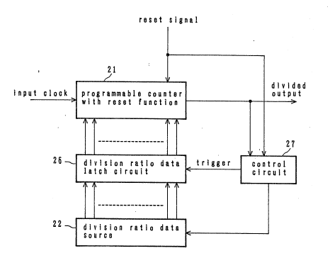
Figure 10 is a block diagram to show ~he first
embodiment of this invention programmable frequency divider
15c
.290407
27341-10
circuit. The re~erence numeral 21 denotes a programmable counter
with reset function, and 22 a diviæion ratlo data generator. The
re~erence numeral 26 denotes a division ratio data latch circuit
which temporarily retainæ the divi~lon ratio data outputted from
the
15d
:-: .. . .
~2~0407 21341 10
generator 22 and sends the data to the programmable counter 21
when a trigger signal is received, and 27 a control circuit.
Figure 11 shows a timing chart of the preset operation of
this embodiment. When it is reset, the output from the program-
mable counter 21 is either at a high level or a low level. In
the meanwhile, the division ratio _ generated by the generator
22 is set at the latch circuit 26, then a trigger signal is fed
to the latch circuit 26 to set the division ratio at n in the
programmable counter 21.
When the reset is released and a frequency dividing operation
is started, the operation is conducted with the division ratio
of _ for the first cycleO By the time the internal condition
progresses by the number n inside the programmable counter 21 a
new division ratio m is generated by the generator 22. When the
counting of the nth input clock is detected, a trigger signal is
fed to the latch circuit 26, and the division ratio of the pro-
grammable counter 21 is changed to _ within a cycle of input
clocks.
The frequency is thereEor divided with the ratio _ in the
second cycle and thereafter.
If _ is selected arbitrarily in the above operation, the
first cycle can be made programmable, and the initial phase at
the time of releasing the res~t can be adjusted in the unit of
input clock cycles. The programmable counter has the output sig-
nals e~uivalent to the preset function as it is of a low level
for only one cycle of input clocks and the duty ratio is negli-
gible.
16
)4~7
273~1-10
In this em~odiment, the latch circuit 26 stores temporarily
the division ratio data and supplies the same to the programmable
counter 21 at a timing not to cause malfunctioning of the pro-
grammable counter 21. The latch circuit 26 is, however, not al-
ways necessary. For instance, the division ratio data generated
from the data generator 22 may be directly supplied to the pro-
grammable counter 21 if the division ratio data is to be taken
only,when the reset state is released, or when a dividing oper-
ation for one cycle is completed.
Figure 12 is a block diagram to show the second embodiment
of this invention programmable frequency divider.
~9~:)4~:)7
In thls embodiment, instead of the programmable
counter 21 with reset ~unction, a pulse swallow typ~
programmable counter 25 comprising a pre scaler 24
which can switch the division ratio between P and P+L,
and a programmable counter 23 (with reset unction)
incorporatin~ a counter A (division ratio a) and a counter
s (division ratio b) is used. The pulse swallow type
programmable counter 25 is similar to a well known
counter capable o~ the operations mentioned above.
FIG. 13 shows a timing chart of the preset opera-
tion o~ this embodiment. When the pre-scaler 24 and the
programmable counter 23 are reset simultaneously, the
outputs from the pre-scaler 24 and the counter 23 are
set at either a high level or a low level. Meanwhile,
the division ratio n is set by the data generator 22 !
and a trigger signal is fed to the latch circuit 26.
Then the division ratio of the pulse swallow type
programmable counter 25 comprising the pre-scaler 24
and the programmable counter 23 is set at n, and the
division of the pre-scaler 24 is set at P~l simultaneously.
More specifi.cally, the counter ~ within the pro-
grammable counter 23 is for changing the division ratio
of the pre-scaler 24 and does not concern the division
ratio of the whole system. When it receives the
division ratio data n from the latch circuit 26, the
counter 25 adjusts the division ratio for the pre-scaler
~90407
27341-lO
24 and the counter B in a manner to make the division ratio of
the system n. Therefore, the latch circuit 26 may be the same
circuit as the one used in the first embodiment.
After the reset is released and th~ dividing operation
starts, the pulse swallow type programmable counter 25 divides
frequency for the first cycle by counting the number _ of input
clocks while changing the division ratio of the pre-scaler 24
fro~ P~l to P. The counter B of the colmter 23 counts the out-
put pulses in the number _ of the pre-scaler 24 (provided that
n = bP + a.)
In the dividing operation, by the time the programmable
counter 23 has counted the b number of the output pulses of the
pre-scaler 24, the control circuit 24 newly generates a di~ision
ratio m at the data generator 23. Subsequently, the control
circuit 24 detects that the circuit 23 has counted the _ number
of output pulses from the pre-scaler 24, feeds a trlgger signal
to the latch circuit 26, and changes the division ratio of the
counter 25 to m within one cycle of the output pulses of the
pre-scaler 24. The pulse swallow type proyrammable counter 25
conducts dividin~ operation with the division ratio _ from the
second cycle and thereon.
By selecting the number _ arbitrarily, it is possible to
change the cycle of dividing operation of the first cycle in the
counter 25, and to adjust the initial phase by the unit of the
clock cycles inputted from the pre-scaler 24 after the reset is
released.
The time allo~able from the time the output is triggered
for the first c~cle and to the change of division ratio to m at the
19
~2904~ 27341-10
programmable counter 21 is within one cycle of the input clocks
in the first embodiment. In the second embodiment, on the other
hand, the allowable time of the pulse swallow type counter 25-is
equivalent to one cycle of input clocks of the circuit 23 or the
value equi~alent to P~l times of the input clock of the pxe-
scaler 24.
If the input clocks are identical in the first and second
embodiments, therefore, the allowable time of the second embodi-
ment becomes P+l times as much as the first embodiment.
Similarly to the first embodiment, as the cycle of the di~id-
ing operation can be changed from the first cycle in the unit of
clock cycle in this embodiment, it can achieve the effect similar
to the preset function.
If the second embodiment is used as the programmable fre-
quency divider 2 of the frequency synthesizer shown in Figure 1,
when the delay is caused by the gate circuit from detection of
output signals of the reference oscillator 3 by the controller
8 and reset of the circuit 2 (generally in the order of several
tens nsec). The initial phase of the pre-scaler and the pro-
grammable counter outputs can be adjusted in the unit of the in-
put cloc]c cycles. This causes offsetting of the delay witnout
an analogue delay circuit.
For instance, if it is assumed that the frequency of the
voltage controlled oscillator is 1 GHz, the delay can be adjusted
for every 1 nsec (=l/lGHz).
The aforementioned programmable frequency dividing circuit
can be structured fully with digital ICs. E'urther, the whole
system of the frequency synthesizer can be integrated with ICs.
~2~ ot7
2734]-10
As described in the foregoing statement, this invention pro-
~rammable frequency divider circuit can be applied for frequency
synthesizers most appropriately, but the usage is not limited to
the above. For instance, the invention programmable frequency
divider may be used in a prior art frequency synthesizer. Other
applications are discussed below.
Figure 14 is a block diagram of an embodiment of this inven-
tio~ frequency synthesi2er. The reference numeral 1 denotes a
voltage controlled oscillator (abbreviated as VCO in the figure),
2 a variable frequency divider, 3 a reference signal oscillator,
4 a phase comparator, 5 a loop filter, 6 a switch circuit,
04~7
7 a power source, 8 control circuit, 9 a power switch
(SW), and 10 a phase detector.
The variable frequency divider2 has the preset func-
tion to conduct dividing operation with n only in the
first cycle after the~reset condition is released, and
with N in the second cycle and thereafter. The phase
detector 10 is a circuit to detect the phase difference
between the output signals from the reference signal
oscillator 3 and the output signals from the variable
frequency divider 2.
FIG. 15 is a time chart to show an example of
operation of the embodiment shown in FIG. 14.
The operation will now be described referring to
FIGs. 14 and 15.
When a loop is formed by closing the switch circuit
6 in this invention frequency synthesizer, the control
voltage of the voltage controlled oscillator 1 is latched
at the loop filter 5. The control voltage corresponds
to the oscillated signal fre.quency outputted from the
voltage controlled oscillator 1. In order to latch the
control voltage at the loop filter 5, the voltage may be
charged from outside or latched by opening the loop
after the phase lock loop has been formed.
~ efore closing the loop, the internal condition of the
variable frequency divider 2 is reset to have the divi-
sion ratio n at nl in the first phase difference detecting
': .
.
`'
~290~ 27341-10
operation, and then the condition of the variable frequency di-
vider 2 is released when a negative going edge is detected in
the outputs of the reference signal oscillator 3 to conduct the
dividing operation with n, for the first cycle alone. At the
second cycle and thereafter, the dividing operation is conducted
with N for a certain period. The cycle herein means the cycle
of the output signals from the variable frequency divider 2.
I While conducting this dividing operation, the phase detect-
or lO detects the difference in phase between the output from
the reference signal oscillator 3 and the outputs from the var-
iable frequency divider 2 having the division ratio of N. If
the phase difference is a reference value or higher, the division
ration _ is reset to n2 in the variable frequency divider 2, and
then the phase difference detection will be resumed for the sec-
ond time.
More particularly, the variable frequency divider 2 is reset
again to conduct the same operation as the first one. If the
phase difference is still above the reference value, then the
division ratio n is set at n3 to repeat the operation.
The above operation is repeated until the time the phase
difference between the output signals rom the reference oscill-
ator 3 and from the variable frequency divider 2 becomes smaller
than one cycle of the voltage controlled oscillator output signal,
and the switch circuit 6 is closed immediately after the final
detection of the phase difference to form a closed circuit.
As the phase diference becomes less than one cycle of the
input signals from the variable frequency divider 2 final detec-
tion, if a closed loop is formed immediately after that, the
......
~2910407
27341-10
fluctuation of the frequency seldom occurs to establish a stable
phase locked loop. In the subsequent intermittent operation of
the power source, the division ratio n of the variable frequency
divider remains at the value of the final phase difference detec-
tion unless the phase difference output from the detector 10 be-
comes larger than the reference value.
Figure 16 is a circuit diagram of an embodiment of the phase
difference detector 10. This may be a well known circuit com-
prising nine NAND circuits 100 which compares the phases of the
input signals A and B to output the result.
For lnstance, when the phase of an input signal A is advan-
ced ahead of the input signal B, an advance signal is outputted
to a terminal X as shown in Figure 17a while when the phase of
the input signal A is behind the input signal s, a delay signal
is outputted to a terminal Y as shown in Figure 17b. When both
phaseso~ the signals A and B coincide, neither signal is issued.
In the circuit, if the output signal from the reference sig-
nal oscillator 3 is assumed to be an input signal A and the out-
put signal from the variable frequency divider 2 is assumed to be
an input signal B, the phase of the output signals of the variable
frequency divider 2 can be detected whether it is ahead of or be-
hind the phase of the output signals of the reference oscillator.
Therefore, if this circuit is usea as the phase detector 10
shown in Figure 14 and when the phase of the output signal of the
variable frequency divider 2 is detected to be ahead of the phase
of the output signals from the oscillator 3 at the second phase
difference detection after the divison ratio _ of the variable
frequency divider 2 has been set and nl at the first phase diff-
24
.. - ~ . ~
~90407
27341-10
erence detection, n2 which .is larger than nl can be set as the
division ratio. When it is detected to be behind, n2 which is
smaller than nl should be set as the division ratio _.
The division ratio n may be set by gradually increasing/de-
creasing the value, or increasing the convergence speed of the
division ratio _ by changing the rate of change. In both cases,
the values will be converged to one single value if the value n
is controlled to be between the value ni showing the phase ahead
and the value nj showing the phase behind. Actual phase differ-
ence at the time becomes less than one cycle of input signals of
the variable frequency divider. It is about 1.3 nsec in an 800
MHz band frequency synthesizer.
Even if an allowable error + 1 is given to _ in order to en-
hance the convergence, the phase difference will remain small
enough not to generate significant frequency fluctuation~ When
a convergence test was conducted for the division ratio _ using
this phase difference detector, it was confirmed that the values
converged to one sing].e value.
Figures 18 and 19 are block diagrams to show an embodiment
of a switch circuit 6 which is provided with a charge pump cir-
cuit 62 to increase the impedance of the output.
In the circuit shown i.n Figure 18, a control c.ircuit 61 is
inserted between the phase comparator 4 and a charge pump circuit
62. In the circuit shown in Figure 19, a reset function is pro-
vided within the phase comparator 4 to reset the internal condition
of the circuit 4 so that the output signals therefrom can in-
crease the impedance of the output :Erom the charge pump circuit
62.
U407
27341-10
In order to confirm the operation by this embodiment, an
intermittent operation test was conducted with an 800 MHz band
fre~uency ~ynthesizer.
Figure 20 explains the result of the test; the frequency
fluctua-tion occurred when the power source of the variable fre-
quency divider and of reference signal oscillator was intermitt-
ently connected in an intermittent PLL operation.
As is clear from the figure, when this embodiment is not
used, the frequency fluctuated remarkably as shown in Figure 20a
with the power supply; but with the use of this embodiment, al-
most no fluctuation of frequency occurred as is evident from
Figure 2Ob.
Figure 21 shows an example of the operations where the
power is supplied intermittently by the above embodiment.
For repeatedly switching the loop ON/OFF, the switch
circuit should be opened first to latch the control voltage of
the voltage controlled oscillator immediately before the opening
of the loop at the loop filter. For the intermittent operation,
the power source of the circuit should be cut OFF for a pre
determined period. Then, the phase difEerence detection men-
tioned above is repeated more than once to set the division ratio
_ for the variable frequency divider before connecting the
switch circuit to close the loop. Similar operation is repeated
in the subsequent switching of the loop to control the phase
difference between the output from the reference oscillator and
the output from the variable frequency divider to be constantly
less than one cycle of the voltage controlled oscillator output
signal.
26
~9040~
27341-10
Especially when a phase difference larger than one cycle of
the voltage controlled oscillator output signal is generated be-
tween the output signals from the reference signal oscillator and
from the programmable counter due to fluctuations in temperature
or electric voltage after the final _ has been set to start such
an intermittent operation, this invention control is most advan-
tageous to make the phase difference constantly~less than one
cycle of the voltage controlled output signal.
Although the description in the foregoing statement is re-
lated to the case where the phase difference is reduced only by
controlling the division ratio, the same result may be attained
by insertion of a delay circuit at the point (a) in Figure 14 so
that the refere~ce signal to be supplied to the phase comparator
4 and the phase detector 10 is delayed behind the reference sig-
nal to be supplied to the control circuit 8. For that purpose,
a delay circuit suitable for the delay required by the control
circuit 8 is attached at the time of fabrication so that the
fluctuation in delay due to the fluctuation ln temperature or
electric voltage is offset by the control of the division ratio.