Language selection

Search

Patent 1290408 Summary

Third-party information liability

Some of the information on this Web page has been provided by external sources. The Government of Canada is not responsible for the accuracy, reliability or currency of the information supplied by external sources. Users wishing to rely upon this information should consult directly with the source of the information. Content provided by external sources is not subject to official languages, privacy and accessibility requirements.

Claims and Abstract availability

Any discrepancies in the text and image of the Claims and Abstract are due to differing posting times. Text of the Claims and Abstract are posted:

  • At the time the application is open to public inspection;
  • At the time of issue of the patent (grant).
(12) Patent: (11) CA 1290408
(21) Application Number: 581948
(54) English Title: MICROWAVE TUBE MODULATOR
(54) French Title: MODULATEUR POUR TUBE HYPERFREQUENCE
Status: Expired
Bibliographic Data
(52) Canadian Patent Classification (CPC):
  • 332/24
(51) International Patent Classification (IPC):
  • H03C 1/28 (2006.01)
  • H03K 3/57 (2006.01)
  • H03K 5/02 (2006.01)
  • H03K 17/691 (2006.01)
(72) Inventors :
  • EHRENHALT, DAN (United States of America)
  • GILES, GEORGE RODNEY (United States of America)
(73) Owners :
  • DRS C3 SYSTEMS, INC. (United States of America)
(71) Applicants :
(74) Agent: SMART & BIGGAR
(74) Associate agent:
(45) Issued: 1991-10-08
(22) Filed Date: 1988-11-02
Availability of licence: Yes
(25) Language of filing: English

Patent Cooperation Treaty (PCT): No

(30) Application Priority Data:
Application No. Country/Territory Date
155,983 United States of America 1988-02-16

Abstracts

English Abstract


MICROWAVE TUBE MODULATOR

ABSTRACT

Provided is a modulator having two amplifying
stages for supplying high-voltage pulses to the primary
winding of a transformer connected to a microwave
transmitter tube. The first stage uses field-effect
transistors connected in a common source configuration
to amplify input pulses to drive the second stage, which
uses field-effect transistors connected in a common gate
configuration to drive the transformer. The circuit
configuration provides a large voltage swing across the
transformer primary and a short transistor switching
time.


Claims

Note: Claims are shown in the official language in which they were submitted.


71087-190


THE EMBODIMENTS OF THE INVENTION IN WHICH AN EXCLUSIVE
PROPERTY OR PRIVILEGE IS CLAIMED ARE DEFINED AS FOLLOWS:

1. A microwave tube modulator for amplifying an electrical
input signal, said microwave tube modulator comprising: first
amplifier means, having an input receiving the electrical input
signal, an output, and a plurality of field-effect transistors
connected in a common source configuration, for amplifying the
electrical input signal to generate a first electrical output
signal, said field-effect transistors each having at least a
source, a gate, and a drain; second amplifier means, having an
input electrically coupled to the output of said first amplifier
means, and output, and a plurality of field-effect transistors
connected in a common gate configuration, for amplifying said
first electrical output signal generated by said first amplifier
means to generate a second electrical output signal, said field-
effect transistors each having at least a source, a gate, and a
drain; a storage device for storing electrical energy; first
coupling means for conducting electrical energy from said storage
device to said first amplifier means and for coupling said first
electrical output signal to the input of said second amplifier
means; and second coupling means for coupling a feedback current
representative of said first electrical output signal to said
field-effect transistors in said first amplifier means to
stabilize the gain of said first amplifier means.


2. A microwave tube modulator according to claim 1, further
comprising an input coupling device for coupling the electrical


71087-190
input signal to the input of said first amplifier means.

3. A microwave tube modulator according to claim 2, wherein
said input coupling device is a first electrical transformer.


4. A microwave tube modulator according to claim 1, wherein
said first coupling means includes a primary winding and a
secondary winding of a second electrical transformer, said primary
winding being electrically connected between said storage device
and said first amplifier means and said secondary winding being
electrically connected between a common ground and said second
amplifier means.


5. A microwave tube modulator according to claim 4, wherein
said second coupling means includes a feedback winding on said
second electrical transformer, said feedback winding being
electrically connected between a common ground and said first
amplifier means.


6. A microwave tube modulator according to claim 5, wherein
the turns ratio of said primary winding to said secondary winding
is high.


7. A microwave tube modulator according to claim 1, wherein

said storage device comprises at least one electrical capacitor.


8. A microwave tube modulator according to claim 1, wherein


71087-190
said field-effect transistors are n-channel, enhancement type,
metal-oxide silicon, field-effect transistors.


9. A microwave tube modulator according to claim 1, further
including current-sensitive means electrically connected in series
with the source of each of said field-effect transistors in said
first amplifier means and said second amplifier means for
protecting the microwave tube modulator from excessive electrical
current flowing through said field-effect transistors by
electrically removing from the microwave tube modulator any of
said field-effect transistors subjected to or causing excessive
current flow between its source and its drain.


10. A microwave tube modulator according to claim 9, wherein
said current-sensitive device comprises a fuse resistor
electrically connected in series with the source of each field-
effect transistor.


11. A microwave tube modulator for amplifying an electrical
input signal, said microwave tube modulator comprising: first
amplifier means, having an input receiving the electrical input
signal, an output, and a plurality of field-effect transistors
connected in a common source configuration, for amplifying the
electrical input signal to generate a first electrical output
signal, said field-effect transistors each having at least a
source, a gate, and a drain; a first electrical transformer for

coupling the electrical input signal to the input of said first
11

71087-190
amplifier means; second amplifier means, having an input
electrically coupled to the output of said first amplifier means,
an output, and a plurality of field-effect transistors connected
in a common gate configuration, for amplifying said first
electrical output signal generated by said first amplifier means
to generate a second electrical output signal, said field-effect
transistors each having at least a source, a gate, and a drain; a
storage device having at least one electrical capacitor for
storing electrical energy; and a second electrical transformer for
conducting electrical energy from said storage device to said
first amplifier means, for coupling said first electrical output
to the input of said second amplifier means, and for coupling a
feedback current representative of said first electrical output
signal to said field-effect transistors in said first amplifier
means to stabilize the gain of said first amplifier means.


12. A microwave tube modulator according to claim 11,
wherein said second electrical transformer has a primary winding
electrically connected between said storage device and said first
amplifier means, a secondary winding electrically connected to
said second amplifier means, and a feedback winding electrically
connected to said first amplifier means.


13. A microwave tube modulator according to claim 12,
wherein the turns ratio of said primary winding to said secondary
winding is high.
12

71087-190
14. A microwave tube modulator according to claim 11,
wherein said storage device comprises a plurality of electrical
capacitors connected in parallel.

15. A microwave tube modulator according to claim 11,
wherein said field-effect transistors are n-channel, enhancement-
type, metal-oxide silicon, field-effect transistors.


16. A microwave tube modulator according to claim 11,
wherein said first amplifier means has a plurality of field-effect
transistors connected in a common source configuration; and said
second amplifier means has a plurality of field-effect transistors
connected in a common gate configuration, the combination of said
first amplifier means, said first electrical transformer, said
second amplifier means, said storage device, and said second
electrical transformer forming an integral, microwave tube
modulator unit.


17. A microwave tube modulator according to claim 16,
wherein said integral, microwave tube modulator unit is capable of
being connected to at least one other of said integral, microwave
tube modulator units for cooperatively providing electrical power
equal to the cumulative power of all of said integral, microwave
tube modulator units so connected.


18. A microwave tube modulator according to claim 11,
further including current-sensitive means electrically connected
13

71087-190
in series with the source of each of said field-effect transistors
in said first amplifier means and said second amplifier means for
protecting the microwave tube modulator from excessive electrical
current flowing through said field-effect transistors by
electrically removing from the microwave tube modulator any of
said field-effect transistors subjected to or causing excessive
current flow between its source and its drain.

19. A microwave tube modulator according to claim 18,
wherein said current-sensitive device comprises a fuse resistor
electrically connected in series with the source of each field-
effect transistor.


20. A microwave tube modulator according to claim 1, wherein
said first amplifier means has a plurality of field-effect
transistors connected in a common source configuration, and said
second amplifier means has a plurality of field-effect transistors
connected in a common gate configuration, the combination of said
first amplifier means, said first coupling means, said second
amplifier means, said storage device, and said second coupling
means forming an integral, microwave tube modulator unit.


21. A microwave tube modulator according to claim 20,
wherein said first amplifier means has three field-effect
transistors connected in a common source configuration, and said
second amplifier means has twelve field-effect transistors
connected in a common gate configuration.


14

71087-190
22. A microwave tube modulator according to claim 20,
wherein said integral, microwave tube modulator unit is capable of
being connected to at least one other of said integral, microwave
tube modulator units for cooperatively providing electrical power
equal to the cumulative power of all of said integral, microwave
tube modulator units so connected.

23. A microwave tube modulator according to claim 16,
wherein said first amplifier means has three field-effect
transistors connected in a common source configuration, and said
second amplifier means has twelve field-effect transistors
connected in a common gate configuration.


24. A microwave tube modulator according to claim 3, wherein
said input coupling device is a first electrical transformer
having a primary winding to receive the electrical input signal
and a secondary winding connected to the input of said first
amplifier means.


Description

Note: Descriptions are shown in the official language in which they were submitted.


P-325 -1-

MICROWAVE TUBE MODUh~TOR

TECXNI Q L BAC~GROUND

This invention relates to modulators used to
provide high voltage pulses ko microwave transmitter
tube output transformers.

' BACRGROUND ART
A number of devices have been designed to
provide pulses for use in microwave modulation
applications. Some of these use field-effect
transistors ~FET's) connected in parallel, and
conventional designs use parallel FET's connected in a
common source configuration. Such a configuration
places comparative limits on the maximum voltages
available at microwave tube modulator outputs and does
not minimize the e~fect6 of drain-to-gate (Miller)
capacitance, which adversely affects FET switching
~peeds. See, for example, U.S. Patent Numbers
3,374,406; 3,374,407; 3,426,255; 3,509,567; 3,525,861;
3,544,399; 3,562,672; 3,582,975; 3,828,324: 3,914,555:
3,967,217; 3,995,178; 4,010,450; 4,071,777; 4,095,251;
4,143,387; 4,221,044; 4,235,010; 4,247,903; 4,262,296;
4,304,042; 4,328,470; 4,409,59~; 4,425,527; 4,662,058;
4,679,050; 4,679,299; 4,683,387; and 4,689,802.
The present invention provides a modulator
comprising a combination of elements that simultaneously
provides comparatively higher output voltages and
shorter output pulse rise and fall times than
conventionally configured, similarly applied, microwave
tube modulators.

~2~04~)8

P--325 --2--

DISCL05URE OF q~E INVENTION

In accordance with the presant invention, a
modulator i~ provided that is capable of supplying high-
voltage pulses having short rise and fall times to the
primary windings of appropriately selected transformers
connected to a large number of different microwave
transmitter tubes ~uch as magnetrons, pulse cavity
oscillators, cross field amplifiers and traveling wave
tubes.
The preferred embodiment of the present
invention contemplates a modulator having a first stage
u6ing a number of parallel field-effect transistors
(FE~'s) connected in a common source configuration to
amplify input pulses for driving a second stage using a
number of parallel FETIs connected in a common gate
configuration for driving a microwave transmitter tube
transformer.
The preferred embodiment of the present
invention also contemplates the use of fail-so~t means
for ensuring the survival and continued operation of the
total modulator circuit in the evant of the failure of
one or more FET's, an extremely desirable feature iE the
embodiment is to be used in remote or aircraft
installations.
The invention further contemplates a modulator
that has a relatively high switching speed.
The present invention also contemplates a
modulator that requireq a relatively low operating
voltage.
The invention also contemplates a modulator
that can, by using appropriate output transformers, be
matched to a large number o~ microwave transmitter
tubes.

~904~8

71087-1~0
The invention additionally contemplates a modulator that
can supply high-voltaye pulses having diiferent pulse widths.
The invention further aontemplates a modulator that ls
relatively small.
The invention also contemplates a modulator that is easy
to produce and maintain.
In summar~, the present invention provides a microwave
tube modulator for ampllfying an electrical input signal, sald
microwave tube modulator comprising: first amplifler means, having
an in,put receiving the electrical lnput signal, an output, and a
plurality of field-effec~ transistors connected in a common source
configuration, for ampli~ying the electrical input si~nal to
generate a first electrical output signal, said field-effect
translstors each having at least a source, a gate, and a drain;
seeond amplifier means, having an input electrically coupled to
the output of sald first amplifier means, and output, and a
plurality of field-effect transistors connected in a common gate
configuration, for amplifylng said first electrical ou~put signal
generated by said first amplifier means to generate a second
electrical output signal, said field-effect transistors each
having at least a source, a gate, and a drain; a storage device
for storing electrical energy; first coupllng means for conducting
electrical energy from said storaga device to said first amplifier
means and for coupling said first electrical output signal to the
input of said second amplifier means; and second coupling means
for coupllng a feedback aurrent representative of said first
electrical output signal to said field-effect transistors in said
first amplifier means to stabilize the gain of said first
amplifier means.
B~IEF DESCRIPTION OF THE_~RAWINGS
In the drawings, ln which like referenae characters
indicate corresponding parts in all the figures~
FIG. 1 shows, schematicall~, the microwave tube
modulator; and
FIG. ~ shows, schematically, a preferred combination of
microwave tube modulator units connected to supply high power

~.29~340~3

71~7-190
pulses to the primary circuit of a transformer connected to a
microwave transmitter tube.
DETAIL~D DESC~PTIO~ OF ~T~ PRE~ER~ED
EMBODIMENT ~ LI~
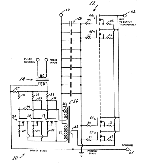
With reference to FIG. 1, shown is a schematic
representation of a microwave tube modulator unit having a first
amplifier, or driver, stage 10 and a seaond amplifier, or primary
circuit, stage 12. An input couplin~ device or first electrical
transformer 14 inductively connects an input signal or pulse
sourc~e (not shown) to the input of the first stage 10 of the
modulator, and a first coupling device, or second electrical
transformer, 16, inductively connects the output of the first
stage 10 to the input of the second stage 12.
The first, or driver, staye 10 of the modulator has, in
the embodiment shown, three field-effect transistors (FET's) 18,
19 and 20 connected in parallel in a common source configuration.
The source terminal of each of the three driver staye transistors
18, 19 and 20 is connected through one of three associated
resistors 22, 23 and 24, respectively to the common terminal 26
and is grounded. Each of the resistors 22, 23 and 24 is a fuse
resistor and will open the source circuit of its associated FET if
that transistor fails and draws excessive eurrent. This action
will effectively remove the defective transistor from the
modulator circuit, leaving the overall circuit to funation at
reduced power but otherwise in a relatively normal manner.
The secondary winding of the input trans~ormer 1~ is
electriaally shunted by a resistor 27, one end of whiah is
connected to the common terminal 26 and is yrounded. Pulses
induced in the seaondary windiny of the input transformer 14 are
applied throuyh resistors 28, 29 and 30 to the yate terminals of
the three driver staye FET's 18, 19 and 20 respectively. The gate
terminals of the FET's 18, 19 and 20 are connected through
resis~ors 32, 33 and 3~ respectively to one end of a second
coupling device, or feedback winding, 36 of the coupling
transformer 16, the other end o~ the winding 36 being connected to
ground. The drain terminals of the FET's 18, 19 and 20 are

.29~)4~)8
7~0~7-190
connected directly to one end o~ ~he primary winding 38 o~ the
coupling transformer 16, and the opposite end of the primar~
winding 38 is conneated to a source o~ positive voltaye ~as at
40), 300 volts in the embodiment shown.
The second, or primary, staye 12 of the ~odulator unit
has, in the embodiment shown, twelve power FET's (indicated by
consecutive reference numbers 44 through 55~ connected in parallel
in a common gate configuration. The secondary winding 42 of the
coupling ~ransformer 16 is connected at one end to the common
termi,nal 26 and ls grounded. Pulses induced in the secondary
winding 42 of the transformer 16 are applied ~o ~he source
terminal of each of twelve primary stage transistors (indicated by
consecutive reference numbers 44 throuyh 55) through twelve
associated reæistors (indicated by consecutive reference numbers
56 through 67 re~pectively). Each of the resistors 56 through 67
is a fuse resistor and will open the source circuit of its
associated FET i~ that transistor fails and draws excessive
current. Thls action will effectively remove the defective
transistor from the modulator circuit, leaving the overall circuit
to function at reduced power but otherwise in a relatively normal
manner.
Also connected to the source of positive voltage 40 is
one side of a storage device, or electrical capacitor bank, 68
used to store primary stage electrical charges. The other side of
the eapacitor bank 68 is connec:ted to the common terminal 26 and
is ~rounded. The gate terminal of each

~L2~040~

P-325 -6

of the twelve primary stage FETIs (indicated by
consecutive reference numbers 44 through 55) is
connected respectively to one of twelve resistors
(indicated by consecutive reference numbers 70 through
81) the other end of which is connected to the common
terminal 26 and is grounded. ~he resistors (70 through
81) minimize parasitic oscillations in the transistor
gate circuitryO The drain terminal of each of the
twPlve primary stage FET's (44 through 55) is aonnected
to an output terminal 82.
A microwave tube (not shown) connected to the
secondary winding of a suitable output transformer (also
not shown) may be coupled to the modulator by connecting
the primary winding of the transformer to the output
terminal 82.
The microwave tube modulator just described
may be advantageously combined if more power is required
than can be provided by a single unit. A typical
arrangement having four units (indicated by consecutive
reference numbers 8~ through 87) connected in parallel
is shown in FIG. 2. Their combined outputs are
connected to the primary winding of an output
transformer 88 that has a high secondary-winding-to-
primary-winding turns ratio selected to match the
voltage and current requirements of the microwave tube
to be connected to the secondary winding of the
tranaformer.
The transistors used in the embodiment shown
may be n-channel, enhancement-mode, metal-oxide silicon,
field-ef~ect transistors. An enhancement-mode type of
FET is constructed so that it effectively has no channel
until an appropriate gate voltage is applied. A direct-
current operating condition is established by applying a
positive voltage to the drain. As shown, the substrate

~9o~o~

P-325 ~7~

is connected to the source. Both are effectively at
ground potential, and channel electron~ are attracted to
the positive drain. A voltage applied to the gat2
controls the current flow. When a negative voltage i6
applied to the gate, positively charged holes from the
p-type substrate are attracted toward the gate,
effectively narrowing the conducting channel and
reduc~ng the ~ource-drain current. When a positive
voltage is applied to the gate, the positively charged
holes are repelled, effectively widening the conducting
channel and increasing the source-drain current.
Prior to the application of an input signal,
the capacitor bank connected between the source of
positive voltage 40 and ground is charged. A positive
input signal is applied through resistors 28, 29 and 30
to the gates of transistors 18, 19 and 20, making them
positive with respect to their associated sources and
enabling current to flow through the current channel
between the source and drain of each respective
transistor. This completes a path enabling electrical
energy stored in the capacitor bank 68 to flow as
current through the primary winding 38 of the coupling
transformer 16. The feedback winding 36 of the coupling
transformer 16 provides feedback current through
resistors 32, 33 and 34 to the respective gates of the
transistors 18, 19 and 20 of the driver stage 10. The
feedback acts to stabilize the gain of the driver stage
10 .
The primary-winding-to-secondary-winding turns
ratio is high, and a large current is induced into the
secondary winding 42. Since the gates of the power
transistors 44 through 55 are positive with respect to
their sources, the large current induced in the
secondary winding 42 will flow through the current

~ ~904~)8

P 325 -8-

channel between the source and drain o~ each respective
transistor and be applied to the primary winding o~ the
output transformer 88 shown in FIG. 2. This cycle is
repeated for each positive pulse applied to the input of
the modulator.
During the operation of this configuration,
khe source terminals of the power FE~Is (indicated by
consecutive reference numbers 44 through 55) may be
driven to a potential of approximately minus twenty
volts; therafore, the drain terminals of the FET's can
be driven to a potential of zero volts, providing 300-
volt pulses across the primary winding of the output
transformer.
Typical pulse voltage requirements for
microwave transmitter tubes range from 15 to 35
kilovolts. The e~bodiment of the microwave tube
modulator represented in FIG. 2 requires only 300 volts
of direct current for its operation and will supply a
current of 2600 to 3000 amperes to the primary winding
of the output transformer 88 and provide sufficient
power to operate a 250 kilowatt magnetron.
The common gate configuration of the power
transistors in the second, or primary, stage of the
modulator minimizes the e~fects of drain-to-gate
(Miller) aapacitance and thereby increases the switching
spead of the power FET ~ 8 over that obtainable by
transistors having a common source con~iguration. The
power FETI~ shown have switching times that are less
than lO0 nanoseconds.
3~

Representative Drawing
A single figure which represents the drawing illustrating the invention.
Administrative Status

For a clearer understanding of the status of the application/patent presented on this page, the site Disclaimer , as well as the definitions for Patent , Administrative Status , Maintenance Fee  and Payment History  should be consulted.

Administrative Status

Title Date
Forecasted Issue Date 1991-10-08
(22) Filed 1988-11-02
(45) Issued 1991-10-08
Expired 2008-11-02

Abandonment History

There is no abandonment history.

Payment History

Fee Type Anniversary Year Due Date Amount Paid Paid Date
Application Fee $0.00 1988-11-02
Registration of a document - section 124 $0.00 1989-04-10
Maintenance Fee - Patent - Old Act 2 1993-10-08 $100.00 1993-10-05
Maintenance Fee - Patent - Old Act 3 1994-10-10 $100.00 1994-09-14
Registration of a document - section 124 $0.00 1995-05-25
Maintenance Fee - Patent - Old Act 4 1995-10-09 $100.00 1995-07-21
Maintenance Fee - Patent - Old Act 5 1996-10-08 $0.00 1996-10-28
Maintenance Fee - Patent - Old Act 6 1997-10-08 $150.00 1997-09-25
Maintenance Fee - Patent - Old Act 7 1998-10-08 $150.00 1998-08-18
Maintenance Fee - Patent - Old Act 8 1999-10-08 $150.00 1999-08-12
Maintenance Fee - Patent - Old Act 9 2000-10-10 $150.00 2000-10-10
Registration of a document - section 124 $50.00 2000-11-14
Maintenance Fee - Patent - Old Act 10 2001-10-08 $200.00 2001-08-20
Registration of a document - section 124 $50.00 2002-04-10
Maintenance Fee - Patent - Old Act 11 2002-10-08 $200.00 2002-09-17
Maintenance Fee - Patent - Old Act 12 2003-10-08 $200.00 2003-09-24
Maintenance Fee - Patent - Old Act 13 2004-10-08 $250.00 2004-10-04
Maintenance Fee - Patent - Old Act 14 2005-10-11 $250.00 2005-10-04
Maintenance Fee - Patent - Old Act 15 2006-10-10 $450.00 2006-10-06
Registration of a document - section 124 $100.00 2006-11-06
Maintenance Fee - Patent - Old Act 16 2007-10-09 $450.00 2007-10-04
Registration of a document - section 124 $100.00 2008-08-06
Owners on Record

Note: Records showing the ownership history in alphabetical order.

Current Owners on Record
DRS C3 SYSTEMS, INC.
Past Owners on Record
DRS EW & NETWORK SYSTEMS, INC.
DRS TRAINING & CONTROL SYSTEMS, INC.
EHRENHALT, DAN
GILES, GEORGE RODNEY
LTV AEROSPACE AND DEFENSE COMPANY
SIERRA TECHNOLOGIES, INC.
SIERRATECH, INC.
Past Owners that do not appear in the "Owners on Record" listing will appear in other documentation within the application.
Documents

To view selected files, please enter reCAPTCHA code :


To view images, click a link in the Document Description column. To download the documents, select one or more checkboxes in the first column and then click the "Download Selected in PDF format (Zip Archive)" or the "Download Selected as Single PDF" button.

List of published and non-published patent-specific documents on the CPD .

If you have any difficulty accessing content, you can call the Client Service Centre at 1-866-997-1936 or send them an e-mail at CIPO Client Service Centre.


Document
Description 
Date
(yyyy-mm-dd) 
Number of pages   Size of Image (KB) 
Drawings 1993-10-22 2 48
Claims 1993-10-22 7 243
Abstract 1993-10-22 1 20
Cover Page 1993-10-22 1 13
Description 1993-10-22 8 361
Representative Drawing 2000-07-11 1 21
Fees 2006-10-06 1 34
Assignment 2006-11-06 3 75
Fees 2007-10-04 1 35
Assignment 2008-08-06 12 471
Assignment 2008-12-23 1 34
Assignment 2009-02-24 2 65
Fees 1996-10-28 1 28
Fees 1995-07-21 1 40
Fees 1994-09-14 1 39
Fees 1993-09-29 1 29