Note: Descriptions are shown in the official language in which they were submitted.
~L29~458
-1- RCA 84,836
B I T ~ S ER I AL I NTEGRATOR CIRCUITRY
This invention relates to circuitry for providing
an integration function in a gated clock, bit-ser.ial
system.
BACKGROUND OF THE INVENTION
It is known in the art of digital circuitry to
perform integration by using a delay element and an adder
circuit. The signal to be integrated is applied to one
input ~addend) of the adder circuit. The ~utput of the
adder circuit is coupled to the input of the delay element,
the ouput of which is coupled to the second input ~augend)
of the adder circuit. The integrated signal may be taken
from either the output of the adder circuit or the output
of the delay element. See for example the article by H.
Urkowitz, "Analysis and Synthesis of Delay Line Periodic
Filters," IRE Trans. on Circuit Theory, June 1957, pp
41-53.
Frequently it is desired to both scale and
truncate the values provided by the integrator. Truncation
is performed in order to reduce the number of sample bits
processed, in order to reduce the size of the processing
circuitry or minimize the processing time. It has been
found that undesirable effects may occur if the truncation
is performed in the integrator loop, that is between the
delay element and the adder. These effects are manifested
as inaccuracies in the processed signals, undesirable
excess signal build up for certain signals and possible
oscillations or limit cycles. It is an object of the
present invention to provide a bit-serial integrator
circuit which provides both scaling and truncation;
provides
integration with full bit accuracy, and requires a minimum
of hardware.
SUMMARY OF THE INVENTION
The present invention is directed to a bit-serial
integration circuit including a signal combining means
serially coupled with a~ R-stage shift register. The
output of the R-stage shift register is coupled through an
N-stage shift register to a first connection of the
.
~29~458
-2- RCA 84,836
combining means and the signal to be integrated is coupled
to a second input connection of the combining means. A
yated clock source providing at least R~N pulses per sample
period is coupled to the shift-registers to transfer sample
bits serially therethrough. Trucated, scaled and
integrated R-bit samples are available at the output
connection of the R-stage shift register.
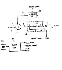
Brief Description of the Drawings
Figuxe l is a block diagram of a bit-serial
integration circuit embodying the present invention.
Figure 2 is a waveform diagram useful in
describing the invention.
Figure 3 is a bloc~ diagram of circuitry for
eliminating the DC component of a bit-serial signal5 including the integration circuit of Figure 1.
Detailed Description
The invention will be described in the
enviornment of a bit-serial gated clock system. The
samples to be processed are R-bit, ~wo's complement
bit-serial samples. Referring to Figure 2, samples occur
synchronously at a rate defined by the sample clock
designated SC. The sample bits occur synchronously with
the burst of clock pulses of the clock signal designated
CLO~K R with the least significant bit (LSB) occurring
first in time and the most significant or sign bit (MSB)
occurring last. The period o~ the burst of clock pulses of
CLOCK R is less than the sample period. The pulses of the
clocking signal CLOCK R are developed from a system clock
designated CLOCK which is a continuous waveform.
Re~erring to Figure 1, the integration circuit
includes an adder 12 having a first input terminal 10 at
which samples to be integrated are applied. The output of
the adder 12 is coupled to a sign-extend-shift-register
(SXSR) 14 including an R-stage serial shift register 16 and
a transparent latch (TL~ 18. The transparent latch 18 is
controlled by a bilevel control signal XND and passes
sample bits unaltered for signal XND in a first state and
latches the bit occurring concurrentl~ with a transition of
129045~3
-3- RCA 84,836
the signal XND going from the first state to a second state
and holds and outputs that bit for the duration that signal
XND is in the second state. The output of the transparent
latch is a scaled output of the integrated signal. The
output of the serial register 16 is coupled to an N-stage
serial shift register 22, the output o which is coupled to
a second input of adder 12. Shift registers 22 and 16 are
clocked with bursts of (R+N) clock pulses per sample period
by clock signal CLOCK (R+N) whose relationship to CLOCK (R~
is shown in Figure 2.
The control signal XND (illustrated in Figure 2)
undergoes a transition from the first to second state
during the Rth clock pulse so that the Rth sample bit
output by register 16 is latched and therefore replicated
for the remainder of the duration of the current sample
period.
The clock signals are generated by, for example,
an oscillator 23 which develops the system clock, CLOCK,
and a clock generator 24. The clock generator 24
responsive to the system clock develops the signals CLOCK
(R), CLOC~ (R+N), XND and if required signal SC. These
signals are developed in clock generator 2~ by conventional
means, the details of which are not part of this invention,
which circuitry one skilled in the art of signal processing
will readily be capable of designing knowing the timing
relationships illustrated in Figure 2.
Consider a sequence of R-bit, two's complement,
bit-serial samples being applied to input connecion 10 with
the Rth or ~ign bit of each sample replicated for the
duration of the respective sample period after the
occurrence of the R-1 value bit~. The sign bit replication
may be provided for example by applying the samples to
connection 10 via a transparent latch controlled by the
control signal XND. Assume also that the contents of
registers 16 and 22 are initially zero valued and that
adder 12 imposes no processing delay on the applied signal.
During the sample period that the first sample is applied,
since the contents of register 16 and 22 are zero valued,
1290~58
-4- RCA 84,836
the first sample passes through adder 12 unchanged and,
after the first R pulses of clock signal CLOCK (R-~N), is
resident in shift register 16. During this interval the
output OUT is zero valued, that is the zero valued contents
originally in register 16 are passed through the
transparent latch 18. Latch 18 latches ~he Rth output bit
and replicates it for the duration of the sample period
thus precluding further bit values provided by register 16,
during the sample period, from being placed on terminal
OUT.
Register 16 is clocked for an additional N clock
periods providing the N LSB's of th~ sample to the N-stage
shift register 22. At the beginning of the next sample
period, the first sample is thus available at the second
input of adder 12 and properly justified for addition to
the next applied sample. That is the LSB and subsequen~
bits of the first sample resident in register 22 will occur
coincidently with the LSB and corresponding bits of the
subseguent (second) sample applied to connection 10.
At the end of the first sample period (and every
subsequent sample period) only the R MSB's of the sum
samples are resident in register 16 since register 16 is an
R-stage register and it is clocked with R+N pulses. (Note
that even though the input samples are R-bits wide, the sum
samples can expand to R~N bits wide.) During each
subseguent sample period the R MSBIs of the sums are
provided as the output signal OUT via the transparent latch
1~. The R MSB's of the sum samples are output coincident
with the first R pulses of the burst of clock pulses. The
output samples are representative of the sum samples
provided by adder 12, truncated and shifted to N lesser
significant bit positions. The shifting of the sum samples
to N lesser significant bit positions is eguivalent to
scaling the sum samples by a factor of 2 N
The samples fed back to the adder 12 via register
22, however, are not truncated nor are they scaled. Thus
the integration is performed with full precision.
~L290458
-5- RCA 84,836
Desig~ating the values of the input samples as A,
the sum samples as B, and the samples fed back via register
22 as C, the transfer function of the circuit is derived as
follows. The sample C is e~ual to the sample B delayed by
one sample period and using conventional Z-transform
notation
C=BZ l (1)
Sum samples B are equal to
B=A+C (2)
or B=A+BZ 1 (3
collecting terms and rearranging equation (3)
B/A=l/(l-Z 1~ (4)
Equation (4) describe~ the integration function
in Z-transform notation.
Designating the output samples OUT as D
D=2-NBZ 1 (5)
and substituting (4) in (5) the transfer function D/A is
given by
D/A=2 NZ-l/(l-æ-l) (6)
indicating that the output equals the integration of the
input signal delayed one sample period and scaled by 2 N.
In the arrangement of Figure 1, the sums provided
by adder 12 may expand to bit widths of R~N since there are
a total series combination of R+N shift register stages.
Further if it is desired to feed back to adder 12, sum
samples scaled by 2 x, then the number of stages of
register 22 may be reduced by X and a transparent latch
interposed between register 22 and adder 12 which latch
being conditioned to latch and replicate the sample bit
occurring at the (R~N-X)th clock pulse.
In the Figure 1 arrangement, it was assumed that
adder 12 imposed no processing delays. If, however, adder
12 imposes Y bit periods of processing dalay, then the
samples B will be multiplied by 2 and the transfer
3S function B/A will be altered.
This factor may be partially compensated by
reducing the number of stages in register 22 by Y stages.
In this instance the transfer functions B/A and D/A are
given by
~290458
-6~ RCA 84,836
B/A=2Y/(l-Z ) (7)
and
D/A-2-(N-Y)z~ z-l) (8)
Alternatively if the adder imposes Y bit-periods
of processing delay, the transfer functions of equations
(4) and (6) can be maintained intact by increasing the
number of pulses in each burst of clock pulses by Y with no
other changes made to the circuit elements 16 and 22. In
this instance, the clock signals applied to registers 16
and 22 will contain R+N+Y pulses in each burst.
Refer next to Figure 3. The elements in Figure 3
designated with the same numbers as elements in Figure 1
are presumed identical. The circuitry in Figure 3 may be
employed to remove a DC component from a bit-serial signal
such as a bit-serial audio signal. Presume for example
that the signal applied to terminal 32 is an unsigned
straight binary signal from an analog-to--digital convertor
and all values are positive. The conversion process
inherently imposes a DC reference on the digitized signal.
The audio signal from, for example, a broadcast source is
nominally an AC signal. The DC component, if not removed,
will in general, require that the processing circuitry be
capable of processing a signal of grea~er dynamic range
than that required by the AC audio signal. Thus to
minimize the overall signal processing hardware it is
desixable to remove the DC component.
The Figure 3 circuit includes a bit-serial two's
complement subtractor circuit 30 and an integrator circuit
as d~scribed with reference to Figure 1. The input signal
(AIN) is coupled to the minuend input of the subtractor 30
and the intergrator terminal OUT is coupled to the
subtrahend input ~f the subtractor 30. Note in fact, that
the subtractor 30 and adder 12 may in fact be interchanged
if the signal ACoUT is coupled to the subtrahend input o
the subtractor interchanged with adder 12.
The signal ACoUT is equal to the difference of
the signal AIN minus the output OUT from the integrator.
The signal OUT from the integrator is, from equation (6),
129045~3
-7- RCA 84,836
OUT=ACoVT2 Nz 1/(1-2 1). (9)
Therefore,
COuT ~IN-AcouT2 Nz ~ z~1) (10)
Collecting terms and rearranging the transfer function
ACoUT/AIN of the figure 3 circuit can be shown to be
ACoUT/AIN=(Z-l)/(Z-1~2-N) (11)
For sample periods that are small relative to the signal of
interest, this transfer function contains a zero at zero ~z
and a pole at approximately 2 Nfs/2~ Hz, where fs is the
sample frequency. The audio bandwidth is 20Hz-20kHz.
Assume a sample rate of 300kHz to satisfy the criteria that
the sample period be small relative to the period of the
maximum audio-frequency. In order not to lose any of the
audio signal spectrum the pole must be at a frequency less
than 2OHz or
2 Nfs/2~ < 20. (12)
This condition is satisfied for N less than 11. For N
eq~al to 12 the 3dB point is at 11.6 Hz and for N equal to
13 the 3dB point is reduced to 5.8Hz. Thus the AC audio
signal will pass substantially with no amplitude loss and
the DC component will be completely eliminated.
Now assume that the subtractor 30 and adder 12
each impose a one-bit period delay on the signal samples.
Relative to the sample datum established in a gated clock
system, a one bit period delay effectuates a multiplication
by a factor of two. The output from subtractor 30 becomes
ACouT=2(AIN-OUT) ~13)
The signal OUT, in accordance with equation (8) becomes
OUT-ACoUT2 (N 1)z 1/(1_Z 1) (14)
Substituting (14) in (13), collecting terms and
transposing, the transfer ~unction can be shown to be
COUT/AIN=2(Z-1)/(Z_1+2-(N_2)~ (15)
Again there is a zero at zero Hertz, however, in ~his
instance the pole is at 2 (N 2)fs/2~ Hz and the amplitude
is increased by a factor of two. To establish the pole at
the same frequency as the previous example, N must be
increased by two.
~290458
-8- RCA 84,836
In the claims that follow, the phrase "burst of
clock pulses'l is recited. The "burst of clock pulses" may
occupy an entire sample period or it may occupy less than
an entire sample period depending on the particular circuit
elements selected i.e. the number of register stages and
the sample period. If the burst occupies the entire sample
period, the clock signal will occur as a continuous string
of pulses, that is, successive bursts will be immediately
adjacent one another without apparent separation. The term
"burst of clock pulses'l as used in the claims is intended
to include this contingency.