Language selection

Search

Patent 1290462 Summary

Third-party information liability

Some of the information on this Web page has been provided by external sources. The Government of Canada is not responsible for the accuracy, reliability or currency of the information supplied by external sources. Users wishing to rely upon this information should consult directly with the source of the information. Content provided by external sources is not subject to official languages, privacy and accessibility requirements.

Claims and Abstract availability

Any discrepancies in the text and image of the Claims and Abstract are due to differing posting times. Text of the Claims and Abstract are posted:

  • At the time the application is open to public inspection;
  • At the time of issue of the patent (grant).
(12) Patent: (11) CA 1290462
(21) Application Number: 578839
(54) English Title: SUBSTRATE MOUNTING DEVICE
(54) French Title: DISPOSITIF DE MONTAGE DE SUBSTRATS
Status: Deemed expired
Bibliographic Data
(52) Canadian Patent Classification (CPC):
  • 356/10
(51) International Patent Classification (IPC):
  • H05K 1/02 (2006.01)
(72) Inventors :
  • BELANGER, THOMAS D., JR. (United States of America)
(73) Owners :
  • GTE COMMUNICATION SYSTEMS CORPORATION (United States of America)
(71) Applicants :
(74) Agent: R. WILLIAM WRAY & ASSOCIATES
(74) Associate agent:
(45) Issued: 1991-10-08
(22) Filed Date: 1988-09-29
Availability of licence: N/A
(25) Language of filing: English

Patent Cooperation Treaty (PCT): No

(30) Application Priority Data: None

Abstracts

English Abstract


SUBSTRATE MOUNTING DEVICE
ABSTRACT
A substrate mounting device for installing an
electrical substrate to a carrier substrate. The substrate
mounting device includes a plurality of guide rails mounted
on the perimeter edge of the electrical substrate. First and
second substrate guides are mounted to the carrier substrate
in a spaced and parallel relationship to the other. Each
substrate guide includes a channel extending longitudinally
along a substrate guide inner side, from an open end to a top
guide. The channel is further defined by a top surface and a
plurality of drop guides which in turn form a plurality of
slots. The electrical substrate is installed by manually
inserting the electrical substrate into respective substrate
guide open ends and manually pushing the electrical substrate
along the channels until the substrate encounters a respec-
tive top guide. The top guides then urge the substrate
downward until each electrical substrate guide rail falls
into a respective substrate guide slot thereby, resting each
of the electrical substrate's plurality of guide rails on the
carrier substrate.


Claims

Note: Claims are shown in the official language in which they were submitted.


WHAT IS CLAIMED IS:
1. A substrate mounting device for mounting an
electrical substrate to a carrier substrate comprising:
a first pair of guide rails each mounted on the
perimeter edge of said electrical substrate directly opposite
each other;
a second pair of guide rails located in a spaced
relationship to said first pair of guide rails and each guide
rail of said second pair of guide rails mounted on the
perimeter edge of said electrical substrate directly opposite
each other;
first and second substrate guides mounted to said
carrier substrate in a spaced and parallel relationship to
each other, each of said substrate guides including a channel
extending longitudinally along an inner side thereof from an
open end to a top guide, said channel further defined by a
top surface and first and second drop guides, with said first
and second drop guides further defining first and second
slots;
said electrical substrate and said first and second
guide rails arranged to be manually inserted into respective
first and second substrate guide channels at respective
channel open ends and manually pushed along said channels
riding between respective first and second drop guides and
top surfaces until said substrate encounters said first and
second substrate guides top guide and each respective top
guide urges said electrical substrate downward whereby, said
first guide rail and said second guide rail fall within
respective first and second slots on each of said first and
second substrate guides thereby resting each of said first
and second electrical substrate guide rails on said carrier
substrate.
2. A substrate connector guide for mounting and
electrically connecting an electrical substrate to a carrier
substrate comprising:
first rail means mounted on a first perimeter edge


of said electrical substrate;
second rail means mounted on a second perimeter
edge of said electrical substrate directly opposite said
first rail means;
first and second guide means mounted to said
carrier substrate in a spaced and parallel relationship to
each other, each of said guide means including a channel
extending longitudinally along an inner side thereof from an
open end to a terminating end, each channel including at
least one rail means accepting slot; and,
said electrical substrate and said first and second
rails means arranged to be manually inserted into respective
first and second substrate guide means channels at respective
channel open ends and urged along each of said guide means
channels toward said closed end until said first rail means
and said second rail means fall within respective first and
second guide means slots, resting each of said first and
second rails means on said carrier substrate.
3. The substrate connector guide as claimed in
claim 2, wherein: said first rail means is a pair of guide
rails mounted in tandem and extending from the bottom surface
of said electrical substrate along a first major perimeter
edge of said electrical substrate.
4. The substrate connector guide as claimed in
claim 3, wherein: said second rail means is a pair of guide
rails mounted in tandem and extending from the bottom surface
of said electrical substrate directly opposite of said first
rail means along a second major perimeter edge of said
electrical substrate.
5. The substrate connector guide as claimed in
claim 4, wherein: each of said first and second guide means
channels is defined by a top surface and first and second
drop guides positioned in tandem along said channel, said
guide means first and second drop guides further defining
first and second slots.


6. The substrate connector guide as claimed in
?laim 5, wherein: said electrical substrate and said first
and second pair of guide rails are inserted within respective
first and second guide means channels at respective channel
open ends, and said electrical substrate is manually pushed
along each respective channel with said first and second pair
of guide rails riding between respective first and second
guide means drop guides and top surfaces until each of said
first and second pair of guide rails fall within respective
first and second guide means first and second slots.
7. The substrate connector guide as claimed in
claim 6, wherein: each of said guide means terminating ends
is a top guide extending into respective first and second
guide means channels, each top guide arranged to contact said
electrical substrate when riding within each respective
channel, thereby urging said electrical substrate in a
downward direction.
8. A substrate connector guide for mounting and
electrically connecting an electrical substrate to a carrier
substrate comprising:
rail means mounted along the major perimeter edges
of said electrical substrate;
a plurality of guide means mounted to said carrier
substrate, each of said guide means including a channel
extending longitudinally along an inner side thereof from an
open end to a terminating end, each channel including rail
means accepting slots; and,
said electrical substrate and said rails means
arranged to be manually inserted into said guide means
channel at respective channel open ends and urged along said
channels toward said closed end until said rail means fall
within respective guide means slots, resting said rails means
on said carrier substrate.


Description

Note: Descriptions are shown in the official language in which they were submitted.


~290~62

SUBSTRATE ~OUNTING DEVICE
BACKGROUND OF_THE INVENTION
This invention relates in general to modular
electronic circuit devices and more particularly to a device
for mounting electrical substrates to a carrier substrate.
In the past few years, the use of plug in units for
electrical components has found favor within the electronics
industry. Such plug-in units generally compriæe a structure
upon which are mounted electrical assemblies or sub-assem-
blies, the structure being arranged to be plugged in asuitable socket provided on a base chassis. When so plugged
the components carried by the plug-in unit are electricall~
connected in proper circuit relation to other electrical
equipment carried by the-base chassis.
Recently however, with the coming of film circuits,
the need for a specialized carrier structure for housing the
sub-assembly has disappeared. This is mainly due to the
smaller size of a film circuit. Compared to circuit fashioned
in discrete components the film circuit is appreciably
smaller and lighter. It is not uncommon to have film circuits
plugged directly into larger circuit cards or other carrier
substrates and in turn the larger substrate plugged into the
base chassis. At present, most installations of film circuits
to circuit cards is done as a permanent installation. There-
fore, removal and replacement of the film circuits though notimpossible, is a tedious and labor intensive job.
It therefor is an ob-;ect of the present invention
to disclose a new structure for mountiny, electronic sub-
strates onto carrier substrates.
SUMMARY OF THE INVENTION
In accomplishing the ob;ect of the present inven-
tion there is provided a substrate mounting device for
mounting an electrical substrate to a carrier substrate. The
electrical substrate of the present invention includes a


q~

129046;~
irst pair of guide rails each mounted on the perimeter edge
the electrical substrate directly opposite the other. A
second pair of guide rails located in a spaced relationship
from the first pair of guide rails are also mounted on the
perimeter edge of the electrical substrate directly opposite
the other.
First and second substrate guides are mounted to
the carrier substrate in a spaced and parallel relationship
to the other. Each of the first and second substrate guides
include a channel extending longitudinally along a first side
lo thereof, from an open end to a top guide. The channel is
further defined by a top surface and first and second drop
guides. The first and second drop guides further define first
and second slots.
The electrical substrate is mounted to the sub-
strate guides by manually inserting the electrical substrateinto respective first and second substrate guide channels
open ends and manually pushing the electrical substrate along
the channels. The electrical substrate and first and second
pairs of guide rails ride between respective first and second
drop guides and top surfaces. When the substrate encounters
the first and second top guides each respective top guide
urges the electrical substrate downward. The first guide rail
and the second guide rail then fall within respective first
and second slots on each of the first and second substrate
guides thereby, resting each of the first and second electri-
cal substrate guide rails on the carrier substrate.
The electrical substrate can be provided with some
means of electrical connection device which would contact or
mate with similar devices mounted on carrier the substrate.
This could provide for electrical connections batween the
electrical substrate and the carrier substrate.

~290462

BRIEF DESCRIPTION OF TH~ DRAWINGS
A better understanding of the invention may be had
from the consideration of the following detailed description
taken in conjunction with the accompanying drawinys in which:
FIG. 1 is a perspective view of a substrate having
the guide rails of the present invention installed thereon;
FIG. 2 is a perspective view of a substrate guide
of the present invention;
FIG. 3 is a top plan view of the substrate mounting
device of the present invention mounted on a carrier sub-
strate.
FIG. 4 - 7 are sectional views of the substrate
mounting device of the present invention illustrating the
manner in which a substrate is installed.

DESCRIP~ION OF THE PREFERRED EMBODIMENT
Turning now to Figs. 1 and 2 of the included
drawings the device in accordance with the invention includes
a planar substrate 10 having forward guide rails 11 and rear
guard rails 12 attached or molded onto the substrate 10 along
the edge of one of the substrates 10 major sides. A similar
set of guide rails (not shown) is also positioned on the
opposite major side of the substrate. As can be seen each
guard rail end 13 and 14 is angled so as to aid insertion and
extraction when installed into guide 20 of Fig.2.
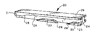
Guide 20 is a integrally molded unit comprised of a
slot or channel 24 extending longitudinally along an inner
side of guide 20. Channel 24 is defined between a planar top
cap or surface 29 and a rear drop guide 22 and forward drop
guide 23. Additionally, the channel 24 extends from an
opening at the forward end o~ the guide 20 to a top guide 27
at the rear of the guide 20. Both the forward and rear drop
guides include ramped ends 28 to aid in the positioning and
removal of the substrate 10. Further, the top guide 27
includes an angled surface 26 which also aids in the instal-

046~

'ation of substrate 10 and which will be explained in detail
~ter. Finally, guide 20 includes a generally planar bottom
surface 25 for mounting the guide to a carrier substrate.
A pair of guides 20 and 30 form the substrate
mounting device of the present invention shown in FIG. 3.
Guide 30 is a mirror image in structure to guide 20.
The substrate mounting device of the present
invention is attached by any convenient means to the top
surface of a carrier substrate 50 such as a circuit card,
backplane, or other electrical substrate.
]0 Turning now to Figs. 4 - 7 an explanation of the
installation of the substrate 10 within the substrate mount-
ing device of the present invention will be explained in
detail. It should be noted that FIGS. 4 - 7 show the instal-
lation in sectional view and therefore only guide 20 is
shown. It will be appreciated by those skilled in the art
that an identical insertion procedure occurs simultaneously
in guide 30 as the substrate is installed.
Beginning at FIG.4 the substrate 10 including rear
guide rail 12 and forward guard rail 11 is inserted into
channel 24 of guide 20 and pushed forward within the guide.
As can be seen the real rail 12 rides within the channel
between the forward drop guide 23, rear drop guide 22 and the
top cap 29. The rear guide rail 12 being longer than the rear
slot 53, which is de~ined by the rear drop guide 22 and
forward drop guide 23, rides over the forward slot 53 on
insertion.
As the substrate 10 is installed further into guide
20 substrate guide rail 11 and 12 fall into slots 53 and 52
respectively, as illustrated in FIG~ 5. This is aided by
angled surfaces 13 of guide rails 11 and 12 sliding down
angled surfaces 28 of drop guides 23 and 22.
Angled surface 26 of top guide 27 insures that
substrate 10 follows a downward motion as it is further
pushed within the guide as shown in FIG.6.
Finally, the substrate is fully installed when the

1290462

forward rail 12 and rear rail 11 rest on the carrier sub-
._rate 50 top surface within respective slots 52 and 53. The
forward end of substrate 10 rests on a top surface of bottom
member 42 when fully installed.
It will be appreciated by those skilled in the art
that the substrate 10 can be provided with some means of
electrical connection devices which would contact or mate
with similar devices mounted on carrier substrate 50. This
would provide electrical connection between substrate 10 and
the carrier substrate 50.
The substrate is easily removed by pulling the
substrate 10 out of the guide 20 in an opposite direction to
that of installation. A lifting action is provided by angled
ends 13 of substrate rails 11 and 12 riding on angled ends 28
of drop guides 23 and 22. Once the substrate 10 and rails 11
and 12 are within channel 24 the substrate is pulled and
withdrawn from the guide.
Although the preferred embodiment of the invention
has been illustrated, and that form described in detail, it
will be readily apparent to those skilled in the art that
various modifications may be made therein without departing
from the spirit of the invention or from the scope of the
appended claims.

Representative Drawing
A single figure which represents the drawing illustrating the invention.
Administrative Status

For a clearer understanding of the status of the application/patent presented on this page, the site Disclaimer , as well as the definitions for Patent , Administrative Status , Maintenance Fee  and Payment History  should be consulted.

Administrative Status

Title Date
Forecasted Issue Date 1991-10-08
(22) Filed 1988-09-29
(45) Issued 1991-10-08
Deemed Expired 2001-10-09

Abandonment History

There is no abandonment history.

Payment History

Fee Type Anniversary Year Due Date Amount Paid Paid Date
Application Fee $0.00 1988-09-29
Registration of a document - section 124 $0.00 1988-12-07
Maintenance Fee - Patent - Old Act 2 1993-10-08 $100.00 1993-10-01
Maintenance Fee - Patent - Old Act 3 1994-10-10 $100.00 1994-09-28
Maintenance Fee - Patent - Old Act 4 1995-10-09 $100.00 1995-09-28
Maintenance Fee - Patent - Old Act 5 1996-10-08 $150.00 1996-10-01
Maintenance Fee - Patent - Old Act 6 1997-10-08 $150.00 1997-09-22
Maintenance Fee - Patent - Old Act 7 1998-10-08 $150.00 1998-09-14
Maintenance Fee - Patent - Old Act 8 1999-10-08 $150.00 1999-09-08
Owners on Record

Note: Records showing the ownership history in alphabetical order.

Current Owners on Record
GTE COMMUNICATION SYSTEMS CORPORATION
Past Owners on Record
BELANGER, THOMAS D., JR.
Past Owners that do not appear in the "Owners on Record" listing will appear in other documentation within the application.
Documents

To view selected files, please enter reCAPTCHA code :


To view images, click a link in the Document Description column. To download the documents, select one or more checkboxes in the first column and then click the "Download Selected in PDF format (Zip Archive)" or the "Download Selected as Single PDF" button.

List of published and non-published patent-specific documents on the CPD .

If you have any difficulty accessing content, you can call the Client Service Centre at 1-866-997-1936 or send them an e-mail at CIPO Client Service Centre.


Document
Description 
Date
(yyyy-mm-dd) 
Number of pages   Size of Image (KB) 
Representative Drawing 2000-07-12 1 6
Drawings 1993-10-22 2 45
Claims 1993-10-22 3 154
Abstract 1993-10-22 1 33
Cover Page 1993-10-22 1 12
Description 1993-10-22 5 239
Fees 1996-10-01 1 54
Fees 1995-09-28 1 54
Fees 1994-09-28 1 54
Fees 1993-10-01 1 40