Note: Descriptions are shown in the official language in which they were submitted.
~L~9~
BACKGROUND OF THE INVENTION
The present invention is directed to a method for
generating a lattice structure with a phase skip or shift on a
surface of a substrate by exposing a photo-sensitive surface in
an optical interference field and developing the exposed surface.
For optical communications technology, special
semiconductor lasers, which also emit in a single, longitudinal
oscillatory mode at a modulation frequency, are required in order
to achieve high data rates on long transmission links. A
fundamentally suitable type of laser is the laser with a
distributed feedback which laser is referred to as a DFB-laser
wherein DFB is an abbreviation for distributed feedback and
wherein the feedback of the light in the laser resonator does not
occur by means of two mirrors but occurs by means of reflection
grating superimposed on the entire laser structure. In general,
however, a DFB-laser does not oscillate in only one mode but in
two modes. Single-mode light emission, however, can be induced
among other things by dividing the lattice structure into two
sub-gratings whose phases are shifted relative one another by
half a lattice constant, for example, by one fourth of the light
wavelength. Such DFB-lasers with the phase skip or shift are
disclosed, for example, in an article by H. Ao Haus et al
"Antisymmetric Taper of Distributed Feedback Lasersn9 IEEE
Journal of Quantum Electronics, Vol. QE-12, No. 9~ September
1976, pages 532-539
Lattice structures for DFB-lasers are currently
predominantly produced by ~olographic lithography, for example,
by exposure of a photo-resist layer applied on the surface of a
laser substrate of the semiconductor material by exposure to an
~L~9~6~
optical interference field, then developing the layer and etching
the surface covered with the developed photo-resist layer,
whereby a relief-like lattice s,tructure having a spatial
frequency corresponding to the spatial frequency of the
interference field will occur in the surface of the substrate.
The remaining steps of the laser manufacture occur in a known
manner.
The optical interference field is produced by optical
superimposition of two coherent light waveguides. However, only
simple grating structures without phase shifts will occur.
For generating a lattice structure with a phase shift;
electron beam writers are presently utilized as disclosed by an
article by X. Sekartedjo et al, "1.5 um Phase-Shifted DFB-Lasers
for Single-Mode Operation" Electronics Letters, ~ol. 20, No. 2,
January 19, 1984, pages 80-81. Another method is a holographic
lithography method with combined employment of positivP and
negative photoresist to produce the phaser shift. This method is
disclosed by K. Utaka et al, n ~ /4-Shifted InGaAsP/InP DFB
Lasers by Simultaneous Holographic Exposure of Positive and
Negative Photoresists", Electronics Letters, Vol. 20, No. 24,
November 22, 1984, pages 1008-1010. Both of these methods have
disadvantages. For example, the first method requires an
extremely costly electron beam writer. The second method
involves a technologically complicated method which leads one to
expect high rejection rates in the laser production. In both
instances, the manufacture of the lattice structure is a time
consuming process.
SUMMARY OF THE INVENTION
The object of the present invention is to provide a
particularly simple method for producing a lattice struc~ure with
a phase shift, particularly lattice structure for DFB-lasers.
This may be accomplished with an improvement in a method for
generating a lattice structure with a phase shift in a surface of
a substrate by providing a substrate having a photo-sensitive
surface, exposure of the photo-sensitive surface in an optical
interferenc~ field and by developing the exposed surface. The
improvements are that the step of exposing the photo-sensitive
surface exposes the surface to at least two superimposed
exposures of at least two different interference fields differing
in a spatial frequencies.
The method of the invention consequently differs from
the currently standard holographic lithograph for producing a
lattice structure without a phase shift for a DFB-laser
essentially only on the basis of a superposed exposure of the
photoresist in at least two optical interference fields of
different spatial fre~uencies.
In accordance with one embodiment of the invention, the
provision of the substrate with a photo-sensitive surface
provides a substrate having a photoresist layer on the suface and
the photoresist layer is developed after the superimposition of
the two exposures so that the surface of the substrate covered
with the developed photoresist layer is etched with an etchant
which attacks the surface o the substrate. In another
embodiment of the invention, the photo-sensitive surface is
composed of the substrate surface which is in contact with an
etchant and the etchant reaction thereon is activated by the
exposure. The execution or the technique of a mask-free laser-
active etchant is disclosed in an article by Ro M. Lum, F. W.
Ostermayer Jr., P. A. Kohl, A. M. Glass and A. A. Ballman in
Applied PhYsics Letter, Volume 47 No. 3, August 1985, pages 269-
~71.
The method of obtianing the two exposures of two
different interference fields differing in spatial frequencies
can be obtained in one of three ways. In one method, the photo-
sensitive surface or layer is exposed in a first interference
field of two planar, coherent waves and then a ~econd field
having different angles of incidence which is obtained by
pivoting the substrate relative to the direction of the beams
between the first and second exposure. In the second method, the
photo-sensitive surface is exposed in an interference field
formed by diverging and coherent light waves with the first
exposure being obtained with a first spacing and then moving the
substrate relative to the waves to obtain a larger or second
spacing. A final method of obtaining the different spatial
frequencies of the two interference fields is to position a
substrate relative to a mirror with the mirror and substrate
being in the path of a planar wave with portions of the wave
being reflected by the mirror onto the substrate to form the
interference. Then rotating the mirror and substrate after the
first exposure to obtain the second exposure with differ~nt
angles of incidence.
BRIEF DESCRIPTION OF THE DRAWINGS
FIG. l is a graphic representation of the defined
exposure function B(Z) for generating a lattice structure of a
DFB~laser wherein the minimum length Lmin, the optimum length
Lopt and the maximum length LmaX of the laser are specifically
related to this function;
~3~
20365-2657
Fig. 2 is a schematic illustration of the exposure of
a photoresist layer on a surface of the substrate in an
optical interference field of two optically superimposed,
planar coherent light waves;
Fig. 3 is a schematic presentation oE the exposure of
the photoresist layer on the surface of a substrate in an
interference field of two optically superimposed, divergent
coherent light waves;
Fig. 4 is a schematic illustration of the exposure of
a photoresist layer on the surface of a substrate in an
interference field of a planar light waveguide and a part of
the wave optically superimposed thereon by reElection from a
mirror; and
Fig. 5, which is located on the same drawing page as
Figure 1, is a schematic illustra-tion of the exposure of a
surface of the substrate in contact with an etching fluid
activatable by exposure wherein the exposure is the
interference field of a planar light wave and a component of
the light wave optically superimposed therewith as it is
reflected by a mirror.
DESCRIPTION OF THE PREI; ERRED EMBODIMENTS
It shall be assumed by way of an example below that a
photo-sensitive layer of a substrate, i.e. a photoresist layer
or respectively a surface of a substrate in contact with
etching fluid is double exposed in an interference field
whereby a spatial frequency K of the interEerence field is
modified by a small amount 2~K between the individual
exposures.
The exposure function Bl(Z) of a Eirst exposure, i.eO
the location dependency of the light intensity in the Z-
direction on the photo-sensitive layer may be assumed to
amount, for example, to about
(1) Bl(Z)= Bo (1 + sin (K + L~ K)Z).
Let the exposure function of the second exposure amount to
(2) B2(Z)= Bo (1 - sin (K - ~ K)Z).
The exposure function of the overall exposure is established by
~3) B(Z)= Bl(Z) + B2(Z) = Bo (2 ~ sin (K ~ a K)Z - sin (K - AK)z)
= Bol2 + 2sin(Q K Z) cos(K- Z)
This is an exposure function having the spatial fre~uency K
modulated with the modulation function sin~ R-Z. The operational
sign change of the modulation function at the locations~ K-Z =
N- can also be interpreted as a phase shift of the modulated
function at these Z-values:
cosK-Z for 2N3~ ~Z5(2N~l)
(4) B(2) ~K ~K
= 2+2 -¦ sin~K Z¦ =
Bo cos~K Z+~r) for ~2N~ ZC2N -
~ K ~K
wherein N is a whole number. The exposure function B(Z) is thus
a lattice function having a phase shift at the spacing ~ Z =~r/~
K.
The exposed photoresist layer is developed and the
lattice structure is transferred to the semiconductor material of
the substrate by etching. The remaining steps o~ the laser
manufacturing likewise occurs in a known and conventional manner.
The length L of the laser i8 selected such that a phase
shift falls into the center of the laser and such that L does not
become greater than the period LmaX = 21r/~K of the modulation
function sine ~ K-Z. On the other hand, the maximum modulation
depth of the lattice should still be reached in the laser, for
example, L should not be less than half the period Lmin of the
modulation function, i~e.
15) ~ ~ L ~ 2~r
~ K ~ K
should apply.
The product L-K ~ Lop~-K is preferably selected at about
4.6.
For a prescribed laser length L of, for example, about
500 ~m, a value of about three lines/mm thereby occurs for the
change in spatial frequency 2~ K/2~r between the two exposures.
Three expedient and advantageous embodiments of the
method of double exposure of the photo-sensitive surface of the
substrate shall be set forth with reference to FIGS. 2-5.
In these FIGS., a substrate 1 h~s a surface 11 and a
line S which extends perpendicular to the surface 11. The plane
of incidence in which the optical superposed light waves are
incident is the plane of the drawing in all FIGS. 2-5. In FIGS.
2-4, the photo-sensitive surface of the substrate 1 is composed
of a photoresist layer 2 which is applied on the surface 11.
In accordance with FIG. 2, two coherent planar waves 3
and 4 are incident from two different directions Rl and R2 and
superimposed in front of the photoresist layer 2 and form an
interference field 34 which generates interference strips on the
photoresist layer 2 which strips are parallel and proceed
perpendicular to the plane of the drawing. The spatial frequency
K of these interference strips can be set to a large degree by
the angle of incidence of the planar waves and by their
wavelength. The angle of incidence of the planar waves 3 or 4 is
established and is known by the anglesQ~ 1 and ~ 2 measured
between the allocated directions Rl and R2 and the perpendicular
line S.
In the method, the photoresist layer 2 is exposed for an
adequately long exposure time with these interference strips.
For l:he second exposure, the angle of incidenc ~ 1
and/or ~ 2 of the planar wave~ 3 and 4 is changed. This is most
6~
easily accomplished by the substrate 1 being turned around an
axis M which extends perpendicular to the plane of the paper.
For example, rotating the substrate in the direction of the arrow
R3 through an angle ~ . The modified anyles of incidence in this
case are established by ~ 1 +~ and ~ 2 ~~ . As a result
thereof, the spatial frequency K of the interference strips on
the photoresist layer 2 changes by itself. The required
change Q K in the spatial frequency can be æet by the amount of
the angle ~ by which rotation is carried out. The position of
the rotational axis M is relatively uncritical.
An embodiment of the method, which is illustrated in
FIG. 3, has two coherent, divergent waves 5 and 6 each coming
from a source point or line Q5 and Q~, respectively, these waves
5 and 6 are incident from various directions R5 and R6 and
superimposed in front of the photore~ist layer of the substrate
1. They form an interference field 56 which, likewise, generates
interference strips on the photoresist layer 2. Given prescribed
angles of incidence ~ 5 and ~ 6 of the divergent waves 5 and 6,
the spatial frequency K of these interference strips can be
largely adjusted by the spacing d of the photoresist layer from
the source points Q5 and Q6.
When the spacing d for the one exposure is selected,
then this spacing d is enlarged or, on the other hand, reduced
for the second exposure by displacement in, for example, the
direction R7 parallel to the perpendicular line S. The spatial
frequency for the interference strips on ~he photoresist layer 2,
thereby changes by itself. The required ~hange ~ K of spatial
frequency can be set by means of the spacing change ~ d.
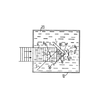
In accordance with FIG. 4, the substrate 1 is rigidly
connected to a planar mirror Sp, which is arranged relative
~o~
thereto at an angle ~ of, for example, 90. A planar wave 8 is
incident from direction R8 both directly onto the photoresist
layer 2 as well as onto the mirror 5p. The mirror Sp reflects a
component 18 of the planar wave 8, for example, half of the
planar wave incident on it into the direction of the photoresist
layer 2. An interference field 80 thus occurs in front of the
photoresist layer 2 and this interference field 80 generates
interference strips on this layer whose spatial frequency K is
dependent on the angle of incident ~ 8 of the planar wave onto
the photoresist layer 2 as well as the angle ~ between the mirror
Sp and the photoresist layer 2 or, respectively, surface 11.
When the spatial frequency K for one exposure is
selected, then a change ~K of the spatial frequency for the
second exposure can be simply set by means of the common rotation
of the substrate 1 and mirror Sp around an axis M', for example,
in the direction of the arrow Rg such as through an angle ~ '.
As is the embodiment of FIG. 2, the required change ~ K of
spatial frequency can thereby be set by the amount of the
angle ~ ' by which the rotation is carried out. Here, too, the
position of the rotation axis M' is relatively uncritical.
In FIG. 5, the photo-sensitive surface of the substrate
1 is composed of a surface 11 which is in contact with an etching
fluid 20 which is activated by exposure. Otherwise; the entire
arrangement of FIG. 5 corresponds to the arrangement of FIG. 4
whereby the mutually corresponding elements have the same
reference characters~ Differing from FIG. 4, the arrangement of
FIG. 5 is enclosed in a transparent cell 10 containing the
etching fluid 20.
The chemical reaction is triggered directly by the
substrate material at the surace 11 of the substrate due to the
6~i~
incident laser light 8. The creation of the lattice with a phase
shift proceeds in an entirely analogous fashion as given the
employment of the photoresist. In other words, during the first
exposure step, for example, the lattice having a first lattice
constant K =J~ + ~ A is produced. In the second exposure step, a
lattice having a lattice constant [K~ ~L is produced. The
lattice resulting from the superimposition of the two lattices
has a mean lattice constant~ which is sinusoidally modulated
with the period ~ J~.
Coming into consideration as etching agent are all
liquids and gasses known for laser-active etching. For example,
a mixture of one part H2S04, one part H202 and 10 parts H20, as
set orth in the above mentioned reference from ~pplied PhYs-ics
Letter, can be employed. This etchant material, for example, is
suitable or a substrate material of InP.
~ he same critical arrangement for exposure can be
employed for the manufacture of the lattice structure on the
basis of laser-active etching and for manufacture by means of
photoresist. In the method of FIG. 5~ thus, the arrangements of
either FIG. 2 or FIG. 3 can also be employed instead of the
arrangement of FIG. 4.
Al~hough various minor modifications may be suggested by
those versed in the artO it should be understood that we wish to
employ within the scope of the patent granted hereon, all such
modifications as reasonably and properly come within ~he scope of
our contribut;on to the art.
-- 10 --