Note: Descriptions are shown in the official language in which they were submitted.
~9~
~DISTRIB~T~D STATION W~LDI~G SYST~W
Technical Field
The present invention relates to welding
power supplies and in particular to improved
distributed welding power supply systems having a
single, relatively high voltage power source, and a
plurality of physically distributed power regulator~
and DC-to-DC converters for use by a plurality of
individual welders.
Backqround of the InYenti~on
The present invention is an improvement to
welding power supplies particularly suited for
environment~ in which a relatively large number of
welder~ are working in the area. The present
invention is particularly u~eful in environments in
which welding must be done in relatively small
cramped areas. In particular, the environment of a
shipyard is one in which the present invention is
particularly useful.
~ s is known to tho~e skilled in the art,
welding jobs in shipyards normally include a
relatively large number of welders welding
... .
O~g
simultaneously. Additionally, in the construction or
repair of a ship, it is often necessary for a welder
to work in relatively cramped quarters within the
interior of a ship.
s P ior art arrangements have normally
included a relatively large number of power supplies,
one for each welder. Such an arrangement i~ time
consuming and expensive since it requires multiple
drops o~ three-phase high volta~e AC line~ to supply
the various power supplies. As i9 known to those
s~illed in the art, accidental cutting of high
voltage AC power lines leads to much ~ore dangerou~
situations than similar accidentR involving the lower
voltage DC lines.
Furthermore, lack of reasonable acces3 to
the AC power lines and/or the impracticality of or
undesirability of moving the prior art power supply
sometimes creates a situation wherein the prior art
power supply is substantially removed from the welder
and a long run of welding cable i~ required. Since
the low voltage high current outputs of such welding
power supplies require large gauge cables, pulling
long runs of these cableR around a shipyard or
similar environment is cumbersome, results in
incxeased I2R losses as the cable length increa~es,
and causes variations in the quality of the weld
because of the distributed inductance, capacitance
and resistance of long runs of cable.
Additionally, the use of multiple
individual welding power ~upplLe~ necessarily mean3
duplication of one of the most expensive components
of a power supply, a large, high current three-phase
transformer.
Thus, as explained in greater detail
hereinbelow, the present invention provides a
~2~0~3~9
distributed welding power ~upply system which
overcomes ~ome of these disadvantage~. The ~ystem of
the pre~ent invention generally consist oE a single
high power regulated power supply and a plurality of
distributed weld ~elector ~tations. Within each weld
selector station there are a number of element~
es~entially ~imilar to a ~maller welding power supply.
Therefore, it is appropriate to consider other
aspects of the background of the art of solid state
welding power ~upplies in connection with the
weld ~elector stations used in the present ~ystem.
Again con~idering the environment of a
shipyard as a typical environment for welding, it i~
highly de~irable to provide a power ~upply which i~
usable in a relatively large number of welding
processesO In particular, there are a number of
variations in the electrical output characteristics
of a welding power ~upply which affect its utility in
particular welding processes. Among these are the
output impedance and the turn-on and turn-off time or
the dV/dt (dI/dt) characteri~tics of the voltage
output (current output) of the supply. For example,
in tungsten inert gas (TIG) and stick welding, it i5
generally desira~le to have a power supply with a
high output impedance so that it~ characteristics
approximate a constant current ~ource. In metal
inert gas (MIG) and pulse arc welding, it is often
desirable to have a power supply with a low output
impedance which approximate~ a con~tant voltage
source. There are, of course, other type~ of welding
which require a compromise between these
characteristics.
Another aspect of a weldlng environment
well known to those skilled in the art i9 the fact
that large transients are present in the main current
~''3~ 9
_ carrying cable~ within a welding ~yste~. The use of
pulse width modulator~ to control solid state
switching device~ to adjust output voltage has been
known in the art for some period of time. Generally,
such pulse width modulators are constructed u~ing
relatively low voltage solid state integrated
circuits. Such circuits are provided with well
regulated and well by-passed low voltage power
supplies so that they will operate properly.
One problem with prior art power ~upplie8
of thi~ type occur~ from tranQients which occur on
the DC input to a welding power supply ~witching
regulator operated by the pulse switch modulator.
When an arc is struck, there i9 normally a largs
current surge initially drawn from the output of the
power supply which normally lowers the voltage at the
input of the regula~or. ~ problem which arose in
designing a system of the present invention wa~ the
fact that multiple welders are operating weld
selector stations off of a single power ~upply output.
As variou~ welders using the system strike arc~, the
overall output voltage of the main ~upply, and thu~
the input voltage to the various weld selector
station~, will drop. Thus, it i~ desirable to
provide a feedback system for pulse width modulators
used in a distributed welding power ~upply sy~tem
which will respond to changes in the input voltage to
the weld selector ~tation.
Additionally, in some welding environments
there are a large number o~ remote welding units
which include wire feed motor~ and ~hielding gas
valves, for example, of the type shown in applicant's
U.S. Patent 4,119,830, issued october 10, 197~. The
voltage supply to the wire feed motor normally
fluctuate~ with the voltage supplied by the power
~3~ L9
supply output. Also, in some types of MIG weldinq,
the output voltage i5 lower than that required to
drive the wire feed motor. Thu~, there is a need to
as~ure that the voltage to the wire feed motor will
not become exce~sive so a~ to damage the motor or
inadequate 30 as to ~ause stalling or erratic
operation.
Furthermore, in many prior art syqtems, a
high power resiRtance box i~ used to obtain the
10 de~ired output voltage, current and impedance. These
boxes can con~ume ~ub~tantial amounts of power which
must be dissipated a3 waste heat, lower~ the ener~y
and co~t efficiency of the system, and requires
additional air f low or cooling .
LaRtly, there i~ a problem in tbe ~tate of
the prior art, not limited to the environment of
welding power supplie~, which has been overcome by
the present invention. As is well known to tho~e
skilled in the art, the design of reliable pusb-pull
20 amplif iers, whether they be linear amplifier~ or
pu~h-pull devices u3ed in switching power ~upply
regulators, ha~e always been con~idered to require
clo~ely matched pairs of output devices. Thi~ goes
back to the days of push-pull vacuum tube audio
amplifiers. In the de~ign of push-pull solid state
amplifier~, this problem ha~ become more critical
~i~ce excessive gain in one tran~i~tor of a pu~h-pull
amplifier stage normally leads to greater power
dissipation and thus a higher operating temperature
for that particular tran~istor. ~s the operating
temperature increase~, the beta of the tran~istor
tends to increase, and this ultimately lead~ to a
condition known A4 thermal run-away in which the
higher beta translqtor will be de3troyed.
As is al~o known to those skilled in the
~29~819
art, matched pairs of transistors of a particular type
tend to be considerably more expensive than individual
transistors of the same type. This cost increase becomes
even greater when relatively high current devices, such
as those used in relatively large switching power
supplies, are used. Thus, there is a need in the art to
provide a practical and reliable arrangement for
designing push-pull amplifier output stages (which may be
used in switching power supplies, linear amplifiers, and
other applications for push-pull topology) which can
eliminate the requirement for transistors having closely
matched betas and thermal characteristics.
In switching power supplies, particularly those
where push-pull operation is employed, the stress placed
upon the transistor when switching from the on state to
the off state frequently causes premature failure of the
transistors. To some degree, these failures were
alleviated by including an internal diode in the
transistor, oriented so that the diode became forward
biased if circumstances tended to cause the transistor to
operate in the inverted mode. However, this internal
diode did not fully alleviate the failure problem. In
some cases, premature failure of the switching
transistors could only be alleviated by using switching
transistors which had higher voltage and current ratings.
However, this solution increases the cost of the
switching power supply.
Therefore, there is a need for an apparatus
whlch will protect switching transistors from the
vo]tages and currents experienced in normal operation.
More particularly, -there is a need for an apparatus which
will prevent the application of excess reverse voltages
to the transistor. Also, there is a need for an
apparatus which will prevent excessive currents from
flowing through the internal diode in the switching
transistor.
L9
6a
Summary of the Invention
The present invention overcomes the drawbacks
of the prior art recited above and provides some less
expensive advantageous arrangments for accomplishing some
end results known in the prior art.
The invention in one claimed aspect pertains to
an improved welding system for conducting a plurality of
independent welding operations from a single welding
power source, comprising central power supply with
sufficient capacity to power a plurality of welding
operations and a plurality of weld parameter selection
means. Each weld parameter selecti.on means provides one
of the welding operations with electri.cal power having
selectably variable characteristics for the welding
operation, the weld parameter selection means being
powered by the central power supply. A plurality of
connecting means connects the central power supply means
to weld parameter selection means.
An improvement to the weld parameter selection
means for reducing adverse effects between the welding
operations comprise a rectifier having a first terminal
connected to a predetermined conducting means and a
second terminal connected to the power input terminal of
the weld parameter selection means, the rectifier being
for providing less noisy power to -the power input
terminal of the weld parameter selection means by
reducing electrical transients placed upon the conducting
means by other the weld parameter selection means.
An improvement to the weld parameter selection
means for reducing adverse effects between the welding
operations, also contemplates an energy storage device
connected to a predetermined conducting means and the
power inpu-t terminal of the weld parameter selection
means, the energy storage means being for providing less
38~ ~
6b
noisy power to the power input terminal of the weld
parameter selection means by reducing electrical
transients placed upon the conducting means by other weld
: parameter selection means.
A still further aspect of the invention
pertains to an improved welding power supply for
providing welding power which is compensated for
variations in input voltage, compr.ising power supply
means for providing a source of DC power, weld parameter
selection means for providing the welding power with a
selectable set of predetermined electrical parameters
desirable for a predetermined welding operation, and
conducting means for connecting the power supply means to
the weld parameter selection means. The weld parameter
selection means comprises a power input terminal, voltage
sensing means connected to the power input terminal and
responsive to the input voltage at the power input
terminal for providing an input voltage signal, and
parameter selection means responsive to the input voltage
signal for varying at least one of the predetermined
electrical parameters of the welding power.
Further the invention comprehends an improved
pulsed welding power supply, comprising pulse generating
means for providing a pulsed output signal with
predetermined electrical parameters, a power source, a
power supply output terminal, and at least one
semiconductor device responsive to the pulsed output
signal for selectively connecting and disconnecting the
power source and the power supply output terminal. The
semiconductor device has a first terminal connected to
the power source, a second term.inal connected to the
power supply output terminal, and a third termi.na] for
selectively varying the conductance between the first
terminal and the second terminal, the third terminal
being connected to the pulse generating means.
.. . . ...
A still -further aspect oE the invention
provides an electronic welder, comprising a power supply
for providing operating voltage and operating current, a
voltage divider responsive to the operating voltage for
providing a first signal, control means for providing a
second signal, a pulsewidth modulator for providing a
third signal having a pulsewidth responsive to the first
signal and the second signal, and output means responsive
to the third signal for providing welding power to a
welding operation.
Althouyh the above statements refer to broad
aspects of the invention claimed, the invention and
various other aspects disclosed are summarized herein.
More particularly, the system disclosed is a
distributed welding power supply system in which one
large relatively high voltage high power supply (80 volts
at 1500 amps continuous in the preferred embodiment) is
used to power a plurality of relatively small weld
selector station units which are essentially high current
~C to DC converters. Each weld selector station may be
operated in a constant current mode, a constant voltage
mode, or a variable combination of the two.
Additionally, each weld selector station uses a pulse
width modulated switching to control the output power
from the weld selector station. The pulse width
modulator controlling the output of each weld selector
station is arranged to respond to drops in the input
voltage rather than ~Ise of conventional arc voltage
feedback in order to maintain a nominally constant
output.
~g~9
Because each weld selector station unit is
supplied from a higher voltage source than most
conventional welding equipment, the weld selector
station may be connected the main power supply via
smaller gauge cabling than that normally u~ed to
connect a weld torch to a conventional 4t)-volt supply.
The weld selector stations of the preferred
embodiment are such that they can be readily
implemented in a small cabinet, weighing
approximately eighty pounds, which may be easily
transported into confined spaces by two people.
; ~mong the advantageou~ features of the
weld selector station of the present invention are a
switch for automatically selecting a source of input
voltage for a wire feed motor to be used with a
welding torch connected to the output of the
weld selector station. For application3 in which the
nominal output voltage from the weld selector station
is adequate to drive the wire feed motor, the wire
feed motor circuitry i5 connected directly to the
output of the weld selector station. When a lower
output voltage is selected, for example in a number
of metal inert gas (MIG) processes, the system
automatically switches the source of the wire feed
motor voltage to one of several user selectable
voltage dividers, one of which is selected to pick
off a predetermined portion of the input voltage to
the weld ~elector station.
Another advantageous aspect of the
weld selector station of the present qystem, which
applies to welding power supplies in general, i~ the
drive circuitry for the main switching transistors.
The base of the switching transistors are driven by a
pair of metal oxide semiconductor field eEfect
908~3
transi5tors (MOSFETs), one of which is a P-channel
type and one of which is an N-channel type. The FETs
have their source terminals tied together to the base
of the main switching transistor. The gates o each
s of the FETs have independently adjustable impedance~
connected between them and the source of a pulse
width modulated control signal for controlling the
output of the weld selector station. By adopting
this arrangement, the independently adju~table gate
impedances varies the rise and fall times of the
output of the main switching tran~istor~ As is
known to those skilled in the art, various welding
proce~ses respond differently to the tran~ient
characteristics of the output from the s~itching
device from a switching power supply.
Additionally, the P-channel FET i~
selectably switchable in and out of the base drive
circuit. When it is in the circuit, it causes the
base of the main switching transistor to be driven to
a voltage lower than the emitter, thus depleting
charge carriers in the base region, thereby causing
the main transistor to turn off very rapidly. When
more gradual turn-off the switching transi~tor~ is
desired, the drive to the P-channel FET may be
reduced or it may be removed from the ba~e drive
circuit.
Additionally, the present invention
includes a novel arrangement for biasing a pair of
transistors used in a push-pull configuration. In
the preferred embodiment of the present invention,
the push-pull stage in que~tion is driving the
primary of a power transformer which is used in
generating well regulated lower voltage power
supplies used to power a number of the lower voltage
integrated circuit components in the preferred
~29~)8~9
embodiment. However, the principle of this aspect of
the present invention has utility in a large number
of other applications in which power transistors are
interconnected in a fa~hion in which they need to
conduct ~ubstantially equal amount~ of average
current in order to avoid the circum~tance~ of one
transistor going into thermal run-away. For example,
push-pull power output stages in audio amplifiers may
benefit from this aspect of the present invention.
Also, parallel power transist~r conflguration~ may be
rendered less expen~ive by adoption o thi~ aspect of
the present invention.
Generally stated, thi~ aspect of the
present invention can be used to provide considerable
cost savings to the manufacturer of device~ which
normally require matched pairs of set of transistors.
As is known to those skilled in the art, matched
pairs of transistors are ones (often obtained from
the same die during fabrication) which have closely
matched characteristic~. Of particular concern is
the forward current gain or beta, of transistors
having similar or common base drives. ~g noted
above, in thepreferred embodiment, the arrangement
meeting this requirement is that of a push-pull
switching amplifier driving an inductive load.
As is known to those 3killed in the art, if
one of the transistors in such an arrangement has a
somewhat hlgher beta than the other. It will draw
more current than the other transi~tor. This leads
to a ~ituation in which the junction temperature of
the higher beta transistor becomes higher than that
of the other transistor. As junction temperature
increases, beta increases and thus the situation is
exacerbated by a form of positive feedback.
As is known to tho~e skilled in the art,
~ 9
eventually this situation lead~ to thermal run-away
and de~truction of the higher beta transistor. This
is why such amplifier arrangements are conventionally
constructed u~ing matched pairs of devices. In the
S situation of parallel drive transistors, unle~q power
wasting emitter resi~tor~ are used, one tran~istor
tends to ~hog" more current than the other~. Under
the~e circumstances, the collector-emitter saturation
voltage i8 also decreased as the transi~tor heats up,
and destruction of one o the devices often result~,
frequently followed by a chain reaction de~tructlon
of the other transi~tors as they try to accommodate
the increase in current caused by the destruction of
the first transi~tor.
The main drawback to matche~ tran~istor~,
particularly relatively high power device~, i3 that
they are much more expensive than buying a plurality
of transistors of the same type which do not
necessarily have their characteristics closely
matched, other than the extent to which they are
matched by virtue of being the same type device. ~he
present invention provides a mechanism or using
non-matched pairs of transistorq in circumstances in
which the conventional wisdom of the prior art
dictates that matched pairs be used.
Broadly stated, this aspect o~ the present
invention provides thermally sensitive base drive to
each of the transistors in questlon. Each of the
thermally sensitive base drive elements is thermally
coupled to a heat sink connected to the other
transistor of the pair. In the preferred embodiment,
each transistor includes a base emitter resistor
having a positive temperature coefficient which is
mounted on the heat sink or case of the other
transistQr. As A ~econd transistor becomes hot~er
3~
than a first transistor, the base emitter resistor of the
first transistor heats up, thus increasing its value.
This has the effect of shunting less of the input current
from the base of the first transistor, thus increasing
the first transistor's base drive. Therefore, the first
transistor begins conducting more current and the pair
moves toward an equilibrium condition.
In the preferred embodiment, a potentiometer is
connected as a variable resistor between the common
connection between the emitters of the drive transistors
and a switch. The switch is configured to selectively
connect the other end of the variable resistor to the
base of either of the drive transistors. This
arrangement is used to initially calibrate the transistor
lS pair. The switch is moved back and forth between the two
bases as the variable resistance is adjusted until an
initial condition of equality between the currents
conducted by the two transistors is established. Once
the device is subsequently operated, the above-referenced
thermal feedback connection is used to maintain this
initially established equilibrium.
Therefore, the present invention seeks to
provide an improved system for providing welding power in
an environment in which a large number of welders are
working simultaneously.
Further the present invention seeks to provide
a distributed welding power supply system employing one
master power supply and a plurality of lightweight weld
selector stations which is less expensive and more energy
efficient than provision of an equivalent amount of power
through the use of individual supplies.
Other aspects of the invention will be apparent
from the detailed description of the preferred embodiment
below.
Brie~ cr~El_on of the Dra~inq~
Fig. 1 i~ a block diagram of the preferred
embodiment of the present invention.
Fig. 2 is a block diagram of the weld
selector station of the preferred embod$ment.
Fig. 3 is ~ schematic diagram of the
switching and shutdown driver of t:he prefexred
embodiment.
Fig. 4 i~ a ~che~atic diagram of the
current detection circuits of the preferred
embodiment.
Fig. 5 is a ~chematic diagram of the STICK
& TrG control circuit of the preferred embodiment.
Fig. 6 is a s~hematic diagram o~ the low
frequency pu lsewidth m~dulator of the preferred
embodiment.
Fig. 7 is a schematic diagram of the high
frequency pulsewidth modulator of the preferred
embodiment.
Fig. 8 is a schematic diagram of the
high/low feeder voltage switchover control circuit of
the preferred embodiment.
Fig. 9 is a schematic diagram of the power
supply circuitR of the prefarred em~odiment.
Detailed Descxiption
Turning now to the drawings, in which like
numerals r'eference like elements throughout the
~everal drawings, the preferred embodiment of the
present invention will be described. As shown in
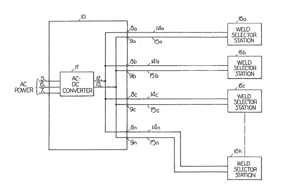
Fig. 1, the preferred form of the pre~ent invention
i9 a central welding power ~upply 10 feeding a number
of remote weld selector 3tation~ 16a 16nO Central
welding power supply 10 contain~ a single AC-to-DC
converter 11 for providing power to the weld ~elector
stations 16a-n.
~9~9
Converter 11 i8 connected to a source of
three-pha~e AC power ~not shown), normally of 460 or
230 volts, by conductors 5, 6 and 7. The positive
output of AC-to-DC converter 11 is connected by
conductor 12 to a number of po~itive output stud~
8a-8nO The negative, or return, output of converter
11 i~ connected by conductor 13 to a number of
grounded output studs 9a-9n. It will be appreciated
that the stud~ 8 and 9 are conventional in nature and
provide the connection point at the weld selector
station for the welder.
Convertar 11 provides an output of 80 volt~
DC ( nominal ) at a current ~ufficient to power the
desired number of remote weld Yelector ~tations
16a-16n. In the preferred embodiment, conver er il
provides 1500 amp~ (continuo~s) current. Method~ of
construction of central power supply 10 are well
known to those skilled in the art. Remote weld
selector stations 16a-16n are connected by conductor
L4a-14n and 15a-15n to studs 8a-8n and 9a-9n,
respectively.
Each remote weld selector station 16 can
accept an input voltage of 30 to 150 volts (80 volt~
nominal) and has its own controls for varying voltage
and current characteristic~O ~his allow~ a welder
using a remote weld selector station 16a to ad just
the voltage and current output characteristics to
match the type of welding that welder is performing
without affecting the voltage and current
characteristics of remote weld selector station~
16b-16n.
It will be appreciated the present
invention requires only a ~ingle central power supply
10 and a single AC power co~nection instead of the
multiple power supplies and AC power connections of
)8~
conventional systems. Furthermore, it will be
appreciated that since the remote weld ~elector
station 16 weighs only 80 pound~ it can be readily
moved f rom place to place as required.
S It will also be appreciat~d that, in
conventional welding systems, becau~le of the high
current~ involved, the length of the electrical cable
between power supply and welder has a ~ignificant
effect on the quality of the welding performedO ~ach
remote weld selector station 16 therefore acts as a
buffer between the central power supply 10 and the
welder. It will therefore be appreciated that the
present invention effectively reduces the length of
electrical cable to the short distance between the
remote weld selector station 16 and the welder. ~he
present invention therefore reduces the co~t of a
welding system by minimizing the amount of expsn~ive
control cable and gas hose u~ed. The pre ent
invention also reduces the cost of a welding system
20 by consolidating several smaller power supplies into
one central power supply 10 and greatly reducing the
number of AC power connection~ that must be
installed.
Weld selector statlon 16 may be briefly
described as a high efficiency, overload protected,
~electable constant current or constant voltage
switching power supply with automatic compensation
for input voltage fluctuation, and ~electable low
frequency pulse, high frequency pulse, and chopped
low frequency pulse outputs.
Turn now to Fig. 2, which i~ a block
diagram of a remote weld selector station 16. High
efficiency is obtained by the use of switching
transistors 56a-56f, inductor 62, and a free wheeling
diode 61. Transi~tors 56a-56f are rapidly switched
V~3~9
16
_ on and off to provide a desired current or voltage at
output studs 17 and 18 instead of the conventional
manner of using an array of high power di~sipation
resistors.
The positive 80 volt DC conductor 14 is
connected to the anode of a diode 20. Diode 20
protects weld selector 16 in the event that a
negative voltage is appl~ed to conductor 14. The
cathode of diode 20 is connected by conductor 21, tbe
internal po~itive 80 volt DC line, to a resistance
bar 25; the STICR & TIG control circult 30, the low
frequency pulsewidth modulator 32, the high frequency
pulsewidth modulator 34, the circuit power supplie~
38, the high/lo~ voltage switchover circuit 86, the
po~itive terminal of 10,000 microfarad ~toraye
capacitor 22, and to one end of the coil of relay 43.
Storage capacitor 22 ~tore~ power from and
ab~orbs voltage surges on VIN conductor 14 and
provides a low impedance source which can provide
large welding currents for a short period. Diode 20
also prevents capacitor 22 from discharging into VIN
conductor 14 in the event that the voltage on VIN
conductor 14 should fall below the voltage on
conductor 21. Diode 20 and capacitor 22 therefore
i801ate the output of weld selector station 16 from
transients caused by other welding operations and
rom the distributed inductance/capacitance/
resistance characteristics of conductors 14 and 15.
The ground connector 15 i8 connected to one
end of a fuse 24 and to the ground output stud 19.
The other end of fuse 24 i~ connected by conductor 23
to the negative terminal oE capacitor 22, the circuit
power supplies 38, the anode of diode 61, one end of
ON/OFF power ~witch 46, and the high/low voltage
~IL2~ 9
switchover circuit 86. The other end of switch 46 is
-
connected by conductor 47 to the other end of the
coil of relay 43. Although only a ~ingle ON/OFF
switch 46 is shown, it will be appreciated khat it i2
representative of multiple, interlocking ~witches ~o
that relay 43 may be energized/de-energized from a
local or remote location, ~uch a~ an ON/OFF ~witch on
the welding torch.
The other end of re~istance bar 25 i9
connected by conductor 42 to one contact of a
normally open pair of contact~ in relay 43. The
other contact of relay 43 is connected by conductor
44 to four snubber circuits 50a-SOd, six power
transistor circuit~ 5Sa-55f, and arc-~ustaining
resistor 45. The other end of the snubber circuit~
50a-50d, of the power transistor circuits 55a-55:E~
and of arc-sustaining resistor 45 arc connected by
conductor 41 to the cathode o diode 61, one end of
inductor 62, and the return output of shutdo~n driver
; 20 37. The other end of inductor 62 is connected by
conductor 63 to one end of resistor 64 and on,e input
of overcurrent detector circuit 73. The other end of
resistor 64 is connected by conductor 65 to the other
input of overcurrent detector circuit 73, one end of
re~istor 66, and the MIG & PUISE stud 18. The other
end of resistor 66 is connected by conductor 67 to
one end of inductor 70. The other end of inductor 70
is connected by conductor 71 to the STICR & TIG ~tud
17, one input of the high/low voltage switchover
30 circuit 86, one end of 44 ohm resistor 93 and the
input of short circuit detector circuit 72. Inductor
62 and resistor 64 provide regulation and smoothing
of the output for MIG & PULSE welding. Inductor 70
and resistor 66 provide the additional output
smoothing required for STICR & TIG welding. The
308~L9
18
other end of re~istor 93 i~ connected to 80v return
conductor 23 which is the ground for power supply 11
~Fig. 1). ~esistor 93 ha~ two tap points which are
connected by conductors 91 and 94 to two of the
iaputs of high/low voltage switchover circuit 86.
Re~i~tor 93 provides a minimum, stabilizing load for
transi~tors 56a-56f when the weld selector station 16
is on but the welder ha~ not yet struck an arc.
Re~istance bar 25 has several tap points.
The first and second tap points are connected by
conductor~ 26 and 27 to the positive and negative
inputs, respectively, of STICR & TIG control c~rcuit
30. The ~hird and fourth tap points are connected by
conductor 76 and 77 to the po~itive and negative
inputs, respeçtively, of peak current detector
circuit 80.
The output of STICR & TIG control circuit
30 is connected by conductor 31 to one input of high
frequency pulsewidth modulator 34. The output of low
frequency pulsewidth modulator 34 i9 connected by
conductor 33 to the other input of high frequency
pulsewidth modulator 34. The po itive and negative
outputs of high frequency pul~ewidth modulator 34 are
connected by conductor~ 35 and 36 to a first po~itive
and a fir~t negative input, respectively, of
switching, shutdown and driver circuit 37.
The outputs of overcurrent detector circuit
73 and 3hort circuit detector 72 are connected by
conductor 74 to one input of peak current detector 80.
The output of peak current detector 80 i~ connected
by conductor 81 to a second positive input of
switching, shutdown and driver circuit 37. The
common reference of overcurrent detector 73, short
circuit detector 72, and peak current detector 30 are
connected by conductor 75 to the second negative
~L~9~1~19
input of ~witching, shutdown and driver circuit 37.
-
The driver output and the reference outputoE switching, shutdown and driver circuit 37 are
connected by conductors 40 and 41 to th~ driver input
and reference input of power transistor circuit~
55a-55f, respectively.
The circuit power supplies 38 provide the
following output voltage to other circuit~ of the
weld selector station: + 14, +7, +15, +66.7, ~1.0~
Arc-sustaining resiRtor 45 ha~ one tap
point whlch is connected by conductor 82 to one input
of high/low voltage switchover circuit 86.
One end and the wiper of potentiometer 84
are connected by conductor 83 to a ~econd input of
high/low voltage switchover circuit 86. ~he oth~r
end of potentiometer 84 is connected by conductor 85
to a third input oE switchover circuit 86. The speed
control output~ of switchover circuit 86 are
connected by conductors 95 and 96 to the speed
control inputs of feeder control 99. The feeder
power outputs of switchover circuit 86 are connected
by conductors 95 and 96 to the feeder power inputs of
feeder control 99.
Power transi~tor circuits 55a-55f are
identical and each contain a transistor 56 and an
emitter re3istor 57. The collector of transiqtor 56
i9 connected to conductor 44. The emitter of
transistor 56a is connected to conductor 41 through
resistor S7a. The base of transistor 56a is
connected to conductor 40.
Power transistors 56a-56f are each rated at
350 volt~ and 100 amps continuous. Although ~ix NPN
transistors 56a-56~ are shown, lt will be appreciated
that the number of transistors 56 required will be
dependent upon the maximum weld current desired and
the rating~ of the individual transi~tor. It will
-
also be appreciated that PNP tran~i~tor~, field
effect tran~istor~ (FET), or other semiconductor
devices can al30 be used. At present, bipolar
transi~tor~ are preferred becau e of their higher
ratings and lower C09t.
Each power tran~istor 56 has an emitter
resi~tor 57 valued at 0.55 ohm~. It will be
appreciated that the purpose of re~istor 57 is to
prevent current-hogglng and destructive thermal
runaway by any of the parallel transistors S6. It
will also be appreciated that F~T's have a positive
resistance-temperature coefficient and do not suffer
from the ~ame type of current hogging. Therefore,
emitter resistors 57 woul~ not be required if
transistor~ 57 were an FET. However, the performance
of paralleled FET's can suffer somewhat due to
slightly differing gate characteriqtics. Therefore,
if FET'~ are u~ed for transiqtor 57 a resistor should
be placed in ~eries with the gate of each FET. The
value of the re~istor will be dependent upon the gate
characteristics of the particular F~T used.
The four snubber circuits 50a-SOd are
identical. Snubber 50a contains an 8 microfarad
capacitor 51a with one end connected by conductor 52a
to the anode of a fast recovery diode 53a and one end
of a 0.25 ohm resistor 54a. The other end of
capacitor 51a is connected to conductor 44. The
cathode of diode 53a and the other end of resistor
54a are connected to conductor 41. Snubber~ 50a-SOd
protect power transistors 56a-56f from ~witching
transients. It ~hould be noted that the value~ for
capacitor 51aand resistor 54a axe not the values that
would be obtained by the uRe of standard snubber
circuit de~ign equation~ and tables becau~e of the
~;~9~)8~9
pre~ence of arc~sustaining resistor 45.
A~ will be explained in detail below, power
transistors 56a-56f are switched on and off at a
rapid rate~ It will therefore be appreciated that
5 when tran3istor~ 56a~56f are off, there will be no
current to sustain the weLding arc and the arc will
be quenched. lrhis undesirable condition i9 preYented
by arc-sustaining resiqtor 45 connected between
conductor~ 44 and 41. Resistor 45 has a value of 2.4
10 ohms, which will pass sufficient current to keep the
welding arc alive for a short period while
transistors 56a-56f are off. When transistors
56a-56f are on, the voltage acroqs resistor 45 will
be reduced to a low value and the current supplied by
15 resistor 45 will be negligible compared to the
current conducted through transistors 56a-56f.
Arc sustaining resistor 45 also provide~ an
additional benefit. As~ume for a moment that arc
sustaining resistor 45 is not present, and that
20 transistor 56a develops a short. When driver 37
turns off tranqistors 56b-56f, the full load current
wiLl flow through transistor 56a which will, iQ most
cases, cause it to burn out and permanently become an
open circuit. When driver 37 turns transistors
25 56b-56f on again, they will have to also pas~ the
current that shou ld have been passed by transistor
56a. This extra current may cauRe transistor 56b to
fail shorted, then opened, and so on in a chain
reaction untll all six transistors have failed in the
30 open mode~
Now insert resi~tor 45. If transistor 56a
develop~ a short, then when driver 37 turns off
transistors 56b-55f, the load current will be
partially absorbed by resistor 45. This prevents
35 transistor 56a from opening and therefore prevents
~29~ .9
the chain reaction from occurring. Resistor 45 thuq
causes shorted transistor 56a to stay shorted,
instead of opening, and preserves tran~istor~
56b-56f.
5Of course, if transiYtor 56a shorts, the
weld selector ~tation 16 will not operate properly,
but the cost of repair will be reduced.
Asqume that transistors 56a-56f are on,
that the welding equipment i9 connected to the STICR
& TIG stud 17, and that welding is in progre.4~ so
that current i3 flowing through inductor~ 62 and 70
and resistors 64 and 66. It will be appreciated that
inductors 62 and 70 will oppose any rapid change in
current.
15Free wheeling diode 61, conductor 23, and
fu~e 24 therefore provide a path so that, when
transistors 56a-56f turn off, the current through
inductors 62 and 70 will decrease gradual}y instead
of instantaneously, thereby preventing a large
negative voltage from appearing on the emitter of
transistors 56a-56f. The decay rate of the current
will be determined primarily by the values of
inductors 62 and 70, reslstors 64 and 65, and the
inherent resistance, inductance, and capacitance of
the welding equipment and the arc.
Free wheeling diode 61 also protects the
weld ~elector 16 from the application of a negative
voltage to ~tuds 17 and 18. If a negative voltage is
applied to studs 17 or 18, a large current will flow
30through re~istor 64, inductor 6~, diode 61, conductor
23, and fuse 24. Fuse 24 is rated at 150 amp~. The
large current flow will blow fuse 24, thereby
isolating and protectiny the circuitry in weld
selector 16.
35Weld selector station 16 has three current
~ X~ l9
limiting circuits: peak current detector 80,
overcurrent detector 73, and short circuit detector
72. These current limiting circuit~ are explained in
detail below. The peak current detector 80 cau~e~
switching, shutdown and dri~er circuit 37 to
momentarily turn off transi~tor~ 56a-56f if the
in~tantaneou~ current exceed3 2000 ampY.
Overcurrent detector 73 cause~ driver
circuit 37 to turn off transistors 56a-56f if the
average current exceeds 300 amp~ for more than one
second. Short circuit detector 72 cause~ driver
circuit 37 to turn off transistor~ 56a-56f if the
average voltage on stud~ 17 or 18 drop~ below
approximately 4 volts. It will be appreciated that
overcurrent detector 73 and short circuit detector 72
interact. Assume that a low value re~istance is
placed across either stud 17 or 18 and stud 19 so
that an average current greater than 300 amps flo~
out of stud 17 or 18. The overcurrent detector 73
will cause transistor~ 56a-56f to be turned off. The
current will then drop and, the voltage between stud
17 or 18 and stud 19 will drop to a low value. Short
circuit detector 72 will then keep transistors
56a-56f in the off ~tate until the low value
resi~tance is removed.
The circuit power supplies 38 provide~ + 14
VDC, ~ 7 VDC, and ~15 VDC, each with an isolatecl
return, and also provide~ +66.7 VDC and ~1.0 VDC,
both having conductor 23 as a common return. Power
supplies 38 i~ described in detail below.
Switching, shutdown and driver circuit 37
is controlled by current detectors 72, 73 and 80,
pulsewidth modulator~ 32 and 34, and sTrcR ~ TIG
control circuit 30. Driver circuit 37 turns
transistors 56a-56f on and off, as required. The
_ operation of driver circuit 37 is de~cribed in detail
below.
It will be appreciated that different type~
of welding require different voltage/current
characteristics. The STICR ~ TIG mode uf welding i~
best performed with a con~tant current ~ource.
STICR fi TIG control circui~ 30 sense~ and
compensates for the current flowing through
resi~tance bar 25 90 that, if the STICR ~ TIG mode is
~elected, weld selector ~tation 16 will ~pproximate a
constant current -qource.
If the STICK h TIG control circuit 30 1~
not ~elected, weld selector 16 and stud 18
approximate a constant voltage 30urce, which i~
preferred for MIG & PULS~ type ~elding~
As previously described, weld ~elector
station 16 is a switching power supply, ~ith a
selectable switching frequency of 10 to 1500 ~z. It
will be appreciated that the type of welding and the
20 welding gas and material~ used require different
switching frequencies, waveforNs, and ~oltage-current
characteristics for best performance. Pulsewidth
modulators 32 and 34 allow the welder to select the~e
parameters. Both modulators 32 and 34, contain
circuitry which increases the output pulsewidth if
the input voltage, VIN, on conductor 14 decrease~, so
that the energy supplied to the weld remains
approximately con~tant over a large ~30 volt~ to 150
volts) range o input voltage VIN.
Low frequency modulator 32 provides an
output signal with a range of 10 to 400 Hz. 8igh
frequency modulator 34 provides an output signal with
a range of 400 to 1500 Hz. The output~ of modulator~
32 and 34 can also be combined to provide a low
frequency (5 to 400 Rz) output which is chopped at a
308~9
high frequency ~400 to 1500 Hz). This chopping
action prevent~ inductor~ 62 and 70 from saturating,
thereby improving the output regulation provided by
them. The output of either modulator 32 or 34 can be
combined with th~ output of STICR & TIG control
circuit 30 to provide a pul~ed con~tant current
~ource. In the preferred embodiment, only one or two
of the circuits 30, 32 and 34 can be activated at any
one time~
10The feeder control circuit 99 controls the
speed at which the welding material i~ fed (inched)
into the weld. Two commonly u~ed feeder control
circuits are the arc voltage feeder, which typically
requires approximately 20 to 40 volts, and the DC
controlled feeder, which typically requires
approximately 30 to 50 volts. Hish~low voltage
switchover circuit 86 automatically ~elects the
voltage on one of conductor~ 71, 82, 91 and 94 to
~aintain the proper operating voltage for feeder
control circuit 99.
A typical feeder control circuit 99 will
also have a potentiometer for varying the rate at
which the weldinq material i8 inched into the weld.
However, it will be appreciated that the welder will
desire a much lower inch feed speed when he is
adjusting the extended length of the welding material
than the inch feed speed desired during welding.
Righ/low voltage switchover circuit 86 automatically
switches the inch feed speed from the higher rate
during welding to a lower rate when welding is not
actually being performed.
Turn now to Fig. 3, which is a ~chematic
diagram of the switching, shutdown and driver circuit
37. Driver circuit 37 receives ~7 volts on conductor
35100 and -7 volts on conductor 102, both referenced to
~ 29~:)81~3
26
a 7v return conductor 101, and receive~ +14 volts on
conductor 104 and -14 volt~ on conductor 106, both
referenced to a 14v return conductor lOS.
A first positive input of driver 37 is
connected to conductor 35, and the fir~t negative
input to a first signal return conductor 36. The
~econd po itive input of driver ~7 i9 connected to
conductor 81, and the second negative input to a
second signal return conductor 7S. The output of
driver 37 is connected to conductor 40, referenced to
output return conductor 41. Driver 37 may be thought
of, in a grossly over-simplified manner, as an
electrically isolated two-input ~ND gate with the
~econd input, conductor ~1, being inverted.
- 15 Therefore, if a logic 0 voltage i5 present on
conductor 35 and/or a logic 1 i~ present on conductor
81, the output voltage on conductor 40 will be a
logic 0, selectable as 0 volts or -6 volt~.
Conversely, if a logic 1 voltage is pre~ent on
conductor 35 and a logic 0 i~ also precent on
conductor 81, the output voltage on conductor 40 will
be a logic 1, approximately +6 volts.
Referring briefly to Fig. 2, it will be
seen that conductor 40 i9 connected to the bases of
transistors S6a-56f, and conductor 41 i5 connected,
through re~istors 57a-57f, to the emitters of
transistor~ 56a-56f. Therefore, a logic 1 (+6 volts)
on conductor 40 will turn on transistors 56a-56f, and
a logic 0 will turn off transistors 56a-56f. It wlll
be appreciated that the ~tored charge in the base3 of
transi~tors 56a-56f will have a substantial effect on
their turnoff time. Some types of welding require
that the turnoff be rapid, whereas other types of
welding require a longer turnoff time. As will be
shown below, driver 37 has a selectable logic 0
~ 29(~819
output of 0 volts, which provide~ a longer turnoff
._
time, or -6 volt~, which rapidly sweeps away the base
charge and provides a rapid turnof f time .
Going back to Fig. 3, input 5ignal
S conductor 81 i5 connected through curxent limiting
re3istor 110 and conductor 111 to the anode ~ PIN 1 )
of the LED of i~oLator 112. Signal return conductor-
75 is connected to the cathode ~PIN 2) of the L~D of
isolator 112. Isolator 112 is a schmitt-trigger,
inverting, open collector optoisolator ~uch as the
MOC-5008, manufactured by Motorola, Inc., Phoenix,
Arizona. Isolator 112 contains a light emittlng
diode ~LED) ~ a photodetector, a schmitt-trigger, and
an open collector output tran~istor. The ground
terminal tPIN 5) of isolator 112 is connected to the
negative supply conductor 114. The VCC terminal ~PIN
6) of isolator 112 is connected to the output of a
regulator 130 and the positive terminal of a filter
capacitor 132l by conductor 113. The output of
regulator 130 is nominally +5 volt~ with respect to
conductor 114 and provides the 5 volt power required
for operation of isolator 112. The negative input of
regulator 130 and the negative terminal of filter
capacitor 132 are connected to the negative supply
conductor 1140 The positive input of regulator 130
i~ connected to the 14V return conductor 105. The
operation of regulator 130 is well known to those
skilled in the art.
The output ~PIN 4) of isolator 112 is
connected through the ~erles combination of conductor
115, blocking diode 116, and conductor 117 to the
cathode of a 3.6 volt zener diode 120, one end of a
resistor 121, and to the enable input (PIN 2) of a
half-bridge driver 133. A logic 1 on conductor 81
causes isolator 112 to place a logic 0 on conductor
g~38i~.~3
28
117 .
The anode of zener diode 120 i connected
to the negative ~upply conductor 114. The purpo~3e of
zener diode 120 is to assure that the voltage on
conductor 117 does not exceed the maximum rated input
voltage of half-bridge driver 133.
In the inventor ' s pro'cotype of the pre~ent
invention, driver circuit 37 wa~ in clo~e proximity
to the power ~upply circuits 38. ït wa~ determined
that transients from the power ~upply were being
coupled into isolator 112, thereby affecting it~
function. Diode 116 ~erves to prevent theE3e
tran~ients from affecting isolator 112. Diode 116 is
a Schottky diode 90 that the logic 0 voltage provided
by i~olator 112 on conductor 117 will be within the
input voltage specification for half bridge driv~er
133 .
Conductor 35 is connected to one end of a
loading reC~istor 122 and to the anode ( PIN 1~ of the
LED of isolator 123. Signal return conductor 36 i~
connected to the other end of re~istor 12 2 and to the
cathode ( PIN 2 ) of the LED of isolator 123 . Isolator
123 is an optoisolator with two out-of-phase output
transistors such a~ the M57215L, manuactured by
Mit~ubishi Electric Company, Tokyo, Japan. The
ground terminal (PIN 4) of isolator 123 is connect~d
to the negative supply conductor 114 . The f irst VCC
terminal ~ PIN 3 ) i8 connected to the +5 volt output
of regulator 130 by conductor 113. The ~econd VCC
terminal ~PIN 8) i~ connected to the 14v return
conductor 105.
The collector of the f irst output
transistor ~PIN 7) i~ connected to the 14v return
conductor 105 through current limiting resi~tor 124.
The emitter of the first output transi~tor (PXN 6)
~9~819
29
and the collector of the ~econd output transi~tor
(PIN 5) are connected together, to the other end of
resistor 121, and to one end of pulldown resistor 127
by conductor 126. The other end of re~i~tor 127 is
connected to the negative upply conductor 114. A
logic 0 on conductor 35 turn~ off the fir~t output
transistor and turns on the second output tran3istor
of isolator 123, thereby placing a logic 0 on
conductor 126.
Since i301ator 112 has an open collector
output it can only place either a logic 0 or an op~n
circuit onto conductor 117. However, i~olator 123
can place a logic O or a logic 1 onto conductor 126.
It will therefore be appreciated that if the voltage
on conductor 35 correspond~ to a logic 0 and/or the
voltage on conductor 81 corresponds to a logic 1 the
voltage on conductor 117 will correspond to a logic
0. Likewise, if the voltage on conductor 35
corresponds to a logic 1 and the voltage on conductor
81 corresponds to a logic 0, the voltage on conductor
117 will correspond to 3 logic 1.
As previously stated, conductor 117 is
connected to the enable input (PIN 2) of a
: half-bridge driver 133 ~uch aq the SG3635A
manufactured by Silicon General, Garden -Grove,
California. The pulse input (PIN 5) and the ground
terminal (PIN 3) of driver 133 are connected to
negative supply conductor 114~ The VCC input (PIN 1)
of driver 133 is connected to positive supply
conductor 136. Driver 133, as configured, functions
a~ a voltage-shifting inverter.
The output (PIN 4) of driver 133 is
connected by conductor 134 to one end of a 3.3 kilohm
load re~istor 135r the cathode of 15 volt zener diode
145, the cathode of 20 volt zener diode 163, the
~g~8~
anode of 20 volt zener diode 152, the source of
tran~istors 149 and 160, one end of a 25 ohm load
resistor 164, and output signal conductor 40. The
14v return conductor lOS is connected to the other
s end of resistor 135, to one end of switch 153, to the
cathode of 15 volt zener diode 144 and to the wiper
and one end of 400 ohm potentiometer 146. The anode
of zener diode 144 is connected to the anode of zener
diode 14S. Zener diodes 144 and 145 assure that the
10 voltage on conductor 134 does not exceed the
gate-to-source voltage of transistors 149 and 160.
The other end of potentiometer 146 i~ connected to
the gate of transistor 149 by conductor 148 through a
damping ferrite bead 147. The other end of switch
153 is connected by conductor 154 to the wiper and
one end of 400 ohm potentiometer 155. The other end
of potentiometer 155 is connected to the gate of
transistor 160 by conductor 157 through damping
ferrite bead 156.
The drain of transistor 149 is connected to
one end of a 0.425 ohm potentiometer lSl by conductor
L50. The wiper and other end of potentiometer 151
and the cathode of zener diode 152 are connected to
the +7 volt conductor 100. The drain of transistor
160 is connected to one end of a 0.05 ohm
potentiometer 162 by conductor 161. The wiper and
other end of potentiometer 162 and the cathode of
zener diode 163 are connected to the -7 volt
conductor 102. The 7v return conductor 101 is
connected to the other end of resistor 164 and the
output signal return conductor 41. Diodes 152 and
163 limit the drain to-source voltage on transistors
149 and 160, respectively.
Tran~istor 149 is an N-channel enhancement
mode power MOSPET quch as the IRF250 manufactured by
~ ~C~8~.9
~1
International Rectifier Corporation, Los ~ngeles,
California. Transistor 160 is a P~channel
enhancement mode power MOSFET ~uch as the IRF9130,
also manufactured by International Rectifier
S Corporation. As configured, transistor~ 149 and 160
function as a power inverter.
~ ssume that the voltage at the enable input
of half-bridge driver 133 corresponds to a logic 1;
driver 133 will place approximately -14 volts on
conductor 134 with respect to conductor 105. Thi3
turns on transistor 149 and turns off tran~i~tor 16Q,
thereby placing approximately ~6 volt~ on conductor
41 with respect to conductor 41. It will be
appreciated that thi turns on transistors 56a-56f of
- 15 Fig. 2.
Assume now that the voltage at the enable
input of driver 133 corresponds to a logic 0; driver
133 will place approximately +14 volt~ onto conductor
134 with respect to conductor 105. Assume also that
switch 153 is closed. This turn~ off transi3tor 149
and turns on tran istor 160, thereby placing
approximately -6 volts on conductor 40 with re~pect
to conductor 41. It will be appreciated that this
rapidly turns off transistors 56a-56f of Fig. 2 by
rapidly sweeping away any stored base charge.
However, if switch 153 is open, then both transistors
149 and 160 will be turned off, thereby placing 0
voltq an conductor 40 with respect to conductor 41.
It will be appreciated that this will turn off
3" transistors 56a-56f of Fig. 2, but at a slower rate
~ince the stored base charge decays at a ~lower rate~
The negative supply conductor 114 is
connected to the negative end of capacitor 141 and ' o
one end of potentiometer 143. The wiper and the
other end of potentiometer 143 are connected to the
~9(~1819
32
-14 volt supply conductor 106. The positive supply
conductor 136 i5 connected to the positive end of
capacitor 140 and to one end of potentiometer 142.
~he wiper and other end of potentiometer 142 are
connected to the +14 volt supply conductor 104. The
other end~ of capacitors 140 and 141 are connected to
the 14v return conductor lOS.
It will be appreciated that potentiometers
142 and 1~3 vary the maximum positive and negative
voltage, re9pectively, that driver 133 place~ on
conductor 134 and therefore vary the on-resistance of
transistors 160 and 149, respectively.
It will be noted that transi~tor~ 1~0 and
149 have a gate-to-source input capacitance of
approximately 2000 picofarads~ It will be
appreciated that potentiometer~ 155 and 146 vary the
rate at which this capacitance can be charged or
discharged and therefore vary the rate at transistor~
160 and 149, respectively, turn on and off.
. Potentiometers 151 and 162l which are in
series with the drain of transistors 149 ~nd 160,
respectively, vary the maximum current available to
turn transistors 56a-56f of Fig. 2 on and off,
respectively.
It will therefore be appreciated that
potentiometers 142, 143, 146, 155, 151 and 162, and
switch 153 allow the user to vary the switching
characteristics of tran~i~tors 56a-56f to obtain the
arc characteristics desired for the type of welding
being done.
Returning to Fig. 2, ~witching, shutdown
and driver circuit 37 is therefore controlled by the
outputs on current detectors 72, 73 and 80 on
conductors 81 and 75, and by the output of pulse
modulator 34 on conductors 35 and 36.
1;~9 [)8~.~
Resistor 164 provides additional loading
for tran~istors 149 and 160 and circuit power
supplies 38 so that the output voltage on conductor
40, with respect to conductor 41, doe~ not exceed the
allowable base-e~itter voltage of tran3i~tor~ 56a-56f
of Fig. 2.
Turn now to Fig, 4, which i~ a schematic
diagram of peak current detector 80, overcurrent
detector 73, and ~hort circuit detector 72.
10 Referring briefly to Fig. 2, peak current detector 80
causes driver circuit 37 to turn off transistor~
56a-56f whenever the current through resi~tance bar
25 exceeds the maximum rated peak curre~t for
paralleled transistor 56a-56f~ In the preferred
lS embodiment, the allowable peak current i~ 2000 amp~.
Regulator 170 ~tep~ the +15 volt~ present on
conductor 440 down to +5 voltq. The ground of
regulator 170 i~ connected to the 15v return
conductor 441. The output of regulator 170 i5
20 connected to a filter capacitor 172, the VCC terminal
(PIN 8) of current ~ense latch 176 and the driver
circuit input ~FIG. 2) by conductor 81.
Current sense latch 176 i~ a latching
comparator with a low, 0.1 volt, thre~hold, ~uch as
} 25 the SG1549 manufactured by Sllicon General, Garden
Grove, California. The "HI CM" input~ (PINS 1 and 2)
are not used and are connected to each other by
conductor 177. Current signal input conductor 76 is
connected to one end of 47 ohm re~istor 173, one end
30 of capacitor 174, and to the "LO CM ~" lnput ~PIN 3)
of latch 176~ The current signal return conductor 77
is connected to one end of a S00 ohm potentiometer
175. The wiper and the other end of potentiometer
175 are connected by the lSv return conductor 441 to
35 the other end of resistor 173, the other end of 0.02
34
microfarad capacitor 174, and the "LO CM -n/ground
~PIN 4~ of latch 176. Resi3tor 17~ and potentiometer
175 form a variable voltage divider for calibrat:ing
the peak current trip level. Capacitor 174 f ilter~
out high frequency noise.
The open collector output ~PIN 5) of latch
176 is connected to conductox 75. ~herefore, when
the input voltage (PIN 3) exceeds approximately 0.1
volt with respect to conductor 441, conductor 75 will
be shorted to conductor 441. Since conductor 81 is
connected to the +5 volt output of regulator 170,
conductor 81 will be at ~5 volt~ ta logic 1) with
respect to conductor 75. A~ previou~ly discussed, a
logic 1 on conductor 81 will cause driver 37 to turn
off transistors 56a-56f ~Fig. ~).
Referring again to Fig. 2, the current
through transistors 56a-56f al~o flows through
re~istance bar 25 and develop~ a voltage drop acros~
resistance bar 25. Conductors 76 and 77 present a
portion of this voltage to latch 176. The value of
resistance bar 25 between conductors 76 and 77 i~
approximately 0.1 volt/2000 amps = 50 microohms.
When 2000 amp~ flows through transistors 56a-56f, the
voltage between conductors 76 and 77 will be
approximat21y 0.1 volt~, thus setting latch 176 (Fig.
4) and turning off transistors 56a-56f. It will be
appreciated that a latching device was chosen for
device 176 so that a well-defined shutdown of
tran~istors 56a-56f occurs when the peak current
rating is exceeded. If a latch was not used for
device 176 then, when the peak current exceeded the
safe value, transistors 56a-56f would be turned off;
this would cause the current to quickly drop below
the safe value, which would cause tran~i~tors 56a-56f
3S to turn back on again~ cauqing the current to quickly
~.2~
ri~e above the safe value. The net re~ult would be a
high fraquency o~cillation with an average current,
instead of a peak current, of 2000 amps.
Turning back to Fig. 4, since device 176 i9
a latch there must be a mean~ to re~et it. Although
a manual reset could be used, an automatic reset i3
preferable. The output of pul~e clock 181 i~
connected by conductor 180 to the reset input (PIN 7~
o~ latch 176. In the preferred embodiment of ~he
present invention pul~e cloc~ 181 has a frequency of
60 Hz. The frequency of pulse clock 181 i~ not
critical but should be fast enough to allow weldi~g
to continue without a noticeable delay. The period
of the pulse i8 not critical, but must be at lea~lt
150 microseconds for latch 176 ~pecified to be reset~
Referring briefly to Fig. 2, ~hort circuit
detector 72 monitors the voltage on STICR & TIG stud
17 and, through resistor 66 and inductor 70, the
! voltage on ~IG & PULSE stud 18. If the voltage on
stud 17 or 18 drops below a predetermined trip
voltage because of a short circuit or because
overcurrent detector 73 has tripped, ~hort circuit
detector 72 causes switching, shutdown and driver
circuit 37 to turn off transistors 56a-56f. Short
circuit detector 72 will then keep tran~i~tors
56a-56f off until the short is removed and the
voltage at ~tuds 17 and 18 rises above the trip
voltage.
Since transistors 56a-56f are now off, they
cannot rai~e the voltage on studs 17 and 18, even
after ~he ~hort is removed. ~he re~tart voltage is
provided by the 2.4 ohm arc ~u~taining resistor 45.
It will be appreciated that resistor 45 cannot pa~
sufficient current to raise the voltage at studs 17
and 18 until the ~hort circuit is removed. Once the
~Z~308~9
36
short circuit is removed, re~istor 45 will pull studs
17 and 18 above the trip voltage and short circuit
detector 37 will allow driver circuit 37 to turn on
transistor~ 56a-56f so that welding can start again.
s Although the input of short circuit
detector 72 is shown connected to the STICR & TI~
stud 17, it will be appreciated that the input may be
connected to any point in the circuit that will have
a low voltage when stud 17 or 18 is shorted. Two of
the most likely other points are MIG & PULSE tud 18,
and conductor 67 between resistor 66 and inductor 70.
Turning back to Fig. 4, conductor 71 is
connected to the anode of blocking diode 191. The
cathode of blocking diode 101 iR connected by
: 15 conductor 192 to one end of 500 ohm resistor 193 and
to the positive terminal of 680 microfarad capacitor
194. Diode 191 allows capacitor 194 to charge, but
not to discharge, through conductor 71. The other
end of resistor 193 is connected by conductor 196 to
one end of the 12 volt, 400 ohm coil of relay 197 and
to the cathode of 15 volt zener diode 195. The other
end of the coil of relay 197, the anode of zener
: diode 195, and the negative terminal of capacitor 194
are connected to the 80v return conductor 23.
Since the coil of relay 197 is rated at 12
volt~ and the voltage on conductor 71 can be 80 volts
or more, re~istor 193 and zener diode 195 serve to
limit the voltage on the coil of relay 197~
During normal welding the voltage on
conductor 71 will be sufficient to keep relay 197
energized. However, if stud 17 and/or stud 18 are
shorted to stud 19, the voltage on conductor 71 will
be inadequate to keep relay 197 energized. Capacitor
194 serves as a holding capacitor to keep relay 197
energized for a short period of time. Thi~ prevents
~2908~9
37
short circuit detector 72 from detecting brief shorts.
During a brief short, peak current detector 80
provides protection.
If a prolon~ed short occurs, capacitor 174
will discharge through resi~tor 193, diode 195, and
the coil of relay 197, and relay 197 will be
de-en0rgized.
Relay 197 has a pair of normally closed
contacts. If a short is not present, the voltage on
conductor 71 wil1 be adequate to keep relay 197
energized, and the contacts will be open. If a
prolonged ~hort occurs, relay 197 will drop out and
the contact~ of relay 197 will closeO one contact 1~
connected to lSv conductor 441 and the other contac~t
is connected to conductor 75.
When a prolonged ~hort occurs, relay 197
will drop out, the contacts will close, and conductor
75 will be connected to conductor 441. Conductor Bl
will therefore be at ~5 volts (a logic 13 with
respect to conductor 75. As previously described, a
logic 1 on conductor 81 causes driver circuit 37
(Fig. 2) to turn off transistors 56a-56f (Fig. 2).
This condition will remain until, as
described above, the short i~ removed and the voltage
on ~tud~ 17 and 18 rises above the trip voltage.
Returning briefly to Fig. 2, overcurrent
detector 73 monitors the current flowing through
transistors 56a-56f and turns them off when the
average current exceeds the maximum rated average
current of transistors 56a-56f. In the preferred
embodiment of the present invention~ overcurrent
detector 73 i5 set to trip at 250 to 300 amps.
Assuming that the current flow is 300 amps, then
there will be approximately 0.03 ohms x 300 amps = 9
volts developed across resistor 64. This voltage is
~x~ 9
38
pre~ented to overcurrent detector 73 by conductor~ S3
and 65.
Turning now to FigO 4, conductor 63 i8
connected to one end of 25 ohm potentiometer 182.
The wiper of poten~iometer 182 i~ connected by
conductor 183 to the positive end of 4700 microfarad
capacitor 186 and to one end of the 400 ohm coil of
relay 190. Conductor 65 is connected to the other
end of potantiometer 182 and, through the series
combination o diode 184, 47 ohm resistor 185, and
conductor 187, to the other end of capacitor 186 and
the other end of the coil of relay 198.
The voltage placed between conductors 63
and 65 will, when the current exceed~ the trip value,
cause relay 190 -to pull in. Potentiometer 182 allow3
the trip point to be ~et to match the average current
rating~ of transistor 56a-56f ~Fig. 2). Re~i~tor 185
i~ a current limiting resi~tor and diode lB4 prevents
capacitor 186 from discharging through potentiometer
182 and re~istor 64.
One contact of a pair of normally open
contacts in relay 190 is connected to conductor 75.
The other contact in relay 190 i~ connected to the
15v return conductor 441. When the current flowing
through transistors 56a-56f (Fig. 2) i le~ than the
trip value relay 190 will not be energized and the
contact~ will be open. However, when the current
exceed~ the trip value, relay 190 will be energized
and the contacts of relay 190 will be clo~ed, thereby
connecting the 15v return conductor 441 to conductor
75~ ~his places ~5 volts, a logic 1, on conductor 81
with respect to conductor 75 and, as previously
described, a logic 1 on conductor 81 cause~ driver
circuit 37 ~Fig. 2) to turn off transiqtor~ 56a-56f
~Fig. 2). The current then falls below the trip
~9{~8~3
3g
value~ Capacitor 186 and the resi~tance of the coil
of relay 190 have a time constant of approximately
two second~. This a~ures that tran~istor~ 56a-56f
(Fig~ 2) are off for a ~ufficient time to causs the
output current and voltage to fall to zero~
Returning to Fig. 2, it will be appreciated
that if overcurrent detect 73 is tripped, the current
flow will be interrupted for around two econd~.
This time perivd is more than adelquate for the
voltage on stud~ 17 and 18 to fall below the trip
voltage of short circuit detector 72. Therefore,
even after the current fall~ and overcurrent detector
73 has reset, short circuit detector 72 will keep
transi tors 56a 56f turned off until the short i5
removed and resistor 45 pull~ the voltage on studs 17
and 18 back above the trip voltage.
Continuing with Fig. 2, STICK/TIG control
circuit 30 monitors the current out of studs 17 and
18 and causes weld selector 16 to function as a
con~tant current 30urce. Current flowing out of
~tud~ 17 and 18 must flow through re~istance bar 25.
One of the taps of resi~tance bar 25 i~ connected to
positive Rignal conductor 26. Another of the taps of
re~istance bar 25 is connected to the negative signal
conductor 27. Conductor~ 26 and 27 are connected to
the inputs of control circuit 30.
The voltage output of control circuit 30 on
conductor 31 increases a~ the current through
resistance bar 25 decrea~es, This causes pulsewidth
modulator 34 to increase the on-time of it~ output on
conductors 35 and 36. This causes driver circuit 30
to increase the on-time of lts output on conductors
40 and 41, thereby increasing the on-time of
transistor~ 56a-56f, which increases the output
current.
~ 3L.~3~)8~
Turn now to Fig. 5, which i~ a ~chematic
diagram of STIC~/TIG control circuit 30. Control
circuit 30 i~ powered by the +13.3 volt difference
between +80 volt conductor 21 and ~66. 7 ~olt
conductor 430, which function~ a~ the circuit ground
for control circuit 30. ~he po~iti~re signaL
conductor 26 is connected to one end of 100 ohm
resistor 221. The other end of resistor 221 is
connected by conductor 222 to one end of 100 ohm
resi~tor 212, the po~itive terminal of 100 microfarad
capacitor 213, and to one encl of 30 kilohm resi~tor
223. ~rhe other end of re~i~tor 223 i3 connected ~o
one end of 2 kilohm potentiometer 224. The other end
of potentiometer 224 is connected through 50 klloh:m
resistor 225 to circuit ground 430. The wiper of
potentiometer 224 is connected by conductor 22fi to
the non-inverting input of operational amplifier
~op-amp) 217.
The negative signal conductor 27 is
connected to one end of 100 ohm re~istor 210. The
other end of resistor 210 is connected by conductor
211 to the okher end of resistor 212, the other end
of capacitor 213, and to one end of 50 kilohm
resia~tor 214. The other end of resistor 214 is
connected by conductor 215 to one end of 500 kilohm
feedback re~i~tor 216, the inverting input of op-amp
217, and to one end of 50 kilohm resistor 220. The
other end of re~istor 216 is connected to the output
~PIN L) o~ op-amp 217 by conductor 227. The other
end of resistor 220 i~ connected to circuit grouncl
430.
It will be appreciated that op-amp 217 i~
configured as a differential-input, negative-feedback
gain stage with a gain control potentiometer 224.
Capacitor 213 i~ a ~moo'ching capacitor which
1~9(18~1.9
~1
elim~nates high f requency transient~.
The output of op-amp 217 is also connected
by conductor 227 to one end of 5.1 kilohm stabilizing
resistor 232, and one end of 5.1 kilohm resi~tor 240.
The other end of resi~tor 240 i8 connected to circuit
ground 430 through 5.1 kilohm resistor 241, and is
connected by conductor 242 to the inverting input of
op-amp 246 and one end of 30 kilohm potentiometer
243.
The ground input of op-amps 217 and 246 axe
connected to circuit ground 430. Conductor 21 i8
connected to the VCC input of op-amps 217 and 246,
and one end of 200 ohm re~i~tor 230. The other end
of resistor 230 i5 connected by conductor 231 to the
o her end of resistor 232, to the anode of
temperature compensating diode 233, and one end of
5.1 kilohm re~i~tor 235. The cathode of diode 233 is
connected to the cathode of 6.8 volt zener dic~e 234.
The anode of zener diode 234 is connected to circuit
ground 430. The other end of resistor 235 i3
connected to the non-inverting input of op-amp 246 by
conductor 237, and connected to circuit ground 430
through 5.1 kilohm re~istor 236.
Because of the temperature~ encountered in
weld ~elector 16, re~istor~ 214, 216, 220, 223, 225,
232, 235, 236, 240 and 241 should be metal film
resistors so that the output o STIC~/TIG control
circuit 30 will not be overly temperature sensitive.
It will be appreciated that diode~ 233 and
234 form a temperature-compensated 7~5 volt reference
and that resi~tors 235 and 236 p}ace one-half of this
reference voltage onto the non-inverting input of
op--amp 246.
The output of op-amp 246 i~ connected by
conductor 247 to one end and the wiper of 6.8 kilohm
~L~9V~
42
current gain limit potentiometer 244, to circuit
ground 430 through 6.3 kilohm load resistor 245, to
one end of current limiting 10 ohm re~istor 250, and
to one end of 100 kilohm re~istor 252. The other end
of limit potentiometer 244 i~ connected to the wiper
and the other end of current gain potentiometer 243.
The other end of resi~tor 250 iR connected to circuit
ground 430 through 1000 microfarad capacitor 251.
The other end of resistor 252 i~ connected to the
anode of blocking diode 253. The cathode of diode
253 is connected to output conductor 31 through
switch 254.
Op-amp 246 i~ configured as a vari ble gain
amplifier with a reference voltage ~3.7S volt~)
connected to the non-inverting inpu~ and the output
of op-amp 217 connected to the inverting input. Th~
output of op-amp 246 on conductor 247 i9 therefore
proportional to the negative of the differential
voltage between input conductors 26 and 27.
. Potentiometer~ 243 and 244 control the gain
of op-amp 246. Potentiometer 243 may be ~et by the
we~der to obtain the deqired arc characteristics.
Potentiometer 244 i5 generally not acces~ible to the
welder and is used to set ~he minimum gain sf
amplifier 246.
Capacitor 251 and re~istor 250 heavily load
the output of op-amp 246 50 that the voltage on
conductor 247 change~ at a relatively slow rate.
This assures that the output of control circuit 30 i8
re~ponsive to those variations in the welding current
caused by welding conditions and not responsive to
tho~e variations cau~ed by the normal operation of
pulsewidth modulators 32 and 34.
Returning briefly to Fig. 2, modulator 32
35 i9 a low frequency pulsewidth modulator. In the
L9
43
preferred embodiment, the pul~e frequency is variable
from approximately 10 to 400 ~z, and the duty cycle
is variable from 0 to over 90 percent. These values
are not critical but do allow the welder con~iderable
latitude for obtaining the mo t de~irable arc
characteristicq .
Modulator 32 i9 input voltage compensated.
The pulsewidth increases as the input voltage on
conductor 21 decrea~es 90 that the average power
10 delivered to the weld i9 unaffected by input volt~ge
variations.
Turn now to Fig. 6, which is a schemati~
diagram of low frequency pul~ewidth modulator 32.
Modulator 32 is powered by the 13.3 volt difference
between ~80 v~lt conductor 21 and +66. 7 volt
conduc'cor 430, which also serves as th~ circuit
ground. Conducts~r 21 i5 connected to 0.1 microfarad
capacitor 260 and to the VCCIN terminal of modulator
261. Modulator 261 is a regulating pulsewidth
modulator such as the LM3524 manufactured by ~7ational
Semiconductor Corporation, Santa Clara, California.
Modulats)r 261 contains a +5 volt regulator
262, an error tran~conductance amplifier 264, a
current limit amplifier 265, an oscillator 266, a
~hutdown control 267, a comparator 271, an
edge-triggered toggle 272, two 3-input NOR gate~ 275
and 276, and two NPN output transistor~ 277 and 280.
The output of transconductance amplifier
264, current limit amplifier 265, and shutdown
control 267 are connected to the inverting input of
compa~ator 271 by conductor 270. Current limit
amplifier 265 and ~hutdown control 267 are each able
to override the output of transconductance ampllfier
264. Current limit amplifier 26S is not used 50 its
inverting input and non-inverting input are connected
08
44
to circuit ground 430 by conductor 286 and conductor
287, respectively. Shutdown control 67 i9 al~o not
used so its input i9 connected to circuit ground 430
by conductor 290,
s Regulator 262 3tep9 the ~1303 volt~ pre~erlt
on conductor 21 (with respect to circuit ground 430)
down to +5 volt~ and places thi~ regulated +5 volt~
onto conductor 263. This +5 volts al30 powers some
of the internal circuitry of modulator 261. The
input of regulator 262 i~ connected to conductor 21.
The ground terminal of modulator 26L is connected by
conductor 2B5 to circuit ground 430.
The output of o~cillator 266 is cor~ ctea
by conductor 273 to the togqle input of toggle 272
and one input of ~OR gate~ 275 and 276. The Q output
of toggle 272 i~ connected by conductor 281 to a
second input of NOR gate 275. The negated Q output
of toggle 272 i~ connected by conductor 282 to a
second input of NOR gate 276. The outpu~ of
comparator 271 is connected by conductor 274 to the
third input of NOR gates 275 and 276. The outputs of
NOR gates 275 and 276 are connected to the bases of
transistor~ 277 and 2û0, respectively. The
collector~ of tran istor3 277 and 280 are connected
to +5 volt conductor 263. The emitters of
transi~t~rs 277 and 280 are connected to output
signal conductor 33.
The R input of o~cillator 266 i~ connected
to circuit ground 430 through the series combination
of conductor 297 and 500 kilohm potentiometer 301.
The C input of o~cillator 266 i8 connected by
conductor 296 to one end of 0.1 microfarad capacitor
300, and the non-invertiny input of comparator 271.
The other end of capacitor 300 i9 connected to
circuit ground 430. Capacitor 300 and potentiometer
~2g~L9
301 determine~ the frequency of oscillator 266.
The output of oscillatox 266 on conductor
273 is a pulsed waveform 269 which, during the pulse
period, toggles the toggle 272 andt through NOR gate~
275 and 276, turn off transistor~ 277 and 280,
respectively. O~cillator 266 al40 cau~es a sawtooth
voltage 268 to be pre~ent on conductor 296. It will
be appreciated that when th~ voltage on conductor 296
ri~e~ above the voltage on conductor 270, the output
of comparator 271 will be a logic 1, thereby turning
off transistors 277 and 280 through NOR gates 275 and
276, re~pectively.
The regulated +5 volt conductor 263 i~
connected to one end of 0.1 microfarad filter
capacitor 291 and to one end of 5.1 kilohm re~istor
292. The other end of capacitors 260 and 291 are
connected to circuit ground 430. The other end of
resi~tor 292 is connected by condu~tor 283 to the
inverting input of tran conductance amplifier 264 and
one end of 10 ohm resictor 293. The other end of
resi~tor 293 is connected by conductor 284 to the
non-inverting input of tran~conductance amplifier
264, one end of 68 kilohm resistor 294, and one end
of 178 kilohm resistor 295. The other end of
re~istor 294 is connected to circuit ground 430. The
other end of resistor 295 is connected to +1 volt
conductor 431.
It will be appreciated that resistor~ 292,
293, 294 and 295 form a voltage divider string which
provides the dif~erential voltage input to
transconductance amplifier 2~4. As will be described
below, +66.7 volt conductor 430 is regulated at -13.3
volt~ with respect to ~80 volt conductor 21. Neither
+80 volt conductor 21 nor +66.7 volt conductor 430
are regulated with re~pect to ~1 volt conductor 431.
~9~)8
46
It will al~o be appreciated that conductor 2~3 will
always be positive with respect to conductor 284,
therefore transconductance amplifier will always be
trying to sink, rather than source, current from
conductor 270.
Transconductance amplifier 264 ha~ a
maximum output o a few hundred microamp~. A~
previously stated, the output of transconductance
amplifier 264 is al~o placed onto conductor 270.
Since transconductance amplifier 264 is conneated in
an open-loop configuration, and since the inverting
input is always positive with reqpect to the
non-inverting input, it may be expected that
amplifier 264 would drive conductor 270 down l:o
circuit ground 430. However, the input to amplifier
264 is the small voltage ( millivolts ) devel.oped
across 10 ohm resistor 293. Thi~ small input
voltage, the small output current of amplifier 264,
and the 100 kilohm load resi.~tor 315 therefore force
amplifier 264 to operate as a linear transconductance
amplif ier, even when connected in an open loop
configurationO
It will be appreciated that the
differential vol~age acro~s resistor 293 will
increase as the voltage on conductors 21 and 430
increases with re~pect to +l volt conductor 431.
This causes amplifier 264 to sink more current and
pulls the voltage on conductor 261 down ~o as to
decrease the width of the output pulses. It will be
appreciated that thi~, in turn, causes the average
current through transistors 56a-56f ~Fig. 2) to
decrease, thereby compensating for the increa~e in
the input voltage on +80 volt conductor 21.
The output of tran~conductance amplifier
264 i5 also connected by conductor 270 to one end of
~29()8~l~
47
0.1 microfarad capacitor 316 and one end of 100
_.
kilohm re~i~tor 315. The other end of re~istor 315
is connected to the cathode of blocking diode 314.
The anode of diode 314 i~ connected by conductor 311
to one end of 12 ki lohm re i~tor 313, one end of 1.0
microfarad capacitor 312, and to one end of s~itch
310. The other end of capacitor~ 312 and 316 and the
other end of resistor 313 are connected to circuit
ground 430.
The other end of switch 310 is connected by
conductor 307 to one end of paralleled potentiometers
305 ~250 kilohms) and 306 (100 kilohms). The wiper~
and other ends of potentiometer~ 305 and 306 are
connected by conductor 304 to one end of 25 kiloh~
potentiometer 303. The wiper and other end of
potentiometer 303 are connected to +80 volt conductor
21 through 22 kilohm resistor 302. It will be
appreciated that, when ~witch 310 is closed,
resistor~ 302 and 313 and potentiometers 303, 305,
and 306 form an adjustable voltage divider with
filtering capacitors 312 and 316 and an output on
conductor 270.
Conductor 270 is connected to the inverting
input of co~parator 271 and sets a reference level.
The ramp voltage 268 on conductor 296 starts below
the reference level on conductor 270 and so the
output of comparator 271 is a logic 0, thu~ turning
on elther Sransistor 277 or 280, depending upon the
~tate of the Q and negated Q outputs of toggle 272.
After the voltage on conductor 296 rises above the
reference level on conductor 270, the output of
comparator 271 is a logic 1, thu~ turning off both
tran~istors 277 and 280. The voltage on conductor
296 continues rising until it reaches the internal
reference level of 03cillator 266, at which point
~LZ~ 9
48
oscillator 266 discharges capacitor 296 thus cau~ing
the voltage on conductor 296 to fall to zero, and
also places a pulse on conductor 273 which toggles
the toggle 272 and also keeps tran~istor3 277 and 280
turned off. The voltage on conductor 296 begins
rising again and the cycle repeats.
It will now be appreciated that the voltage
on conductor 270 sets the width of the output pulse~
on conductor 33. Potentiometers 303 ancl 305 are used
to ~et the maximum and minimum pul~ewidth point~.
Potentiometer 306 allowc the welder to vary the
pulsewidth between the maximum and minimum point3 to
obtain the de~ired arc characteri~tics.
If switch 30 is open, conductor 270 will be
pulled to circuit ground 430 by amplifier 2~4, and
the output pulsewidth of modulator 261 will drop to
zero. Switch 310 therefore serves a the ON/OFF
switch or low frequency pui~ewidth modulator 32.
Turn now to Fig. 7, which i a schematic
20 diagxam of high-frequency pulsewidth modulator 34.
Wi~h a few exceptions, described below, the operation
of high frequency pulsewidth modulator is the same as
the operation of low frequency pulsewidth modulator
32 and components 320 through 376 are identical to
components 260-316, respectively, of Fig. 6.
In the preferred embodiment the pulse
frequency is variable from 400 to 1500 Hz, the duty
cycle is variable from 0 to over 90 percent, and
pulse frequency potentiometer 361 has a value of 50
kilohms. The frequency range of high frequency
pul~ewidth modulator 34 i8 not critical and wa~
selected to provide for anticipated welding needs.
However, weld selector 3tation 16 has been
successfully tested with modulator 34 frequencies
above 50 kHz. One benefit of operation at
frequencies substantially in exces~ of 1500 Hz is
9L29~ 9
49
that the inductance, and therefore the size~ of
-
inductor~ 62 and 70 may be reduced without adversely
affecting the regulating ability of weld selector
station 16.
Five volt conductor 323 i~ connected to
circuit ground 430 through 5 kilohm potentiometer 384.
The wiper of potentiometer 384 is connected to tbe
cathode of blocking diode 383. The anode of blocking
diode 383 is connected to conductor 330. This sets
an upper llmit on the output pul~ewidth and,
therefore sets a minimum time during each pulse that
the output of modulator 321 is a logic 0. This
minimum time is often called the deadband time.
It will be appreciated that this deadband
- 15 time only affects the maximum po~sible pulsewidth o~
the pulse~ generated by modulator 321 and has no
ef fect upon the maximum pulsewidth of the pulses
generated by modulator 261 (Fig. 6 ) or upon the
period between high frequency and low frequency
pulses.
The maximum pulsewidth set by
potentiometers 363, 365 and 366 i9 typically below
the maximum pu lsewidth set by potentiometer 384 .
Although potentiometer 384 can be used to override
th~ maximum pulsewidth time set by potentiometers
363, 365 and 366, its primary purpo e, as deccribed
below, i~ to override the ma~imum pulsewidth set by
the output of STICK/TIG control circuit 30 and~or of
low frequency pulsewidth modulator 32. It will be
appreciated that the output of high frequency
pulsewidth modulator 34 i~ affected by potentiometers
363, 365 and 366 only if switch 370 is closed.
It will be recalled that the output of
STICX/TIG control circuit 30 i~ a DC voltage
respon~ive to the current through resistance bar 25
(Fig. 2), can pull conductor 31 up, but not down
~.z~ 9
~F ig . 5 ), and can be placed on t removed fxom)
conductor 31 by closing ~opening) switch 254 (Fig. 5).
The output of STICK/TIG control circuit 30 i9
connected by conductor 31 to conductor 330 of high
frequency pulsewidth modulator 34.
~s~ume that switch 254 (FigO 5) i~ clo~ed
and switch 370 iY open. If the output current of
weld selector station 16 increases, the current
through resistance bar 25 willincrease, and the
output of STICK/TIG control circuit 30 on conductor
31 wi 11 decreaYe . This lower~ the voltage on
conductor 330, which cau~es modulator 321 to decrea~e
the outpu'c pu lsewidth, cau~es tran~i~tor3 56a-~6f to
have less on time, thereby reducing the current
through resistance bar 25. The re~ult is a
high-frequency, variable pul~ewidth ad~u~table
constant current source.
Diodes 253 ( Pig . 5 ) and 375 form a
wired-OR so, if switch 370 i~ closed, the output of
20 modulator 321 will be the larger of ta) the
pul~ewidth determined hy STICK/TIG control circuit 30
or (b) the pu l~ewidth determined by potentiometer~
363, 365 and 366. If switch 370 is open, the output
of modulator 321 will be the pul3ewidth determined by
STICR/TIG control circuit 30. However, irl either
case, the maximum output pulsewidth of modulator 321
is determined, as explained above, by the setting of
deadband potentiometer 384.
The output of low frequency pul~ewidth
modulator 32 ~Fig. 6) i~ connected by conductor 33 to
the pole contact of SPDT 3witch 380. It will be
recalled that the output of low frequency modulator
32 is a low frequency pulsed output. ~he first
position of switch 380 connect~ conductor 33 to the
anode of blocking diode 382 through 100 ki lohm
re~istor 381. The cathode of diode 382 i~ connected
~9
51
to conductor 330.
-
A~sume that switch 380 i~ in the firstpo~ition, that STICR/TIG switch 254 (Fig. 5) and
HIFREQ switch 370 are open, and that LOFREQ switch
310 tFig. 6) is closed. During the period that the
output of low frequency pulsewidth modulator 32 is a
logic O the output of high frequency pulsewidth
modulator 34 will also be a logic 0. During the
period that the output of low ~requency pulsewldth
modulator 32 i~ a logic 1 the output of high
frequency pul~ewidth modulator 34 will be a high
frequency series of pul es, with the pul~e~idth of
each pulse being determined by the setting of
deadband potentiometer 384. The result i9 that the
output of hig~ frequency modulator 34 will be a
repeated series of a bur~t of high frequency pul~es
followed by a period of no output pul~es. Since both
modulators 32 and 34 are input voltage compen ated,
weld selector station 16 (Fig. 1) approximate a
high-frequency, low burst rate, constant voltage
~ource.
A~sume now that STICK/TIG switch 254 (Fig.
5) is also closed. When the output of low frequency
modulator 32 is a logic 0, the voltage on conductor
330, and therefore the output pulsewidth of high
frequency modulator 34, will be determined by the
output of S~ICIC/TIG control circuit 30, within the
limit ~et by deadband potentiometer 384. When the
output of low frequency modulator 32 i5 a logic 1,
the voltage on conductor 330, and therefore the
output pulsewidth of high frequency modulator 34,
will be determined by the setting of deadband
potentiometer 384. The result i8 that the output of
high frequency ~odulator 34 will alternate between a
first series of high ~requency pulses whose width i~
determined primarlly by STICR/TIG control circuit 30,
~29~ 9
52
and a ~econd serie~ of high frequency pulse who~e
width i~ determined by deadband potentiometer 384.
The duration of each series will be determined by low
frequency modulator 32. Weld selector station 16
will therefore alternate, at the low frequency rate,
between approximating a high pulse frequency;
variable pulsewidth, constant current ~ource and a
high pulse frequency, fixed pulsewidth, constant
voltage source.
10Assume that ~witch 380 i~ in the second
position and that switch 310 ~Fig. 6) is closed.
Conductor 33 will be connected by switch 380 to
conductor 35~ It will be recalled that the output of
modulator 361 and of modulator 321 can pull up, but
15not down. Therefore, modulators 261 and 321 are
configured in a wired-OR configuration. Also a~ume
that switch 370 and switch 254 (Fig. 5) are open.
When the output of low-frequency modulator 32 i~ a
logic 1, the voltage on conductor 35 will be a logic
1. When the output of low frequency modulator 32 is
a logic 0, the voltage on conductor 35 will also be a
logic 0. The logic state of conductor 35 will
therefore follow the logic state of the output of low
frequency modulator 32. Weld selector station will
therefore approximate an input voltage compen~ated,
low frequency~ pulsed voltage source.
Now assume that switch 370 i5 closed, but
switch 254 ~Fig. S) i9 open. When the output of low
frequency modulator 32 i5 a logic 1, the output on
conductor 35 will be a logic 1. When the output of
low frequency modulator 32 is a logic 0, the output
of modulator 321 dominates, which will be a high
frequency pulse whose pulsewidth i~ determined by
setting of potentiometer~ 363, 365 and 366. The
~ignal conductor 35 will therefore alternate, at the
low frequency rate, between a logic 1 and a bur3t of
~296)8~9
high frequency pulses.
Now a~ume that switch 370 i~ open and
switch 254 (Fig. S) i3 closed. During the period
that the output of low frequency modulator 32 i9 a
S logic 1, the output signal on conductor 35 will be a
logic 1. During the period that the output of low
frequency modulator i~ a logic 0, the output signal
on conductor 35 will be a high frequency series of
pulses provided by modulator 3210 It will be
recalled that, qiven the above switch conditions, the
width of the output pulse~ provided by modulator 32:L
is controlled by STICK/TIG control circuit 30.
The inventor knows of no welding
application wherein it would be de~irable to have
switches 254 (Fig. 5), 310 ~Fig. 6) and 370 (Fig~ 7)
all closed. Therefore, in the preferred embodiment,
the operating condition wherein switch 254 (Fig. 5),
switch 310 (Fig. 6) and switch 370 (Fig. 7) are all
closed i5 an invalid condition and turns off weld
selector station 16. Methods of using mechanical
and/or electrical interlock~ to prevent the
simultaneous closing of all ~hree switches 254, 310,
and 370 are well known to those skilled in the art
and are not detailed herein. ~owever, some welding
application unknown to the inventor may require the
closing of all three switches 254, 310 and 370 ancl
therefore it may be desirable to allow this operating
condition.
Returning briefly to Fig. 2, high/low
voltage swltchover circuit 86 perform~ two function~:
switching the speed control input of feeder control
99 from potentiometer 84 to a fixed resistor inside
switchover circuit 86; and regulating the power
supply voltage provided to feeder control 99.
The welder set~ potentiometer 84 to get the
desired wire feed speed for the actual welding
~ 9
operation. This wire feed speed is generally higher
-
than the wire feed speed desired when the welder i
adjusting the wire feed length prior to commencing
the welding operation. Switchover circuit 86
monitors the voltage on ~tuds 17 and 18, which will
be hlgh when not welding and low when welding, and
connects an internal re~istor, or potentiometer 8~,
re~pectively, to feeder control 99, thereby
automatically providing the more desirable wire feed
speed.
A typical feeder control 99 will conta~n
30me voltage regulating circuitry ~o that minor
variations in the input voltage do not affect the
wire feed speed. The input voltage for a feeder
control 99 is also typically obtained by using a
resistance voltage divider to drop the +8G volts o~
conductor 14 down to the specified operating voltage.
However, a typical resiqtive voltage divider may
consume over 100 watts of power, which is dis~ipated
as heat. Switchover circuit 86 eliminate~ thi~
resistive voltage divider, and therefore improves the
efficiency of weld selector s~ation 16, by switching
between several voltage ~ource~ already in weld
selector station 16 to obtain the specified operating
voltage.
In the preferred embodiment switchover
circuit 86 can select from a tap point on arc
sustaining reqistor 45, STICK & TIG stud 17, or two
tap points on load resistor 93. It will be
appreciated from prior statements that resistor 45
already exi~tq in weld selector statlon 16 to provide
a sustaining current for the arc when transi~tor~
56a-56 are turned off, and that resistor 93 already
exists in weld selector station 16 to provide a
minimum load for tranqistors 56a-56f when they are
on but an arc has not been struck.
~1)8~g
STICK & TIG stud 17 is connected to a first
input of ~witchover circuit 86 by conductor 71. Stud
17 will typically be at +80 volts before the arc i5
struck and +20 volts after the arc i9 struck. A
first tap pvint on re~i~tor 93 is connected to a
second input of switchover circuit 86 by conductor 94~
The voltage on conductor 94 will follow, but will be
less than, the voltage on ~tud 17. A second tap
point on resi~tor 93 is connected to a third input of
switchover circuit 86 by conductor 91. The volt~ge
on conductor 91 will follow, but will be less thu~,
the voltage on conductor 94 or stud 17. A tap point
on resistor 45 is connected to ~ fourth input of
switchover circuit 86 by conductor 82. The voltage
on conductor R2 will typically b~ ~80 volt~ before
the arc i9 struck and, after the arc i~ ~truck, will
be between +80 volts and the volta~e un stud 17.
It will be appreciated that, although ~tud
17 is the reference point, the voltage on ~tud 17
closely follows the voltage on stud 18.
Turn now to Fig. 8, which is a schematic
diagram of high/low voltage switchover circuit 86.
The +80 volt conductor 21 i8 connected to the input
of a 15 volt regulator 390 and to one contact of a
normally closed pair of contacts on relay 411. The
80 volt return conductor 23 i5 connected to the
ground of regulator 390, the negative terminal of
filter capacitor 392, one end of filter capacitor
393, the anode of 8.2 volt zener dlode 395, the
ground input of op-amp 397, the cathode o~ blocking
diode 410, one end of 0.1 m$crofarad smoothing
capacitor 403, one end of 27 kilohm resistor 404, and
one end of 250 kilohm potentiometer 405. The
regulated +15 volt output of regulator 390 i~
connected by conductor 391 to the po~itiqe terminal
of capacitor 392, the other end of capacitor 393, one
. .
~ ~30~3.~
56
end of 608 kilohm re~istor 394, and to the VCC input
of op-amp 397.
The other end of resistor 394 is connected
by conductor 396 to the ca hode of zener diode 395
and the inverting input of op-amp 397. Re~istor 394
and zener diode 395 therefore form a voltage
reference for op-amp 397.
The STICR/TIG stud 17 i~ connected by
conductor 71 to the anode of blocking diode 400. The
cathode of diode 400 i8 connected to conductor 402
through 82 kilohm resistor 401. Conductor 402 i3
connected to the non-inverting input of op-amp 397,
the other end of capacitor 403, the other end of
re istor 404, and to the wiper and other end of
potentiometer 405. It will be appreciated that
resi~tor 401 and 404 and potentiometer 405 form an
adju~table voltage divider. Potentiometer 405 is ~et
so that, when the voltage on conductor 71 ri~es above
the desired voltage input level of feeder control
39, tha voltage on the non inverting input of op-amp
397 i~ greater than the voltage on its inverting
input. This causes the output of op-amp 397 to rise
to near the po~itive rail, conductor 391. Capacitor
403 smooth~ out the voltage on conductor 71 so that
op-amp 397 doe~ not re~pond to the voltage transients
causes by the switching action of transistors 56a-56f
of Pig. 2.
~he output of op amp 397 is connected by
conductor 406 to the cathode of surge protection
diode 407 and to one end of the coil of relay 411.
The anode of diode 407 and the other end of the coil
of relay 411 are connected by conductor 40a to the
anode of blocking diode 410. The cathode of diode
410 is connected to the 80 volt ret~lrn conductor 23.
It is well known to place a ~urge
protection diode ~07 in parallel with the coil of a
r
... ..
gl)8~9
57
relay ~uch as relay 411 to absorb the voltage spike
when relay 411 is de-energized. ~owever~ even with
diode 407, conductor 406 may be momentarily pulled
below conductor 23 by the forward voltage drop of
diode 407. This momentary voltage pulse ha~ cau~ed
erratic vperation of op-amp 397. The inventor ha~
not taken step~ to a3certain whether this erratic
operation i~ cau~ed by a phantom diode or phantom
tran~i~tor in op-amp 39~, or by ~ome other
characteri~tic. However, the insertion of blocking
diode 410 prevent~ thi~ momentary voltage pulse ~rom
affecting op-amp 397 by isolating diode 407 and the
coil of relay 411 from conductor 23~
The other contact of relay 411 i~ connect~ed
by conductor 412 to one end of the coil of relay 420,
and to one end of the coil of relay 421 through 3.3
: kilohm vol~age reduction re~istor 422. The other end
of the coil of relay 420 and relay 421 are connected
to 80 volt return conductor 23. Relays 420 and 421
each have a SPDT set of contacts.
The pole contact of relay 421 is connected
by conductor 95 to the speed control input of feeder
control 99. The normally clo~ed contact of relay 421
is connected by conductor 423 to one end of a 12
~ilohm resistor 424. The other end of resi~tor 424
is connected to conductor 96. The normally open
contact of relay 421 i~ connected by conductor 83 to
one end of 11 kilohm potentiometer 84. The wiper and
other end of potentiometer 84 are connected by
conductor 85 to conductor 96. Conductor 96 i9
connected to the speed control return input of feeder
control 99.
The normally clo~ed contact of relay 420 is
connected by conductor 91 to the second tap point on
re~istor 93 of Fig. 2. The normally open contact of
relay 420 is connected to the pole of SP3T switch 425.
- 31 29~ 9
53
The first position of switch 425 connects the
normally open contact o relay 420 to conductor 71,
which is connected to STICR/TIG stud 17 of Fig. 2.
The second position of s~itch 425 connects the
normally open contact of relay 420 to the fir~t tap
point on resistor 93 of Fig. 2 through conductor 94.
The third po~ition of switch 425 connects the
normally open contact of relay 420 to the tap point
on arc su~taining resistor 45 of Fig. 2 through
conductor 82.
The pole contact of relay 420 is connected
by conductor 97 to the power voltage input of feeder
control 99. The power voltage return of feeder
control 99 ls connected by conductor 98 to the 80
volt return conductor 23.
Beore an arc is struck, the voltage on
conductor 71 will be high, approximately 80 volts.
The vol~age on conductor 402 will ~herefore be
greater than the trip voltage on conductor 396. The
output of op-amp 397 will then be approximately 14
volts, thereby energi2ing relay 411. This
de-energize~ relays 420 and 421. The second tap
point on resistor 93 of Fig. 2 wiLl therefore be
connected through conductor 91, the contact~ of relay
420, and conductor 97 to the power voltage input of
feeder control 99. If feeder control 99 is specified
for, say, a 40 volt input, then the second tap point
of resistor 93 of Fig. 2 iq adjusted to give 40 volt~
on conductor 97 when the voltage on conductor 71 i~
80 volts.
After an arc is struck, the voltage on
conductor 71 will drop to approximately 20 volts.
The voltage on conductor 402 will fall below the
trip voltage on conductor 396 and relay 411 will be
de-energized. Relays 420 and 421 will be connected
through conductor 412 and the contacts of relay 411
59
to ~80 volt conductor 21 and therefore energized.
-
The power voltage input of feeder control 99 will
therefore be connected through conductor 97 and the
normally open contacts of relay 420 to the pole of
5 switch 425. Switch 425 is placed in a selected
position so that the voltage on conductor 97 is
closest to the desired voltage, 40 volt~ in thi~
example. In the example given, the voltage on
conductor 71 is only 20 voltq, 90 switch 425
positions 2 or 3 would be selected.
It will be appreciated that a differe~t
feeder control 99, such a~ an arc feeder control,
will require a different power input voltage,
typically 20 volt~. In this case ~witch 425 would
most probably be set to position 1, the voltage on
- conductor 71. It will also be appreciated that, in
some applications~ it may be desirable to provide
another switch Yimilar to switch 425 to allow
selection of different voltage points when relay 420
is energized. It will also be appreciated that it
may be desirable to have switch 425 connected to
potentiometer 405, or a switchable voltage divider
network instead of potentiometer 405, so that a
welder could select a position on switch 425 and
automatically obtain the desired feeder voltage on
conductor 97 and the corresponding desired re3istance
o~ potentiometer 425.
In a similar manner, before an arc is
struck, relay 421 will be de-energized, thereby
connecting resistor 424 across the speed control
inputs of feeder control 99 to yield a 910w, fixed
wire feed speed to allow the welder to adjust the
wire length.
Likewise, after an arc is struck, relay 421
will be energized, thereby connecting potentiometer
84 across the speed control inputs of feeder control
~2908
99 to yield the higher, welder-set, wire feed speed
desired for the actual welding operationO It will be
appreciated that potentiometer 84 may be contained
within feeder control 99 so that the welder will hav~
convenient acces~ for adjuqting the wire feed speed.
Turn now to ~ig. 9, which i~ a schematic
diagram of circuit power upplie3 3B. Input power is
provided to power supplie~ 38 by +80 volt conductor
21 and 80 volt return conductor 23 which al~o serves
as the circuit ground. Regulator 453 and filter
capacitorq 455 and 456 provide regulated 14 volts t:o
PIN 15 of modulator 457. Modulator 457 i~ a
regulating pu}sewidth modulator such a~ the SG3524B
manufactured by Silicon General, Garden Grove,
15 California. The SG3524B, although almost identlcal
in overall function to the SG3524/LM3524, is an
improved device with additional protection feature~
and should be used, in circuit power supplies 38,
instead of the SG3524 manufactured by Silicon
Generalj or the LM3524 manufactured by National
Semiconductor Corporation, Santa Clara, California.
Capacitor 462 provides additional filtering for the
~5 volt regulated output tPIN 16) of modulator 457.
Resi 9 tor 470 and capacitor 473 were
selected to yield a frequency of approximately 15 kRz
for the oscillator in modulator 457. This frequency
is not critical but should be within the input
frequency ~pecification of power tran~former 492.
Resistors 463 and 465 form a voltage divider which
places approximately 2.5 volts on the non-inverting
input ~PIN 2) of the error amplifier of modulator 457.
The inverting inpu~ (PIN 1) of thi~ error amplifier
i8 connected to circuit ground 23 through an input
current balancing resistor 467.
The compensation input ~PIN 9) of modulator
4S7 is connected to circuit ground 23 through one
~l ~9(~8~9
mlcrofarad capacitor 474. It will be appreciated
that, as configured, and except as described b~low~
the error amplifier of modulator 457 will charge
capacitor 474 to approximately 4 to 5 volt~, thereby
yielding an output pul~ewidth of about 90 percent of
the period of the frequency of the oscillator of
modulator 457.
The shutdown input (PIN 10) of modulator
457 19 not used and is connected to circuit ground
23.
Overcurrent protection for transistor~ 477
and 484 i~ provided by the current limiter of
modulator 457 . The CL- input (PIN 5 ) of modulator
457 i~ connected to circuit ground 23. The CL~ input
(PIN 4) of modulator 457 is, a3 explained below,
connected to sen~e the curren~ pas~ing through
tran~i~tor~ 477 and 484.
If thi~ current exceed~ the Rafe value for
- tran~istors 477 and 48~, the current limiter of
modulator 457 begins discharging capacitor 474 and
lowering the voltage on the compensation input of
modulator 457. This reduces the pulsewidth, and
therefore the current through transistors 477 and
484.
The collector (PINS 12 and 13) of the
output txansi~tor~ of modulator 457 are connected to
+14 volt conductor 454 through ll0 ohm current
limiting re~istor 460. The emitter ~PIN 14) of the Q
output tran~istor of modulator 457 is connected by
conductor 475 to the base of NPN Darlington power
transistor 477, one end o 47 ohm base shunt re~istor
480, a~d one contact of SPDT switch 48l. The emitter
(PIN 11) of the negated Q output transistor of
modulator 457 is connected by conductor 476 to the
base of NPN Darlington power transistor 484, one end
o 47 ohm ba~e ~hunt re~i~tor 483, and the other
~Z9~319
6~
contact of switch 4Bl~
The emitter of tran~istor 477 i~ connected
to the anode of blocking diode 4680 The collector of
transi3tor 477 is connected by conductor 490 to the
cathode of reverse voltage protection diode 469 and
one end of the primary of power transformer 492.
The emitter of tran~ister 484 is connected
to the anode of blocking diode 47~. The collector of
transi3tor 484 is connected by conductor 491 to the
cathode of reverse voltage protection diode 479 and
to the other end of the primary of power tran~former
492. The center tap of the primary of power
tran~former 492 is connected to +80 volt conductor
21,
15The pole of switch 481 is connected to one
end of 250 ohm potentiometer 482. The wiper and
other end of potentiometer 482, the other end of base
shunt rPsistors 480 and 483, the cathode~ of blocking
diodes 468 and 478, the anodes of reverse voltage
20protection diodes 469 and 479, and the CL+ input of
modulator 457 are connected by conductor 487 to one
end of 0.04 ohm curr~nt sensing resistor 488. The
other end of resi~tor 488 i~ connected to 80v return
. conductor 23.
25Ignoring, for a moment, switch 481,
potentiometer 482, resistor~ 480 and 483, and diodes
468,469, 478 and 479, it will be appreciated that
modulator 457, transistor~ 477 and 484, resistor 488,
and tran~ormer 492 form a conventional inverter
power supply. Current passing through transistors
477 and 484 passe~ throuyh resistor 488 and the
resulting voltage developed acrocs res$stor 488 i5
applied to the CL+ input of modulator 457. ~he width
of the output pul~es of modulator 457 is therefore
reduced if the current exceed~ the desired value.
However, in a conventional inverter
63
transistor3 477 and 484 must be a matched pair. If
-
the match i5 not good, then one of the tran~i~tors
will draw significantly more current, heat up, draw
even more current, and so on, with thermal runaway
and.destruction of the transistor being the usual
result, frequently followed by de~truction of the
other transi~tor.
Switch 481 and potentiometer 482 allow the
safe use of unmatched transistors for transistors 477
and 484. Assume that transistor 477 has the higher
beta and draws more current than transi3tor 484.
Switch 481 i9 therefore placed in the fir~t po~ition
so that the base of tran~istor 477 i~ ~hunted by
potentiometer 4R2. Potentiometer 482 i~ then
adjusted to absorb some of the output of modulator
457 so that tr~nsistor 477 receives less base drive
current and therefore draw~ the same collector
current as transistor 484. The transistor~ 477 and
484 are now "balanced. n
If transistor 484 ha the higher beta,
switch 481 would be placed in the second position and
potentiometer 482 adju~ted to reduce the base and
collector currents of transistor 484. It will be
appreciated that resistor 460 limits the available
output current of modulator 457 so that potentiometer
482 can draw base drive current away from transistor
477 or 484, as appropriate.
~ he value of potentiometer 482 is not
critical but should be large enough that, when in the
maximum resistance setting, negligible drive current
is shunted away from the transistor base, and low
enough so that the adjustment is not confined to a
very small portion of the range of potentiometer 482.
It will be appreciated that a prior art
method of balancing unmatched transistors is to
connect a potentiometer between the bases of
~i X9~38~9
64
_ transi~tor~ 477 and 484 and connect the wiper of the
potentiometer to conductor 487. However, this prior
art method is unsati~factory because of two problem~.
The capacitance across the potentiometer couples the
base drive ~ignal from the ba~e of tran~istor 477 to
the base of transistor 484, and vice-versa, thus
~imultaneously turning on both tran~i~tors 477 and
484, an undesirable, ine~ficientf and often
destructive re~ult. Al~o, there i~ a ~mall, but
significant, resistance between the re~i~tance
element and the wiper of the potentiometer~ Thi~
also allow~ cross-coupling of the ba~e drive signal~
and can lead to the ~ame unde~ired, inefficient, and
destructive rexult. In the preferred embodiment,
potentiometer 482 does not connect between the ba~e~
of tran3istors 477 and 484 and therefore there i3 no
cross-coupling of the base drive signals.
A~su me no w t hat s wi tc h 48 1 and
potentiometer 482 have been set so that transi~tors
477 and 484 are ~balance~." Assume now that, becau~e
of different collector-to-case heat transfer
characteristics, different case-to-heatsink heat
transfer characteri~ticc~ or some other reason,
tran~i~tor 477 becomes hotter than transi~tor 484.
Transi~tor 477 will then draw more collector current,
which causes it to become even hotter, and so on,
with thermal runaway and destruction again being the
likely result.
Resistors 480 and 483 act to prevent this
undesired event from occurring. It will be
appreciated that re~istor 480 and 483 shunt base
drive current away from transistors 477 and 484,
re~pectively. Re~istor3 480 and 483 have a po~itive
resistance-temperature coefficient. Resistor 480 i~
thermally connected 486 to the case of transistor 484.
Resistor 483 is thermally connected 495 to the case
~.2~
of tran~istor 477. If transistor 477 draws more
collector current and becomes hotter than normal, it
will heat up resistor 483 hotter than normal. This
increase~ the resi~tance of resistor 483 so
transi~tor 484 receive~ more ba~e drive current and
draws more collector current so that tran3istor3 477
and 484 remain ~balanced.~ Al~o, the increa~e in
current causes modulator 457 to decrease the output
pul~e width, thereby limiting the total average
current of tran~i~tors 477 and 484 to a safe value.
In the preferred embodiment, tran~i~tor~
477 and 484 are 350 volt, 20 amp, NPN Darlington
power transistors, ~uch a3 the MJ10000, manufactured
by Motorola, Inc., Phoenix, Arizona. The MJ10000 has
lS an internal diode, with it~ cathode connected to the
collector, and its anode connected to the emitt0r, ~o
help prevent a negative collector voltage from
destroying the transistor. ~owever, the inventor ha3
found that, in the preferred embodiment, the negative
collector voltage caused by transformer 492 did
de~troy transistors 477 and 484~ It is not known
whet~er the failure~ occurred because the internal
: diode of the MJ10000 wa~ unable to handle the
current, the base-collector junction became forward
biased and the MJ10000 operated in the inverted mode,
or because of some other mechanism. The use of
higher power, more expen~ive power transistors for
477 and 484 did solve the problem but increased the
cost,
Diodes 468, 469, 478 and 479 prevent the~e
failure~ from occurring. Diodes 468 and 478 prevent
transistors 477 and 484 from operating in the
inverted mode and also prevent current from passing
through their internal diodes. Diode~ 469 and 479
are then necessary to absorb the negative voltage
spike~ produced by transformer 492. Dioda~ 469 and
66
479 should be fast recovery diodes. Thi9 allow~ the
-
u~e oE the lower power~ le~ expensive MJ10000'~ for
tran8i~tor8 477 and 484.
Transformer 492 ha~ ~everal ~econdary
winding3. One of the~e winding~ i~ connected to 14
volt rectifier & filter ~95. Rectifier ~ filter 495
provides ~14 volts on conductor 104 and -14 volt~ on
conductor 106. The 14v return i9 conductor 10S.
~econd winding ig connected to 7 volt rectifier ~
filter 494O Rectifier & filter 494 provides +7 volts
on conductor 100 and 7 volt3 on conductor 102. The
7v return i~ conductor 101. A third winding 1
connected to 15 volt rectifier & filter 493O
Rectifier & filter 493 provides a regulated ~lS volt~
on conductor 440. The 15v return is conductor
Separate ~econdary winding4 and ~eparate retur~
conductors are used because the circuit~ that are
powered operate at different circuit ~ground~
potential~. The de~ign of rectifier & filter 493,
494 and 495 i5 well known to thoRe ~killed in the
art.
The +80 volt conductor 21 is connected to
the positive terminal of filter capacitors 500 and
502, one ter~inal of high frequency filter capacitor
503, and to the "ground~ input of -13.3 volt voltage
regulator 501. The -13.3 volt output of regulator
501 1~ connected to the other end of capacitor~ 502
and 503 and provides a regulated -13.3 volt3 on
conductor 430~ The voltage on conductor 430 i3 a
regulated -13.3 volt wlth re~pect to +90v conductor
21. Conductor 430 therefore ha~ an unregulated,
nominal potential o +66.7 volt~ with re3pect to 80v
return conductor 23.
The VE~ input of regulator 497 i3 connected
to the anode of blocking diode 497. The cathode of
diode 497 and the other end of capacitor 500 are
67
connected by conductor 431 to one end of 10 ohm
resistor 496. The other end of re~ or 496 is
connected to 80v return conductor 23. Conductor 431
provide~ the unregulated +l volt signal which i~ u~ed
S in pul~ewidth modulators 32 and 34 of Fig. 2. The
total current through regulator 501 i~ appro~imately
100 milliamps and develop~ the 1 volt drop acro~
re~i~tor 496.
The preferred embodiment of the present
10 invention discloses a welding system with a centr~l
welding power supply and numerous, high efficiency
weld selector stations and also di3close~ a weld
selector statîon with the capability of adju~ting arc
characteristics, with automatic input voltage
lS compensation, with the capabili~y of accommodating
different types of welding, and with a power 3upply
which utilizes inexpensive, unmatched, low power
transistors. Although the preferred embodiment of
the present invention has been de~cribed with
particularity, it will be understood that numerous
modifications and variation are possible.
Accordingly, the scope of the present invention is to
be limited only by the claims below.
3~