Note: Descriptions are shown in the official language in which they were submitted.
66~82 2~. ~
~90~
1 ¦ READ~ACK RECOVERY OF RUN LENGTH LI~ITED CODES
2 l
3 ¦ SPECIFICATION
4 I .
This invention relates to data recovery systems, and
particularly to the recoveey of ~un length limited codes.
~/
8 In U.S. Patent No. 4,517,610 by V. B. Minuhin for
9 ~Multi~Channel Signal Recovery Circuit~ granted May 14, 1985,
there is described a dual channel read recovery system in which
11 a high eesolution channel and a low resolution channel recover
12 recorded signals. The high resolution signal processed by the
13 high resolution channel is characterized by its accurate
14 recovery of pulses representative of digital in~ormation, but
also by the high likelihood o~ inclusion of spurious pulses
16 which are not representative of digital information. The
17 spurious pulses may, for example, be created by noise. On the
18 other hand, the low resolution channel processes a low
19 resolution signal which is characterized by the absence of
spurious pulsRs, but also by relatively inaccurate location
21 of pulses representative of data. As described in the
2Z aforementioned Patent No. 4,517,610, recorded signals to be
23 recovered ace processed in parallel through the high and low
24 resolution channels with the results of each channel bein~
logically processed to re~ove the inaccuracies of the pulse
26 position caused by the low resolution channel and to remove the
27 spurious signals in the high resolution channel. The result is
28 a highly accurate recovery of infoemation pulses.
. ,. ,~ . ...
,,,~~.~.,~ ,~. r ~ r~~~
~9082~ 66082-283
In MFM codes, also known as (1,3) codes, there is a
minimum of one binary zero and a maximum of three binary zeros
between consecutive binary ones. In (2,7) codes, there is a
minimum of two binary zeros and a maximum of seven binary zeros
between successive binary ones. Since recording transitions
occur only for binary ones, it can be shown that the ratio of
high to low recording frequencies of MFM codes is of the order
of 2:1, that is, the recording frequency for minimal number of
zeros between consecutive ones is twice the recording frequency
for the maximum number of zeros between consecutive ones. In
(2,7) codes, the ratio of high to low frequencies is of the
order of 2.67:1.
~ 1,7) run length limited codes have gained significant
popularity due to the advantage of a large detection window,
which is a critical parameter in readback recovery systems. See
United States Patent Number 4,337,458 granted June 29, 1982, to
M. Cohn et al. (1,7) codes are characterized by having a minimum
of one binary zero and a maximum of seven binary zeros between
consecutive ones. One disadvantage, however, of (1,7) codes is
the fact that the ratio of high to low frequencies is of the
order of 4:1, which ratio is significantly higher than MFM or
(2,7) codes.
One problem of implementing the dual channel recovery
system described in the aforementioned Patent No. 4,517,610 to
recovery of (1,7) codes is that the low resolution filter must
exhibit a quite low resolution at frequencies where successive
Z9
Il
1~ , .. .
111 recording transitions are separated by seven quiescen~ clock
~il periods corresponding to seven zeros in the code pattern. The
3 I low resolution is required to keep its output removed from the
4 ¦ zero line. Further, the low resolution filter must have a high
5 I enough resolution to deliver all the true zero crossings for
6 ¦ code patterns with just oni z.ero between successive onesO In
7 ¦ addition, the resolution ~ust be done with acceptable levels of
8 I inter-symbol interference and signal to noise ratio. For high
9 ¦ density recording, the contradiction of high and low resolution
10 I requirements for the low resolution filter cannot be
11 ¦ satisfactorily resolved for (1,7) codes.
12 I
13 ¦ It is an object of the present invention to provide a
14 technlque for recovery of run length limited codes, including
run length limited codes having long intervals between
16 successive transitlons. -
17
18 It is another object of the present invention to provide a
19 method and apparatus for recovery of (1,7) codes, wherein the
low resolution filter may be designed with less resolution.
21
22 In accordance with the present invention, the high
23 resolution channel is operated during periods of relatively few
24 successive zeros (absences of transitions) to recover data.
The low resolution channel includes detector apparatus for
26 detecting a predetermined number of successive æeros (wherein
27 no transitions occur). The detector operates a latch in the
28 high resolution channel. When the low resolution channel
29 detects the predetermined number of successive zeros, the latch
in the high resolution channel is disabled, thereby preventing
31
32 - 3 -
73834-32
recovery of false pulses. When the low resolution channel
ayain detects a transition ~indicating a binary one), the latch
in the high resolution channel is operated to permit recovery
of the one by the accurate high resolution channel.
One feature of the present invention resides in the
sel.ection of delays in both the high and low resolution channel
to he certain that a transition in the low resolution channel
sets the latch in the high resolution channel prior to a time
that the same transition would triyger an output from the high
resolution channel.
Another feature of the present invention resides in
the fact that data recovery is accomplished from the high
resolution channel, except that the high resolution channel i5
inhibited for intervals of absences of transitions (long zero
strings).
Another feature of the present invention resides in
the fact that the low resolution filter may be desiyned for the
lower frequencies, and a detector detects the absence of
transitions (successive zeros) in excess of a desiyn limit to
inhibit the high resolution channel from provid~ng an output
based on spurious slgnals.
According to a broad aspect of the lnvention there is
provided apparatus for recoverlng digital information in a run
length limited code comprising:
high resolution recovery means for receiving a read signal
and producing a high resolution pulse signal representative of
digital information contained in the read signal;
output means responsive to said high resolution pulse
signal for providing an output pulse signal representative of
the digital information in said read signal;
f,
~ ~9~82~ 738~4-32
low resoluti.on recovery means for receivirlg said read
signal and producing a low resolution pulse signal
representative of digital information contained in the read
signal;
detection means responsive to said low resolution pulse
signal for detecting a predetermined interval of absence of
transitions in said low resolution pulse signal; and
disable means responsive to sald detection means for
disabling said output means.
According to another broad aspect of the invention
there is provided the method of recovering digital information
in a run length limited code comprisiny the steps of:
producing a high resolution pulse signal representative of
said digital information;
recovering digital information from said high resolution
signal;
producing a low resolution pulse signal representative of
digital information;
detecting a predetermined intcrval of absence of
0 transitions in said low resolution pulse signal; and
disabling the recovery of digital information from the
hlgh resolution pulse signal during intervals corresponding to
a dete~ted predetermined interval.
The above and other features of this invention will
be more fully understood from the following detailed
descr.tption, and the accompanying drawinys, in which,
4a
` ! 1290821
1¦; Fig. 1 is a ~lock circuit diagram of a dual channel read
2 recovery system in accordance with the presently preferred
3 embodiment of the present invention; and
Fig. 2 are waveforms at various points in the circuit of
6 Fig. 1 useful in explaining the operation of the apparatus
7 shown in Fig. 1.
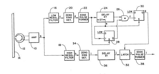
9 Referring to the drawings, and particularly to Fig. 1,
there is illustrated a dual channel read recovery system in
11 accordance with the presently preferred embodiment of the
12 present invention. The system includes an amplifier 10 having
13 an input from transducer 12 (which may be a magnetic read head)
14 which reads magnetic signals recorded on media 14. Amplifier
10 responds to transitions in the recorded signal to provide an
16 output (shown at waveform b in Fig. 2) to both the low
17 resolution filter 16 and high resolution filter 18. The low
18 resolution filter 16 is designed for frequencies at the low end
19 of the frequency range of the (1,7) code employed. Low
resolution filter 16 provides an output, waveform c in Fig. 2,
21 to zero crossing detector 20, which in turn provides an output,
22 waveform d in Fig. 2, to edge pulse former 22. Edge pulse
23 former 22 provides an output to delay circuit 24. Delay
24 circuit 24 will delay the signal received from pulse former 22
by a total of 4 clock periods and provide an input to AND gate
26 26. Delay circuit 24 is also center tapped to provide a
27 delayed signal, waveform e in Fig. 2, which is delayed two
28 clock cycles from the input from edge pulse former 22. The
29 waveform e in Fig. 2 is supplied to the overriding set input of
31 D-type flip-flop 28, whose D input is tied to a source of low
32 _ 5 _
1! ~.2~0a2~
Il . .
1¦¦ voltage. The Q-not output of flip-flop 28 is provided to a
Il ~econd input of AND gate 26. AND gate 26 Drovides a signal
31 output, shown as waveform f in Fig. 2, to the clock input of
4 D-type flip-flop 30. D-type flip-flop 30 has its D input
connected to a source of low voltage. The set input of
6 flip-flop 30 is connected to receive the waveform e shown in
7 Pig. 2. The Q output of flip-flop 30, shown at waveform g in
8 Fig. 2, is provided to latch 32.
g
In the high resolution channel, the output of the high
11 resolution filter 18 is shown at waveform h in Fig. 2, and is
12 ¦ provided to zero crossing detector 34, which in turn provides
14 an output, shown at waveform i in Fig. 2, to delay 36. Delay
15 ¦ 36 will delay the signal ~hown at waveform i by three clock
cycles, as shown at waveform j in Fig. 2. Latch 32 responds to
16 ¦ the signals shown at waveforms g and j in Fig. 2 to provide an
17 ¦ output shown at waveform k in Fig. 2 to edge pulse former 38,
18 ¦ which in turn provides an output, shown at waveform 1. Latch
¦ 32 is conditioned by a high input of waveform g to respond ~o
21 ¦ the edges of pulses of waveform j to provide the waveform k
I output.
2~ I
24 ¦ With reference to Fig. 2, the operation of the apyaratus
¦ ahown in Fig, 1 may be explained. Waveform a in Pig. 2 i8 a
25 ¦ representation of a string of binary digits and pulses
26 representative of each of the binary ones therein. Each pulse
28 is shown as having a positive going edge at the center of a
29 clock period T. The particular binary pattern illustrated at
waveform a illustrates both the high frequency (minimum number
31 o zeros) and low frequencies (maximum number of zeros) of a
3Z - 6 -
,1~
j~ ~.29~821
1 ¦ tl,7~ code. Thus, the waveform a comprises the binary bits
2 ¦ 1010101010000000100000001010101000000010. Waveform b
3 ¦ illustrates the signal provided by amplifier 10 which will vary
4 ¦ between positive and negative peaks in an analog fashio~. Low
5 ¦ resolution filter 16 responds to waveform b to provide a signal
6 ¦ shown at waveform c crudely converting peaks of waveform b to
7 ¦ zero cros~ings. However, the zero crossings of waveform c are
8 ¦ not perfectly aligned with the peaks of waveform b which
9 ¦ designate the centers of the transitions of waveform a. Thus,
10 ¦ the low resolution channel is not accurately tracking the
11 ¦ signal. Also noteworthy, waveform c displays an absence of
12 ¦ spurious signals caused by noise and the like. Zero crossing
13 ¦ detector 20 responds to the zero crossing of wavefor~ c to
14 provide waveform d, which is provided to edge pulse former 22,
which responds with short pulses for each edge of waveform d.
16 Pulse former 22 provides the pulse signal to the overriding set
17 input of flip-flop 28 to disable AND gate 26. Delay 24
18 provides a first delay signal to the clock input of flip-flop
19 28. The first delayed signal, shown at waveform e, is an exact
copy of the output of edge pulse former 22, except that it is
21 time delayed by two clock cycles. Thus, the successive edges
22 of waveform d provide separate pulses in waveform e, Note,
23 however, that because of the spacings, the trailing edge oF
24 pulse S0 in waveform d does not create a new pulse in waveform
e Thus, instead of four pulses for the four ones shown in
26 waveform a at the corresponding location, only three pulses are
27 generated by pulse former 22.
28
29 Delay circuit 24 operates two clock cycles (2T) following
the output of edge pulse former 22 to set the Q output of
321 _7_
lZ908Zl
~ 66082-283
l¦¦ flip-flop 30 high to provide a high wavefoem ~ output. At the
2 ¦¦ same time, the pulse on waveform e toggles flip-flop 28 to
3 ¦ force the Q-not output of flip-flop 28 high, thereby providing
4 an enabling input to AND gate 26. However, in the event
another pulse from pulse edge former 22 is received by the
6 overriding set input of flip-flop 28, the Q-not output of
7 flip-flop 28 is focced low to remove the enabling input to AND
8 gate 26. However, if no input pulse opera tes to set flip-flop
9 28, the Q-not output of flip-flop 28 remains high until a delay
oE an additional two clock cycles occurs (2T) and a second
11 delayed signal output occurs directly from delay circuit 24 to
12 AND gate 26. With both inputs of AND gate 26 now high, AND
13 gate 26 provides a pulse shown at waveform f in ~ig. 2 to the
~ clock input of flip-flop 30 to toggle the Q-output of flip-flop
low, as shown at waveform g.
16
17 It is evident, therefore, that the AND gate 26 will not be
lB operated to provide a pulse of waveform f unless there have
19 been four clock cycles of successive zeros~ Hence, edge 52 of
waveform d formed the pulse 54 of waveform f, thereby forcing
21 waveform g low as shown at edge 56.
22
23 The signal of waveform b from amplifier lO is also
24 provided to high resolution filter 18, which i8 shown at
waveform h in Fig. 2. The signal of waveform b is
26 characterized in that the peaks are accurately positioned in
27 zero crossovers of waveform h~ but is also characterized in
28 that the signal contains spurious signals, caused by noise and
29 the like The spurious signals form additional crossovers and
32 aks, such as at 58 in wavefoc h. Tùe signa of w~veform h
~ 908~i 66082 2~3
1¦¦ is provided to zero crossing detector 34 which provides a pulse
2il edge for each zero crossing of the signal of waveform h. Thus,
3 the signal of wavefo~m i is characterized by having pulse edges
4 at the zero crossings of waveform h matching the binary ones
shown in waveform a, and also by having additional zero
6 crossings 62 formed by the spurious signals 58 in waveform h.
7 Delay circu.it 36 delays the signal of waveform i.by a period of
time which is less than thè total period of time of the delay
9 of delay circuit 24. For the present purposes, we prefer that
the delay of delay circuit 36 delays signal i by three clock
11 cycles to form the signal of waveform j.
12
13 The signal of waveform j is provided as an input to latch
14 circuit 32. Latch 32 is responsive to the pulse edges of the
signal of waveform j to provide identical pulse edges in the
16 output waveform k, when the enable signal of waveform g is
17 high. When the enable signal of waveform g is low, as at 66 in
lB waveform 9, latch 32 will not respond to pulse edges in
19 waveform ;. As a result, since the low level of waveform g
occurs only during periods of lengthy successive zeros when
21 spurious signals are likely to occur in the high resolution
22 channel, the low levels of waveform 9 act to mask out the
spurious signal 64 of waveform j, resulting in waveform k.
24 Pulse edge Eormer 38 responds to the edges of the pulses of
signal waveform k to form the signal of waveform 1 to reproduce
26 the binary signal of waveform a.
27
28 The present invention thus provides a readback recovery
29 system in which long strings of absence of transitions are
3û detected by one of the channels to effectlvely disable the other
32 _ 9 _
1.2'30821
. ... .... . ..
1 channel from responding to and detecting spurious signals. As
2 a result, the low resolution channel may be designed to respond
3 to lower frequencies of the fre~uency range of the data
4 5i gnal.
6 Although the present invention described in connection
7 with detecting strings CL Lour or more zeros (absences of
8 transitions), the circuit can, o~ course, be adjusted to
9 respond to any number of zeros as desired~ merely by adjusting
the lengths of the delays 24 and 36. We prefer that the delay
11 of delay circuit 36 be somewhat shorter, such as one clock
12 cycle shorter, than the full delay of delay circuit 24. In
13 this respect, it is important that both channels be delayed so
14 that the detection circuits bring the two channels into
reasonable synchronism for operation in latch circuit 32.
16 However, for (1,7) codes the spurious signals will typically
17 occupy no more ~han about four clock cycles, usually commencing
18 during the third cycle of consecutive zeros and ending during
19 the sixth cycle of consecutive zeros, in the case of seven
consecutive zeros. Therefore, it is important that the signal
21 9 be low for at least about five clock cycles during these
22 periods ~y using the delays herein suggested, the appropriate
23 signal resolution is achieved, even with ordinary pulse drift
24 and inaccuracies of data recovery reflected in the signal of
waveform b. Due to the three clock cycle delay in the high
26 resolution channel formed by delay circuit 36, the spurious
27 signal 64 usually will not appear until about five clock cycles
28 (ih absolute time) following a transition 60 in waveform i or
29 transition 52 in waveform d. Since the waveform g goes low
31 about five absolute clock cycles following such transition, the
32 - 10 -
~ 908~1 66082-283
1 ¦ spurious signals are e~fectively blanked out by disabling the
2 ¦ high resolution channel during these periodsO Thus, recovery
3 ¦ of signals is possible, even of signals with long periods of no
4 transitions, such as in (1,7~ codes.
6 This invention is not to be limited by the embodiment
7 shown in the drawing and described in the description, which is
8 given by way of example and not of limitation, but only in
9 accordance with the scope of the appended claims.
11
12
13 7460G-4
16
17
li3
22
224
267
28
~9
31
32