Note: Descriptions are shown in the official language in which they were submitted.
2P~
CLOCK CI~CUIT SYNCHRONIZATION IN
DIGITAL TRANS~ISSION S~STE
Technical Field
This invention relates to clock circuits for
use in digital transmission systems and, ~ore
particularly, relates to circuit arrangements for
synchronizing local clock circuits at nodes in the
transmission system.
Background of the Invention
It is well recognized that it is desirable to
be able to transmit synchronously digital signals from
one node to another in a digital transmission system.
However, if the average rate of transmission of bits
from a node is not exactly equal to the average rate
incoming to the node, errors occur. Such errors are
defined as slips. A slip means that bits are
arbitrarily deleted if the input transmission rate
exceeds the output rate, or that bits are repeated or
inserted ar~itrarily if the input transmission rate is
slower than the output rate. To assure synchronization
and avoid slips, the nodes must be synchronized to a
common reference signal. To this end, each node
includes a local timing signal generator, commonly
referred to as a local clock, which generates timing
signals at a predetermined frequency. The local clock
is adjusted to be in synchronization with a reference
signal.
One known arrangement for realizing the
desired synchronization is described in U.S.
Patent 4,305,045. Disclosed are a frequency estimating
and synthesizing arrangement that includes a
programmable controller as part of a single phase lock
loop to control digitally an oscillator for obtaining
the desired synchronization of the local clock. A
o~
-- 2
problem arises with such arran~ements when the reference
timing signal link to the node failsO In such an event,
the digitally controlled oscillator is allowed to free
run at the long-term average frequency known at the node
at the time of the failure. Consequently, the free run
stability of the digitally controlled oscillator is of
critical importance in order to maintain performance
objectives. Such arrangements typically included
precision crystal oscillators which are controlled via a
digital-to-analog converter. In such oscillator
arrangements, all oE the circuitry is typically enclosed
in one or more oven chambers to provide a stable
temperature environment. Desirable features of such
arrangements include high digital control frequency
resolution and high stability, among others. These
features present conflicting design constraints which
are difficult to accommodate. Moreover, the high
stability constraint of such prior arrangement is
expensive to obtain.
Summary of the Invention
Problems associated with prior frequency
estimating and synthesizing arrangements are overcome,
in accordance with an aspect of the invention, by
separating the frequency estimatincJ and the frequency
synthesizing functions.
The frequency estimating is realized by
employing a phase-locked loop and a local high stability
fixed frequency oscillator to compute an estimate of the
frequency difference estimate between the received
reference timing signal frequency and the frequency of
the signal from the local fixed oscillator. Then, a
phase value corresponding to the frequency estimate
value is supplied to a frequency synthesizer including a
phase-locked oscillator to control a digitally
controlled oscillator for generating a signal having a
frequency which equals the algebraic sum of the fixed
frequency and the computed frequency difference.
~'~9~3~24
-- 3
i~hen the reference timing signal is lost
and/or a phase error is too great, the last generated
frequency difference estimate value is retained at a
constant value and continuously supplied to the phase-
locked oscillator. Consequently, the phase-locked
oscillator is never allowed to free run, thereby
yielding an output with a stability equal to the fixed
frequency oscillator without the need for an extremely
stable digitally controlled oscillator.
More specifically, the frequency estimating is
realized, in accordance with an aspect of the invention,
by sampling an incoming reference timing signal with the
output signal from a fixed oscillator to obtain a
sampled input phase signal and employing a phase-locked
loopO The phase-locked loop includes an algebraic
difference circuit for generating a phase error signal
which is the difference between the sampled input phase
signal and a local phase signal. Then, a loop
compensation filter is supplied with the phase error
signal to generate an estimate of a frequency difference
between the incoming reference timing signal frequency
and the oscillator output signal frequency. The
estimate signal is integrated, in accordance with
another aspect of the invention, to generate the local
phase signal. The local phase signal is phase-locked to
the incoming reference timing signal.
An output timing signal is generated, in
accordance with another aspect of the invention, by
supplying the local phase signal to a second phase-
locked loop. The second phase-locked loop includes a
di~itally controlled oscillator which i9 controlled by a
frequency control signal to generate the output timing
signal. A sampled output phase signal is generated by
sampling the output timing signal with the output from
the fixed oscillator. A second phase error signal is
generated by obtaining the algebraic difference of the
local phase signal from the frequency estimator and the
- 4 -
sampled output phase signal. The second phase error
signal is supplied to a second loop compensation filter
which generates the frequency control signal for
controlling the frequency of the digitally controlled
oscillator.
In one specific embodiment of the invention, a
single processor is employed in conjunction with a fixed
oscillator, two phase samplers and a digitally
controlled oscillator to realize both the phase-locked
loop which generates the frequency difference estimate
value and the phase-locked oscillator which generates
the desired output timing signal.
In another embodiment of the invention, first
and second frequency estimators are employed for
generating first and second frequency difference
estimates ~etween first and second received reference
timing signals, respectively, and the frequency of the
local fi~ed oscillator signal. ~ selector is employed
to select one of the frequency estimates in accordance
2~ with predetermined criteria~ The selected estimate is
then integrated to obtain a corresponding phase value
; which is supplied to the frequency synthesizer phase-
locked oscillator. The frequency synthesizer includes
in the phase-locked loop a digitally controlled
oscillator that generates the desired synchronization
signal. If one of the incoming reference timing signals
is lost and/or the associated phase error is too great,
the frequency estimate generated from the other
reference timing signal is selected. If ~oth of the
reference timing signals are lost and/or the associated
phase errors are too great, the frequency estimate ~rom
the last non-lost reference timing signal is selected
having an assoclated phase error within prescribed
limits.
~ 3~
- 4a -
In accordance with one aspect of the invention there
is provided an apparatus for generating an estimate of the
frequency of an incoming reference timing signal comprising:
an oscillator for generating an output signal (Ts) having a
fixed frequenc~l and corresponding period; means for generating
a sampled input phase signal (~j(n)~ by sampling the phase of
said incoming reference timing signal (phij(t)) with said
oscillator output signal (Ts); a first digital phase-locked
loop including first combining means for algebraically
combining said sampled input phase signal with a local phase
signal (PHLOC(n)) to obtain a first phase error signal
(PHEI(n)) which is the algebraic difference between said
sampled input phase signal and said local phase signal, first
loop compensation filter means supplied with said first phase
error signal for generating an estimate signal (FRQEST(n))
representative of a frequency difference between said incoming
reference timing signal frequency and said oscillator output
signal frequency, and integrator means supplied with said
estimate signal for generating said local phase signal,
wherein said local phase signal is phase-locked to said
incoming reference timing signal.
In accordance with another aspect of the invention
there is provided an apparatus for generating an output timing
signal comprising: an oscillator for generating an output
signal having fixed frequency and corresponding period; means
for generating a sampled input phase signal by sampling the
phase of an incoming reference timing signal with said
oscillator output signal; a first digital phase-locked loop
including means for algebraically combining said sampled input
phase signal with a local phase si.gnal to obtain a first phase
error signal which is the algebraic difference between said
sampled input phase signal and said local phase signal, first
loop compensation filter means supplied with said first phase
error signal for generating an estimate signal representative
of a frequency difference between said incoming reference
timing signal frequency and said oscillator output signal
frequency, and integrator means supplied with said estimate
8~
- 4b -
signal for generating said local phase signal, wherein said
local phase signal is phase-locked to said incoming reference
timing signal; and a second digital phase-locked loop
including a digitally controlled oscillator responsive to a
frequency control signal (F~QCTL(n)) for generating a output
timing signal (Qo(t))r generating means for generating a
sampled output phase signal (PHOUT(n)) by sampling the phase
of said output timing signal with said oscillator output
signal (TS), second combining means for algebraically
combining said sampled output phase signal (PHOUT(n)) with
said local phase signal (PHLOL(n)) to obtain a second phase
error signal (PHE2(n)) which is the algebraic difference
between said local phase signal and said sampled output phase
signal, second loop compensation filter means supplied with
said second phase error signal for generating said frequency
control signal, wherein said output timing signal is phase-
locked to said local phase signal.
~.29(~
,
Brief _escription of the Drawing
In the Drawing:
FIG. 1 shows in simplified block diagram form
an embodiment of the invention;
~IG. 2 depicts in simplified block diagram
form another embodiment of the invention;
FIG. 3 shows in simplified block diagram form
details of the digitally controlled oscillator (DC~)
used in FIGs. 1, 2, 6 and 7;
FIG. 4 depicts in simplified form details of
; the phase sampler and counter employed in FIGs. 1, 2, 6
and 7;
FIG. 5 is a flow chart illustrdting the steps
for operation of the embodiment of FIG. 2;
; 15 FIG. 6 shows in simplified block diagram form
an embodiment of the invention including redundant
frequency estimators;
FIG. 7 depicts in simplified form details of
another embodiment of the invention including redundant
freq~ency estimators; and
FIGs. 8, 9 and 10 form a flow chart
illustrating the steps for operation of the embodiment
of FIG. 7.
Detailed Description
FIG. 1 shows in simplified block diayram form
a synchronization arrangement including an embodiment of
the invention. In accordance with an aspect of the
invention, instead of employing high precision digitally
controlled variable frequency oscillators of the prior
art which required expensive temperature compensation
ovens and the like, a simpler precision fixed oscillator
i5 employed as a local frequency reference in
conjunction with a digital phase-locked loop to obtain a
signal representation of the frequency oE an incoming
reference timing signal relative to the local oscillator
frequency reference. Additionally, the local frequency
reference is employed in conjunction with another
phase-locked loop to synthesize a signal using "low"
quality, as compared to the prior high precision
variable oscillators, so that the frequency oE the
synthesized signal is identical to a long-term average
of a desired timing signal reference. Consequently, if
the incoming reference timing signal is lost, the
stability of the frequency of the synthesized timing
signal is related essentially to the sta~ility of the
local fixed oscillator. The decoupling of the
estimation and synthesis functions allows treatment of
each on an individual basis and relaxes design
cor)straints. This results in the use oE a lower cost
Eixed precision oscillator and variable frequency
oscillator as compared to the higher cost precision
variable frequency oscillators used heretoforeO
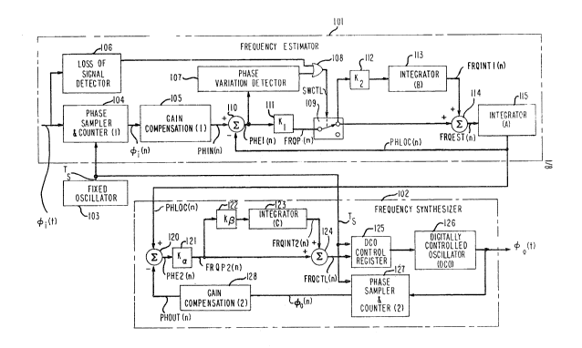
Accordingly, shown in FIG. 1 are frequency
estimator 101, frequency synthesizer 102 and fixed
precision oscillator 103. Frequency estimator 101
includes phase sampler and counter (1) 10~, gain
; 20 compensation circuit 105 and a controllable phase-locked
loop. ~dditionally, included are loss of signal
detector 106, phase variation detector 107, OR gate 108
and controllable switch 109. The phase-locked loop is,
in this example, a so-called second order proportional-
plus integral control type. The phase-locked loop
includes summer 110, proportional gain unit (Kl) 111,
integral gain unit (K2) 112, integrator (B) 113,
summer 114 and integrator (~) 115. Proportional gain
unit (Kl) 111, integral gain unit (K2) 112,
integrator (B) 113 and summer 114 form a so-called loop
compensation filter.
~ n the Eollowing description, it will be
apparent to those skilled in the art that the digital
modules employed in both ~requency estimator 101 and
frequency synthesi~er 102 are being clocked via Ts (not
specifical]y shown).
~90~
-- 7 --
Details of sampler and counter (1) 104 are
shown in FIG. 4. Accordingly, shown are counter 401,
D-type flip-flop 402 and latch memory 403. The incoming
timing signal ~i(t) is supplied to counter 401 and, via
in~erter 404, to the clock input (CLK) of flip-flop 402,
Counter 401 is, in this example, a modulo-kl counter.
The value of kl is determined as
kl = closest inteyer of [fi Ts] (1)
where fi is the nominal frequency of the incoming timing
link signal, for example, 1.54A MHz for domestic systems
or 2.043 M~12 :Eor European systems, and Ts is the
sampling interval of the output from fixed
oscillator 103, in this example, 1 millisecond. In this
: example, oscillator 103 has a precision of one part in
101 per day. The local clock signal having period Ts
from fixed oscillator 103 (FIG. 1) is supplied to the
D input of flip-flop 402. The Q output of flip-flop 402
is supplied to control latch memory 403. The output of
counter ~01 is supplied to latch memory 403. ~he count
value in counter 401 is sampled and stored in latch
~ memory 403 at every time interval TS in response to the
; Q output of flip-flop 402. Flip-flop 402 is included to
insure that the output of counter 401 is stable before
~ storing its ~alue in latch memory 403- The output 0i(n)
; 25 from latch memory 403 is supplied to gain compensation
unit 105. Phase sampler and counter 104 generates
: output ~i(n) which is a sampled representation of the
continuous time si~nal ~i(t) at sampling interval Ts
generated by fixed oscillator 103. It is noted that (n)
indicates the nt~ sample at the nT5 sampling interval.
Returning to EIG. 1, the output from phase
sampler and counter (1) 104, ~i(n), is supplied to gain
compensation unit 105. As indicated above, the
characteristics of phase sampler and counter (1) 104 are
such that kl steps represent one cycle of the output
~ 2~
signal 0i(n). The value kl depends on the sampling
rate, Ts, and on the input signal frequency, fi.
Accordingly, phase sampler and counter (1) 104 provides
a "gain" factor
Kpsl = N (2)
where N is the nurnber of bits at the o~tput of latch
memory 403 (FIG. 4) and kl is the modulo of phase
sampler and counter(l) 104. This gain factor Kpsl is
; nulled out by gain compensation unit 105. Therefore,
the output Erom gain compensation unit 105, which is the
input to the phase-locked loop of frequency
estimator 101, is
PHIN(n) = ~ ~i(n) (3)
The phase-locked loop employed in frequency
estimator 101 is a so-called second order proportional-
plus integral control type where Kl is the proportional
gain and K2 is the integral gain. The proportional gain
term Kl produces short term frequency variations
required to minimi~e the phase error. The integral gain
term K2 represents a long term frequency average equal
to the integrator (A) 115 input to obtain frequency
lock. Accordingly, the incoming phase signal PHIN(n) is
supplied to a first input of summer 110 while the local
phase signal PHLOC from integrator (A) 115 is supplied
to a second input oE summer 110. Summer 110 generates
the algebraic difference of the supplied signals,
namely,
PHEl(n) = P~IIN(n) - PHLOC(n) (4)
which represents the phase error to be corrected and
thereby achieving phase-lock in the loop. The phase
~ ~9q~
difference error P~lEl(n) is supplied to proportional
gain (Kl) unit 111 which generates the proportional
: frequency term FRQPl(n), namely,
FRQPl(n) = Kl PHEl(n). (5)
The proportional frequency term FRQPl~n) from
Kl gain unit 111 is supplied via controllable switch 109
to K2 gain unit 112 and a first input of summer 11~.
T~le output of K2 gain unit 112 is supplied to
integrator (B) 113 which, in turn, generates integral
frequency term E`RQINTl(n) and supplies the same to a
second input of summer 11~. Integrator (B) 113 updates
the integral frequency term FRQIN~rl(n) as follows:
FRQINTl(n~ FRQPl(n) K2) ~ FRQINTl(n). (6)
Summer 11~ generates the desired frequency estimate,
namely,
; FPQEST(n) = FRQPl(n) + FRQINTl(n). (7)
The frequency estimate output from summer 114
: is supplied to integrator (A) 115 which generates the
phase-lock signal PHLOC(n). PHLOC(n) is updated in
integrator (A) 115 as follows:
PHLOC(n-~l) = FRQEST(n) + PHLOC(n). (~)
The use of integrator (A) 115 effectively
decouples the frequency estimation process from the
frequency synthesis process, in accordance with an
aspect o:E the invention. The decoupling is rea:lized
because integxator (A) 115 is a digital model of a
voltage-controlled oscillator that normally would be
used in a phase-locked loop to generate the local phase
signal PllLOC(n) substantially equal to input phase
signal PHIN(n). It is important to note that the output
8~4
. ~
-- 1.0 --
of integrator (A~ 115 is a value represented in digital
form. It is also desirable that the frequency
estimate FRQEST generated by frequency estimator 101
should have higher resolution than kl steps in order to
reduce the quantization noise.
Also important to the invention is inhibiting
changes to the frequency es-timate input, namely, FRQEST,
of integrator (~) 115. This inhibiting is realized, in
accordance with an aspect oE the invention, by employing
controllable switch 109 effectively to cause a zero
value input to be supplied directly to the first input
of summer 11~ anc3, via K2 gain unit 112 and
integrator (B) 113, to the second input of summer 114
when either there is a loss of the incoming timing
signal ~i(t) or too large a phase variation in the phase
error signal P~3El(n). The amount and type of phase
variation is system-dependent and, consequently, will be
different for each particular application. In one
example, any phase error greater than 10 microseconds of
phase is unacceptableO Switch 109 is controlled by an
output from OR gate 108. Consequently, loss of signal
detector 106 supplies a control signal to a first input
of OR gate 108 indicative of whether incoming timing
signal ~i(t) is present or not. ~ logical 1 indicates
that 0i(t) is lost.
Similarly, an output from phase variation
detector 107 is supplied to OR gate 108 indicative of
whether the phase error PHEl~n) is too large or not. A
logical 1 signal indicates that Pl-lEl~n~ is outside
prescribed limits (10 microseconds in this example).
Controlla~le sw~tch 109 is responsive to the logical 1
signal Erom OR gate 108 to open-circuit the circuit
connection between gain unit 111 and gain unit 112 and
summer 114 when either loss of incoming timing
sigr~al ~i~t) is detected or a variation in the phase
value of PHEl~n) greater than a predetermined threshold
is detected. Opening of controllable switch 109
9~8~L
-- 11 --
inhibits updating of integrator (B) 113 and
integrator (A) 115. That is to say, a zero value signal
is supplied to integrator (B) 113 and to the first inpu-t
of summer 114. Consequently, the frequency
estimate FRQEST(n) remains constant at its long-term
average value, in accordance with an aspect of the
invention, and integrator (A) 115 continues to integrate
FRQEST(a) in accordance with equation (8) at in~erval Ts
to generate PllLOC(n). Thus, P~lLOC(n) continues to have
a constant rate of change as though frequency
estimator 101 was still in phase-lock with the incoming
reference timing signal ~i(t).
The local phase signal Pl-lLOC(n) from frequency
estimator 101 is supplied to frequency synthesizer 102
which also includes a phase-loc~ed loop. Incluc~ed in
the frequency synthesizer 102 phase-locked loop are
summer ~20, Kq gain unit 121, K~ gain unit 122,
integrator (C) 123, summer 124, sampler 125, digitally
controlled oscillator 126, phase sampler and
counter (2) 127 and gain co~pensation unit 128. K~ gain
unit 121, K~ gain unit 122, integrator (C) 123 and
sum-mer 124 ~for~n a so-called loop compensation filter.
The output PHLOC(n) from frequency
estimator 101 is supplied to a first input of summer 120
in frequency synthesizer 102. The gain compensated
output PI~OUT(n) from gain compensation unit 128 is
supplied to a second input of summer 120. Summer 120
yields the algebraic difference signal PHE2(n), where
PHE2(n) = PHLOC(n) - PHOUT(n). (9)
The output from summer 120 is supplied to
proportional gain 1~ unit 121. Gain unit 121 generates
FRQP2(n) = K~ PHE2(n). (10)
In turn, the output FRQP2(n) fro~ K~ gain unit 121 is
, . :
~9~8Z~
- l2 -
supplied to a first input of summer 124 and to integral
gain K unit 122. The output from K~ gain unit 122 is
suppli~ed to integrator (C) 123. The integrated output
from integrator (C) 123 is supplied to a second input of
summer 124. Integrator (C) 123 updates the integral
frequency term FRQINT2(n) as follows:
FRQINT2(n~ (FRQP2(n) K~) + FRQINT2(n). (lL)
Summer 124 generates the desired sampled frequency
control signal
FRQCTL(n) = FRQP2(n) ~ FRQCTL(n). (12)
The frequency control signal FRQCTL(n) is
latched in DCO control register 125 at each interval T
Register 125 holds the value of FRQCTL(n) constant
during the local sampling interval Ts The latched
value of FRQCTL(n) is supplied to digitally controlled
oscillator (DCO) 126 which generates the desired output
timing signal 0O(t).
Details of DCO 126 are shown in simplified
form in FIG. 3. Accordingly, shown are digital-to-
analog (D/A) converter 301 and voltage-controlled
oscillator 302 which operate in well-known fashion to
generate the desired output timing signal ~o(t) It
should be noted, however, that the precision of VCO 302
can be much lower than prior VCO's used in the prior
single phase-locked loop frequency synthesizer
arrangernents. This is because of the fact that the
frequency estimator L01 output is held constant when the
incoming timing signal is lost and, therefore, frequency
synthesizer 102 is always in phase-lock and never free
runs. Because prior VCO's were allowed to free run when
the incoming timing signal was lost, they were required
to have extremely stable frequency characteristics when
the input control signal was constant.
2~
Returning to FIG. 1, the output timing
signal 00(t) is supplied to phase sampler and
counter(2) 127 which generates a sampled signal ~O(n).
Phase sampler and counter(2) 127 is essentially
identical to phase sampler and counter(l) 10~ as shown
in FIG. ~. Accordingly, 00(n) is generated in the same
fashion as 0i(n) described above. The only difference
is that
k2 = closest integer of [fO Ts]. (13)
It is noted that
fo = kl fi (1~)
where fO is the frequency of output signal 00(t) and fi
is the frequency of input signal ~i(t). The output from
phase sampler and counter(2) 127, ~O~n), is gain
; 15 compensated via gain compensation unit 128 to yield
PHO~T(n). Gain compensation unit 128 is essentially
identical to unit 105 and nulls out the phase sampler
gain, namely, KpS2 = 2, to generate
PH~UT(n) = ~ ~o(n) (15)
It is noted that when the input FRQEST(n) to
integrator (A) 115 of frequency estimator 101 is held
constant, the DCO 126 in frequency synthesizer 102 is
not allowed to free run and the phase-locked loop
remains in phase-lock with PHLOC(n). The frequency
stabi.lity of output 00(t) is then dependent on the
stability of Eixed oscillator 103 and the number of bits
sed to represent the frequency estimate input FRQEST(n)
to integrator (~) 115 ~n prior arrangements, the
number oE bits that could be used to represent ~RQEST(n)
was limited because a digital-to-analog (D/A) converter
was required for use with a VCO. The more bits used in
~ ~9(3~'~4
_ 14 -
such D/A converters increased their cost.
FIG. 2 shows a processor-implemented
embodiment of the invention corresponding to the
embodiment of FIG. 1. Accordingly, shown are phase
sampler and counter 201, phase sampler and counter 202,
fixed precision oscillator 203, processor 204 and
digitally controlled oscillator (DCO) 205.
Processor 204 includes a microcomputer arrangement of a
type known in the art. In this example, an Intel 80l86
is used. The incoming reference timing signal, 0i(t),
is s~lpplied to phase sampler and counter 201 which, in
response to the local timing signal having period TS
from fixed oscillator 203, generates the sampled timing
signal 0i(n). Similarly, phase sampler and counter 202
is supplied with the output timing signal 0O(t) from
DCO 205 to generate a sampled output signal ~O(n) in
response to the local timing signal from fixed
oscillator 203. The sampled incoming timing
signal 0i(n) and sa~pled output timing signal ~O(n) are
supplied to processor 204. Phase sampler and counter
circuits 201 and 202 are identical to that shown in
FIG. 4 and described above. Also supplied to
processor 204 is the local timing signal from fixed
oscillator 203 which interrupts the processor at
period ~s Processor 204 generates the frequency
control signal FRQCTL(n) which is stored in a register
of the processor 204 and supplied to DCO 205.
Operation of processor 204 in generating the
frequency control signal FRQCTL(n) is shown in the flow
chart of FtG. 5. Accordingly, the program routine is
entered upon each interrupt generated at period Ts via
501. I'hereafter, conditional branch point 502 tests to
determine whether incomin~ timiny signal ~i(t) is
present. If the test result in step 502 is YES,
operational block 503 causes phase sampler and
counter (1) 201 to be read. This supplies ~i(n) to the
processor 204. Then, operational block 504 causes
8~
-- 15 --
PHIN(n) to be computed. This is achieved by gain
compensating ~i(n) as described in equation (3) above.
Operational block 505 causes the computation of the
phase error 1 signal, PltEl(n), in accordance with
equation (4) above. Conditional branch point 506 tests
to determine that the phase error PHEl(n) is within
predetermined limits. If the tes~ result in step 506 is
YES, operational block 507 causes the computation of
proportional frequency term FRQPl(n), in accordance with
equation (5) above. Then, operational block 509 causes
the computation oE integral frequency term FRQIN'rl(n),
in accordance with equation (6) above. Thereafter r
operational block 509 causes the computation of the
desired frequency estimate, FRQEST(n), in accordance
with equation (7) above.
Returning to step 502, if the test result is
NO indicating that the incoming timing signal ~i(t) has
been lost, control is transferred to operational
block 510 which causes the proportional frequency term
FRQPl(n) to be set to zero. Similarly, if the test
result in step 506 is NO indicating the phase error 1,
PHEl(n), is too great, control is transferred to
operational block 510 which causes the proportional
frequency term FRQPl(n) to be set to zero. This is
equivalent to opening switch 109 of FIG. 1 which
inhibits updating of integrator (B) 113 (FIG. 1). Then,
operational block 508 causes the integral frequency term
FRQINTl(n) to be computed, in accordance with
equation (6) above. Thereafter, operational block 509
causes the computation of the frequency estimate,
FRQEST(n), in accordance with equation (7) above. As
indicated above, when the proportional Erequency term
FR;;?Pl(n) i5 set to zero, the resulting frequency
estimate, FRQE5'r(n), remains constant.
Operational block 512 causes the phase sampler
and counter (2) 202 to be read which supplies the
sampled version of the output signal ~O(n) to
~ X:9~
- 16 -
processor 204 (FIG. 2). Operational block 513 causes
computation of the phase error 2, P~E2(n), signal by
gain compensating the sampled output signal ~O(n) as
described in equation (9) above. Operational block 514
causes computation of proportional frequency term
FRQP2(n), in accordance with equation (10) a~ove. Then,
operational block 515 causes integral frequency term
FRQINT2tn), to be computed in accordance with
equation (11) above. Operational block 516 causes
computation of the DCO 205 control signal, FRQCTL(n), in
accordance with equation (12). Then, operational
block 517 causes the DCO control signal, FRQCTL(n), to
be written in a DCO control register which, in turn,
supplies FRQCTL(n) to DCO 205 (FIG. 2) for generating
the output timing signal ~o(t)~ Operational block 518
causes the updated local phase signal PElLOC(n+l) to be
computed in accordance with equation ~8). Operational
block 519 causes the updated integral frequency term
FRQINTl(n+l) to be computed in accordance with
equation (6). Operational block 520 causes the updated
integral frequency term FRQINT2(n+1) to be co~puted in
accordance with equation (11). Control is thereafter
returned to some other process via 521 until the next
interrupt causes re-entering of this routine.
FIG. 6 shows in simplified block diagram form
details of a redundant synchronization circuit with
multiple timing reference signals, in accordance with an
aspect of the invention. Accordingly, shown are
Erequency estimator (A) 601, frequency
30 estimator (B) 602, selector 603, integrator (D) 60~,
frequency synthesizer 605 and Eixed oscillator 606~
First and second incoming timing signals ~iA(t) and
~(t) and the local timing signal having period Ts from
fixed oscillator 606 are supplied to frequency
35 estimators 601 and 602, respectively. The output from
oscillator 606 is also supplied to integrator 60~ and
frequency synthesizer 605. Frequency estimators 601 and
~ ~29~ 4
- 17 -
602 are essentlally identical to frequency estimator 101
of FIG. 1 except that the frequency estimate signal,
FXQEST(n)(A), and switch control signal, SWCTL(A), from
estimator 6~1 and frequency estimate signal,
FRQEST(n)(B), and switch control signal, SWCTL (B), from
estimator 602 are supplied to selector 603.
Selector 603 includes logic responsive to the switch
control signals 5WCTL(A) and S~CTL(B) for controllably
selecting one of frequency estimate signals FRQEST(A) or
FRQEST5B) to integrator (D) 60~. The selection process
is, if both S~CTL(A) and SWCTL(B) are Ealse, i.e.,
representative of a logical 0, indicating both incoming
timing signals 0iA~t) and 0iB(t) are present and that
the corresponding phase errors PHEl(n)(A) and P~El(n) (B)
are within prescribed limits, then FRQEST~) is
selected. If either one of SWCTL (A) or SWCTL (B) is
true, i.e., representative of a logical 1, indicating
that the corresponding incoming timing signal is lost or
that the corresponding phase error is outside the
prescribed limits, the other one of frequency estimates
FRQEST(n)(A) or FRQEST(n) (B) is selected. If both
SWCTL(A) and SWCTL(B) are true, indicating that either
both the timing signals 0iA~t) and ~iB(t) are lost or
both the corresponding phase errors are out of limits or
any combination thereof, the frequency estimate signal
is selected corresponding to the last incoming timing
signal which was present having a phase error within the
prescribed limits.
The selected frequency estimate, FRQEST(n)(S),
is supplied to integrator (D) 60~. Integrator (D) 60
is identical to integrator (A) 115 of FIG. 1 and
generates the selected local phase signal PHLOC(n)(S) in
accordance with equation (8) above. The reason Eor
employing the additional integrator (D) 60~ is to avoid
phase discontinuities tnat would result in the timing
output 9ignal 00(t) by switching the local phase signals
PHLOC(n)(A) and PllLOC(n) (B) generated in frequency
- 18 -
estimators 601 and 602, respectively. These
discontinuities are avoided by supplying the frequency
estimate signals FRQEST tn) (A) and FRQEST (n)(B) to
selector 603 for switching and, then, integrating after
the selection to obtain PHLOC(n)(S).
The local phase signal PHLOC(n)(S) is supplied
to frequency synthesizer 505 which generates the output
timing signal ~o(t)~ Frequency synthesizer 605 is
identical to frequency synthesizer 102 of FIG. 1 and
described ahove.
FIG. 7 shows in simplified block diagram form
another embodiment of a redundant timing synchronization
eircuit, in aecordance with an aspect of the invention.
Aeeordingly, shown are phase sampler and
counter (A) 701, phase sampler and eounter (B) 702,
fixed oscillator 703, processor 704, digitally
controlled oseillator 705 and phase sampler and
counter (C) 706. Proeessor 704 includes a
microcomputer, for example, an Intel 8018~. Phase
sa~pler and eounter circuits 701 and 702 are identical
to phase sampler and counter 104 of FIG. 1 and described
above. Similarly, phase sampler and counter 706 is
identical to phase sampler and counter 127 of FIG. 1 and
described above. Fixed oscillator 703 is identical to
fixed oseillator 103 of FIG. 1 and DCO 705 is identical
to DCO 126 of FIG. 1 and described above. Incoming
timing signals 0iA(t) and 0iB(t) are supplied to phase
sampler and counter (A) 701 and phase sampler and
eounter ~B) 702, respectively. Phase sampler and
eounter (A) 70l and phase sampler and eounter (B) 702,
in response to the fixed oscillator 703 output of
period Ts~ generate sampled versions of the ineoming
timing signals, namely, 0iA(n) and 0ia(n), respectively.
Similarly, phase sampler and eounter(C) 70~ generates,
; 35 in response to the Eixed oscillator output signal, a
sampled version of the output timing signal ~o(t)~
namely, 0O(n). These sampled signals, 0i~(n), 0iB(n)
~ , ., ~ .
8~
,. -- 19 --
and ~O(n), along with the fixed oscillator 703 output,
are supplied to processor 7n4. Processor 704 is a
microcomputer system havin~ a program stored therein to
effect the dual frequency estimation functions, the
frequency esti~ate selection function, integration of
the selected frequency estimate and generation of the
DCO control signal, namely, FRQCTL(n). The output of a
DCO control register in processor 704, namely,
FRQCTL(n), is supplied to DCO 705 which, in turn,
generates the output timing signal ~o(t).
FIGs. 8, 9 and l0 when connected AA-AA and
~-BB form a flow chart of the steps of a program
routine performed by processor 704 in generating
DCO control signal FRQCTL(n) for controlling DCO 705 to
generate the output timing signal 00(t). Accordingly,
the program routine is entered via 801 in response to an
interrupt caused by the fixed oscillator 703 output of
period Ts. Thereafter, operational block 802 initially
sets timing link (A) status to a logical 0. This
initially indicates that the signal 0iA(t) is present
and not lost. Conditional branch point 803 tests to
determine if incoming timing si9nal ~iA(t) is present.
If the test result in step 803 is YES, operational
block 804 causes phase sampler and counter (A) 701 to be
read. This supplies the sampled version ~iA(n) of the
incoming timing signal ~iA(t) to processor 704. Then,
operational block 805 causes the computation of the
phase in (A), PHIN(n)(A), which is the gain compensated
version of ~iA(n), in accordance with equation (3)
above. Operational block 806 causes the computational
of the phase error (A), P~IEl(n)(A), in accordance with
equation (4) above. Conditional branch point 807 tests
to determine iE the phase error is within prescLibed
limits set Eor the particular system. IE the test
result in step 807 is YES, operational block 808 causes
the computation of the proportional frequency
term (A) FRQP(n)(A), in accordance with equation (5)
1 29~
_ 20 -
above~ Thereafter, operational block 811 causes the
computation of integral frequency term (A) FRQINT(n)(A),
in accordance with equation (6) above.
Returning to conditional branch point 803, if
the test result is NO, the timing signal 0i~(t) is lost
and control is transferred to operational block 809.
Similarly, if the test result in conditional branch
point 807 is NO, the phase error is out of limits and
control is transferred to operational bloclc 809.
Operational block 809 sets the incoming timing link (A)
status to be a logical 1 indicating that the frequency
estimate being gererated in response to the incoming
timing link signal 0iA(t) should not be updated. To
this end, operational block 810 sets the proportional
frequency term (A) FRQP(n)(A) = 0. This is essentially
the same as opening switch 109 in FIG. 1. Thereafter,
operational block 811 causes the computation of the
integral frequency term (A) FRQINTl(n)(A), also in
accordance with equation (6) above.
Operational block 812 causes the computation
of frequency estimate (A), FRQEST(n)~A), in accordance
with equation (7) above.
Operational block 813 causes the updated local
phase PHLOC(ntl)(A) to be computed in accordance with
equation (8) above.
Operational block 814 causes the updated
integral frequency term FRQINTl(n-~l)(A) to be computed
in accordance with equation (6). This completes the
steps in generating the frequency estimate (A),
FRQEST(n)(A).
Steps 816 through 828 are identical to
steps 801 through 81~, respectively, except they effect
the generation of frequency estimate (B) for incoming
timing signal ~iB(t). Accordingly, steps 816 through
828 will not be described again in detail.
o~
- 21 -
Conditional branch point 830 tests the timing
link status (A) and the timing link status (B) to
determine if both incoming timing signals ~iA(t~ and
~iB(t) are present. If the test result is Y~S,
operational block 831 causes the frequency estimate (A),
FRQEST(n)(A), to be selected for use in generating the
desired output timing signal 00(t) and control is
transferred to operational block 832. If the test
result in step 830 is N0, conditional branch point 833
tests the timing link status (A) to determine iE it is a
logical 0, in~icating that 0iA(t) is present and that
the corresponding phase error (A) is within limits. If
the test result in step 833 is YES, operational
block 831 causes selection of frequency estimate (A),
FRQEST(n)(A), and control is transferred to operational
block 832. If the test result in step 833 is N0, i.e.,
timing link status (A) is a logical 1, indicating that
~ (t) is not present or that the corresponding phase
error (A) is not within limits, conditional branch
point 834 tests the timing link status (B) to determine
if timing link signal ~iB(t) is present and that the
corresponding phase error (B) is within limits. If the
test result in step 834 is YES, operational block 835
causes the selection of frequency estimate (B),
FRQEST(n)(B). Thereafter, control is tLansferred to
operational block 832. If the test result in step 834
is N0, i.e., the timing link status (B) is a logical 1,
indicating that ~ig(t) is not present or that the
corresponding phase error (B) is not within limits,
operational block 836 causes the selection of the last
one of requency estimate (A), ~RQEST(n)(A), or
frequency estimate (B), FRQEST(n)(B), that the
orresponding timing link status was a logical 0. That
i5 to say, the frequency estimate is selected for the
last timing link that indicated that the corresponding
incoming timing signal was present and the corresponding
phase error was within li~its prior to the timing link
9(~
- 22 -
status becoming a logical 1. Thereafter, control is
transferred to operational block 832.
Operational block 832 causes the selected
frequency estimate value to be integrated to obtain the
local phase value, PHLOC(n)(S). The integration is the
same as performed by integrator (D) 604 of FIG. 6 in
accordance with equation (8) above.
Operational block 837 causes phase sampler and
counter (C) to be read.
Operational block 838 causes the computation
of the phase error (2), PHE2(n), in accordance with
equation (9) above.
Operational block 839 causes the computation
of the proportional frequency terln FRQP2(n), in
accordance with equation (10) above.
Operational block 840 causes the computation
of integral frequency ter,n FRQI~T2(n), in accordance
with equation (11) above.
Operational block 841 causes the computation
of the DCO frequency control signal, FRQCTL(n), in
accordance with equation (12) above.
Operational block 842 causes the DCO frequency
control signal, FRQCTL(n), to be written into a register
which stores the frequency control signal until it is
updated. The frequency control signal, FRQCTL(n), is
supplied to DCO 705 (FIG. 7).
Operational block 843 causes the updated local
phase signal PHLOC(n+l)(S) to be computed in accordance
with equation (8) for PHLOC(n~l).
Operational block 844 causes the updated
integral frequency term FRQIN~I'2(n~1) to be computed in
accordance with equation (11).
Thereafter, the control is returned to a main
process via 845 until the next interrupt is received
from fixed oscillator 703.