Note: Descriptions are shown in the official language in which they were submitted.
' ~ e
l FIELD OF T~E IN~ENTION
-
The present invention relates to ~ic~ocoded machlnes
~'~micro-machi~es"), and more particularly to micro-machines ~hich
run aæynchronous from the system in which they are interiaced.
5 ~ACKGROUND 0~ THE INVE~TION
In prior art computer systems employing micro-machines which
are c~ocked asynchronously from the system with which they are
inter~ace~ (i.e. wherein the clock o~ the mlcro-machine ls out o~
phase ~,r~has a different period than the clock running the system
~ith which the mlcro-machine is interXaced), latency (the time
lag bet;ween the time o~ issuance o~ an incoming instruction to
the micro-machine and the time of instruction completion) is a
crit~cal and troublesome problem. For purposes o~ the
Specification herein, the term "micro-machine" or asynchro~ous
micro-~achine is de~ined as a computational computer system which
includes a command or instruction register which is typically
up~ d at every clock cycle with commands that are read i'rom a
microstore memory and which are used to execute an incoming
i-nstruction. These commands typically are comprised of controls
~ign~ls as well as data.
In order to overcome the problem of latenc~ which occurs i~
micro-machines that run asynchronously from the CPU from ~hich
the mi~ro~machine receives its instructions, prior art systems
employ various synchronization interfacing circuitry between the
master CPU and the asynchronous micro-machine. Such prior art
~ynchronization interfaces generally hold the incoming
instruction issued by the CPU, synchronize the instruction to the
clock o~ the micro-machiDe and, at the completion o~ the
synchronization process, set a ~lag bit which informs the micro-
1 BB~/smg/SUN/921
~9~
1 machine that an i~struction is ~vaiting. The micro-machine then,
in turn~ trans~ers control (changes addresses~ to the routine
~hat corresponds ~o the incomlng, now synchronized, instruction.
The two primary e~amples o~ such prior art synchroniz;ation
5 inter:faces are "FIFO" and shared memory systems.
~ owever, with all such prior art synchronization systems,
synchronization o~ the incvming instruction asd trans~er of
control by the micro-machine to the routine of the instruc tion
occurs substantially ~onsecutively, such that the length of tlme
it *akss to synchronize the i~coming instruction and the length
o~ time it takes the micro-machine to transfer control to the
routine that corresponds to the lnstruction are cumulative.
Furthe:r, no actions are taken ~or that instruction until transfer
o~ control by the mlcro-m~chine takes place. Therefore, latency
is merely reduced and is not minimized. Accordlngly, in all
prior art systems employing asynchronous micro-coded machines,
latency remains a r,ritical and unsolved problem.
2 BB2/smg/SU~/921
~2'3()~35~3
l SUMMARY OF THE INVENTIOM
The obstacles and drawbacks contained in the prior art are
overcome in an asynchronous micro-machine/interface responsive to
a central processing unit ~CPU), the CPU and the micro-
S ma~hine/inter~ac0 being run on clocks which are asynchronous ~romone another, the asynchronous micro-machine/inter~ace havin~ data
path elements for receiving an incoming lnstruction and for
performing actions requested by said incoming instruction, as
w~ll as an i~struction e~ecution means ~or e~ecuting the
instruction and a means ~or s~nchronizing the incoming
instruction to the clock o~ the micro-machine/interface and ~or
per~orming actions ~ithin the data path elements prior to
e~ecution o~ the incoming instruction and during transfer o~
contrcll, by the micro~machine/interface, to the routine that is
lS assoclate~1 with the incoming instruction.
h second embodiment of the micro~machine/inter~ace o~ the
present invention is also provided wherein the incoming
instruction ls transmitted by the CPU in two accesses, and
where~n the synchronization means synchronizes the first access
of the incoming instruction and the second access of the
incomi~g instruction such that, the instruction execution means
execu-tes the first access o~ the incoming instruction ~hlle th~
second aceess is being synchronized such that at least one clock
cycle a~ter completion of the e~ecution oi the first access o~
2S the incoming instruction the instruction execution means begins
execution o~ the second access.
A third embodiment o~ the micro-machine/inter~ace o~ the
present ~nve~tion is also provided which ~urther comprises the
ne~t instruction latches means for capturing a ne~t incoming
lnstruction while the micro-machine/interface is e~ecuting ths
3 BB2/smgtSUN/g2l
l incoming instruction. The next instruction means comprises a
plurality o~ latches c~upled bet~sen the CPU and the micro-
machine/inter~ace, the plurality o~ latches also being coupled to
the synchronization means and being controlled by the same such
that, when the micro-machine/interface is e~ecuting the
previQusly incoming instruction and the CPU transmits the next
instruction, the æynchronization means deasserts the enables o~
the ~lurality o~ latches, thereby closing the next instru.ction
latch means and capturing the ne~t instruction.
4 BB2/smg/SUNJ921
3()~3S~
1 BRIEF DESCRIPTION OF THE DRAWINGS
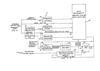
FIGURE 1 shows a block diagram view o~ the first embodiment
o~ the invented micro-machine/interface o~ the present invention;
PIGURE 2 shows a timing diagram illustrating certai~ signals
which are transmitted or asserted during a typical operation o~
the micro-machine/inter~ace o~ FIGURE l;
FIGURE 3 shows an e~ploded block dlagram view of the
sy~chronization/synchronization assist component o~ FIGURE l;
~ IGI]RE 4 shows an exploded block diagram vie~ o~ a
synchronization/synchronization assis~ o~ a second embodiment of
the invented micro-machine/interface;
FIGURE 5 sho~s a block diagram vie~ oi a third embodiment o~
the invented micro-machine/interface;
FIGURE 6 shows an e~ploded block dlagram view of the
synchroni~ation/synchronization assist o~ the micro-machine/
inter~ace o~ FIGURE 5.
BB2/smg/SUN/~21
~29(~58
1 DETAILED DES,RIPTION OF THE PREF~RRED EMBODI~ENTS
In the follo~ing descript1On ~or purposes o~ e~planation,
bits, logic blocks, timing relationship, etc. are set ~orth in
order to provide a thorough understanding o-~ the present
invention. However, it will be apparent to one skilled in the
art that the present invention may be practiced without the~e
speci~ic details. In other instances, ~ell k~own circults and
device~ are shown in block diagram ~orm in order not to obscure
the present invention in unnecessary detail.
In Figure 1 there is shown a general block diagram oY the
first ~mbodiment oi the invented micro~machine/inter~ace denoted
g~nerally by re~erence numeral 9.
I~ Figure a there is shown a tlming diagram illustrating
certain signals ~hich are transmitted or as~e~ted during the
operat.ion o~ the micro-machine/inter~ace o~ Figure 1. Operation
o~ the micro machine interiace o~ Figure 1 will be described in
con~ux~ction ~ith reference to Figure 2, however, Figure 2
repre~;e~ts only an illustrative timing dlagram o~ the execution
o~ a particular instruction under the condition in which the
micro-machine/lnter~ace 9 is not e~ecuting a previous instruction
~hen the i~coming instruction arrives. Operation o~ the mlcro-
machine/inter~ace 9 ~ill later be described in a situation
wherein a previous instruction ls being e~ecute~ when the
incoming instruction arrives.
In the example instruction employed to illustrate the
operation o~ the Pirst embodiment o~ the micro-machine/inter~ace
~ of Figure 1, the incoming instruction is asserted by the CPU 10
sometime during clock cycle ~-B o~ Figure 2. The particular
incoming instruction used as an e~ample herein requests the
6 BB2¦smg¦SUN/921
;8
1 addition of the operand contained in ~he incoming instruction and
the contents of reglster 1 of the register files 40A of data path
elements 40. The incoming instruction in the example instruction
herein described contains an operand, an op code, and a user
5 register address. It will be appreciated however that the
micro-machine/interface 9 is capable o~ performing many other
types of instructions (e.g. vector additlon, subtraction, etc.)
and is not restricted to e~ecuting only the exemplary addition
lnstruction, the particular instruction described herein being
10 merel~ for purposes of illustration and clarity with respect to
operation of the micro-machine/interface 9.
A command register 55 enters an "idle state" upon the
completion of every instruction. For purposes of the
Specl~ication herei~, "idle state" i~ defined as the period of
15 time cluring which the command register 55 is not e~ecuting the
routiDe o~ an incoming instruction (i.e. the period of time
durin~ which the command register 55 is frozen and is not
clocking through the commands of the routine associated with an
incoming instruction). Since, in the example operation first
20 described herein, a previous instruction was completed pric~ to
clocX A o~ Figure 2, the command register 55 is in the idle state
when 'che incoming instruction arrives (The idle stzte of command
register 55 will be discussed in greater detail below.)
Further, since the clock of the micro-machine/interface g,
25 and the clock of t~e CPU 10 are asynchronous from one another,
the phase relationship between the clock of the CPU 10 and the
clock o~ the micro-machine/interface 9 is not known. Therefore~
the incoming instruction is not synchroni~ed to the clock of the
micro-machine/interface 9 until one to two clock cycles after
30 arriva~ oP an in&truction control signal (shown on Figure 23 that
7 BB2/smglSUN/g21
8~8
1 indicates the arrival of an incoming instruction. One clock
cycle a~ter synchroni~ation o~ the lncomin~ instruction, the
command register 55 leaves its idle state and begins e~ecuting
the incoming instruction (i.e. begins clocki~g through the
5 comma~ds o~ the routine o~ the incoming ins~ruction).
Accordinglyr since, in the example operation described herein,
the incoming instruction arrives during clock cycle A-B, the
command register 55 is in its idle state until clock D o~ ~igure
2.
~s stated, in prior art asynchronous m1cro-machine s
synchronization o~ the incoming instruction~ as well as trans~er
o~ control to the routine o~ the incoming instruction must occur
be~ore any actions ~or the instruction take place. In direct
contrast, the invented micro-machine/interiace 9 initiates
15 actions ~or the incoming instruction be~ore e~ecution of the
i~structlon beglns (l.e. be~ore the command register 55 beglns
cloc~ing through the commands o~ the routine of the incoming
instruction) and during trans~er o~ co~trol to the routine o~ the
incomin~ instruction.
The above has been made possible through the novel
imple~entation o~ the fact that many actions are common to the
vast majority o~ instructions (i.e. the channeling o~ an operand
to an arithmetic UDit, the channe1ing o~ a register ~lle address
to a register ~ile, etc.)
~ will later be explained in greater detail, this is partly
achieved by varlous control signals which are loaded lnto command
register 55 upon th~ completion o~ every instruction and which
collectlvely compriæe a single command which is re~erred to
herein as the "idle state co~mand". As will als~ later be
30 explained in more detail, the actions which take place prior to
8 BB2/s~g/SUN/921
~s30~5~
1 e~ecution o~ the incoming instruction and during transier of
control to the routine o~ the incoming instruction is also
achieved by a synchroni~ation/synchronization assist circuit 60
which determines when these actions take place~ The above
m~ntioned control slgnals o~ which the idle state command is
comprised are stored in a memory location, of a microstore 50,
that is associated ~ith the operation of the micro-machi~e/inter-
~ace 9 when the command register 55 is in the ldle stateO Upon
tb~ completion of an instruction, all routines trans~er control
10 to that; memory location and the idle state command stored
therein. Since the command register 55 asserts the control
signals oP the idle state command while the same is in the idle
state, it causes the per~ormance of actions common to mo~t
incoming instructions prior to e~ecutlon o~ the commands
15 specifLed by the routine o~ the incoming instruction and duri~g
transfer o~ control to that routine, thereby ~reatly decreasing
latenc~. These control signals are divided into five major
groups and will be discussed below with reference to Figures 1
and 3. It is important to note that some of the control
20 signals of the idle state command are also asserted by command
register 55 when it is not in its idle state is (i.e. when it is
e~ecuting the incoming instruction), the important dif~erence
being that the signals which are loaded in the command register
55 after the command register 55 leaves the idle state are a part
25 of the routine that is associated with the incoming instruction,
whereas the control signals asserted by the command reglster when
it is in the idle state are ~ot.
A ~irst group o~ the control sig~als which the command
register 55 asserts when in the idle state are termed herein as
30 'ridle signals", which the command register 55 transmits to a
9 BB2Jsmg/SUN/9~l
s~
1 synchronization/synchronization assist circuit 60. These idle
signals inform the synchronization/synchronization assist circuit
60 that the command register is in its idle state and are also
channeled through synchronization/synchronization assist circuit
5 60 to instruction latches 20 and parameter latches 30 ~as
indicated in Figure 1) and, upon assertion thereat, open
instruction and parameter latches 20 and 30 such that they are in
their open ~iOe. flow through) mode when the command register 55
is in the idle state (in our e~ample operation until clock D ln
10 Figure 2). When the command reg~ste~ 55 leaves its idle state,
(in the e~ample operatlon described herein at clock D) the idle
slgnal~i are deasserted. Deassertion by the command register 55
o~ the idle signals closes latches 20 and 30 such that the same
capture the information that has been flowing therethrough, and
15 thu~, the lnformation transmitted continues to be transmitted by
their reSpective outputs until latches 20 and 30 are opened by
reassertion o~ the idle signals upon completion of the e~ecution
o~ the incoming instruction.
A second group of the iive groups of controls signals that
20 the command register 5~ transmits when in the idle state are
sign~ls ~hich multiplex incoming instruction information that is
transnlitted to data path elements 40 and are termed herein, as
"data path multiplexing control signals". A predetermined set o~
these slgnals are asserted when the command re~ister 56 is ln the
25 idle state.
Si~ce, i~ the e~ample operation described hereln,
instruction latches 20 are in their open ~flow-through) mode upon
the arrival of the incoming instruction (i.e. sometime between
clock cycles A to B, as shown in Figure 2 and hereina~ter
30 "arrival'l), the operand of the ~ncoming instruction ~lows through
BB2/smg/9UN~921
~o~
l instruction latch 20 to data path elements 40 and the data path
multiplexing signals issued by command register 55 ~hile in the
idle state channel the operand of the lncoming instructlon to
arithmetic units 40B of data path elements 40, also upon arrival
5 and before clock D.
~ lso upon arrival, the incomlng lnstruction is asserted at
the input of the instruction translatlon 15. Instruction
tra~slation 15~ in the pre~erred embodiment, comprises a mapping
RAM 15A and an i~struction decode 15B~
The instruction decode 15B o~ instruction translation 15
recei~es the user register address specified in the incoming
instruction and t~anslates the user register address into the
the register ~ile add~ass of the register ~iles 40A (in our
exemplary lnstruction register 1~. The register file address is
15 transmitted along parameter registers by-pass 26 to data path
elemen.ts 40 and to parameter registers 35 by i~struction decode
15B of ins~ruction translation 15, in the e~ample operation
described herein, sometime after arrival and before clock D. The
register file address transmitted along parameter registers by-
20 pass 26 is channeled by corresponding data multiplexing control~ignals which are transmitted by command register 55 to data path
elements 40 when the command register 55 is in t~e idle state, to
the acldress inputs of the register files 40A o~ data path
elements 40, sometime between arrival and clock D. The register
2~ file address channeled to the address inputs of the register
~iles 40A begins the reading of the register addressed and thus
initiates the outputting of the contents o~ that register (in our
e~ample, re~ister 1 o~ the register ~iles 40A).
With respect to parameter registers 35, loading o~
30 parameter registers 35 is controlled by load enable signals
11 BB2/smg/~U~921
~.~<~0~
1 asserted by synchronlzation/synchronization assis* circuit 60 to
parameter registers 35 and these signals are not asserted until
a~ter the command re~i~ter 55 leaves its idle state.
Accordingly, in the e~ample instruction herein described, the
5 above mentioned register ~ile address i6 not clocked into
parameter registers 35, and as such, ls not valid at the output
o~ parameter registers 35, until a~ter clock D~
Since in the e~ample operation herein described the command
re~ister 55 deasserts ~he idle signals at clock D, and thus
10 latches 20 and 30 are thereby closed at clock D, the operand
which, prior to clock D, was ~lowing through instruction latches
20 is thereby captured by instruction latches 20 and remai~s
valid at the output of the same until the previously mentioned
idle sLgnals are reasserted upon the completion o~ the routine of
15 the incoming instruction. It will be appreciated that the
operand which is captured by instruction latches 20 at clock D
and which is valid at the output o~ instructlon latches 20 may be
used again throughout the routine when an error occurs.
The address ~ield o~ the incoming instruction ~which in our
20 speci~ic e~emplary incoming instr~ction is comprised o~ the
instruction op code and the user register address) is channeled
to th~ address inputs o~ mapping RAM 15A, and causes the
outputting, by mapping RA~ 15A, o~ instruction control bits that
designate what type o~ operation (i.e. addition, multiplication,
25 etc.) and what type o~ operand (i.e. single precision, double
precislon etc.) are associated with the incoming instruction.
These instructio~ control bits are outputted by mapping RAM 15A
~ometime a~ter arrival and be~ore clock ~ and are transmitted
through parameter latches 30 to data path elements 40.
The instruction control bits that designate what type o~
12 BB2/smg/SU~/921
1 operand is contained in the incoming instruction are channeled to
the arithmetic unlts 40B by corresponding data multiplexlng
control signals which are tranmsitted by command register SS to
data path elements 40 while the command register 55 iæ ln its
5 idle state. ~s will later be discussed, tile instruction
control bits that designate what type o~ operation is requested
by the incoming instruction are not utilized within data path
elements 40 until aft~r the command register 55 leaves its i~le
state.
In the e~ample operation herein described, as stated,
parameter latches 30 are closed at clock D so that the previously
mentioned control bits which designate what type o~ operation is
requested by the incoming instruction are thereby captured by the
parameter latches 30 and are continuously asserted and at the
-15 output of the same until the command register 55 reasserts the
idle ~ignals.
I'he control bits which designate what type of operation is
requested by the incoming instruction are channeled after clvck D
by the! commands outputted by the command register 55 which are
20 a part; of th~ routine of the incomin~ instruction to
arithmetic units 40B, thereby instructing the arithmetic unit 40B
as to what type of operation it must perform. It is important to
note that many instructions (for example, addition, subtraction)
di~fer from one another only in the value o~ the control bits
25 associated with each instruction that designate what type o~
operation is r~quested.
In prior art devices these control bits are stored in a
microstore with a di~ferent set of commands for each routine. In
the present invention, since these control bits are derived from
30the incoming instruction by the instruction decode 15B and are
13 BB2Jsmg/SUNJ921
0~8
l not stored in microstore memory 50, the same routines may be used
-~or many different instructions, thereby minimizing the amount o-;
microstore space req~ired ~or storing commands.
In vie~ of the above discussion, it will be app~eciated that
5 the aspect o~ the present invention wherein control bits that
desi~nate what type of operation is requested by the incomin~
instruction and what type o~ operand is contained therein may
also be e~icaciously used ~ith micro-machines which are syn-
chronous ~lth the master CPU (i.e. where the clocks o~ the micro-
lO machine and the CPU are in phase with one another~ since the
abo~e clescrlbed result e~ect, (i.e. minimizing that amount o~
micros~ore space required ~or storing commands) can be achieved
in both synchronous and asynchronous micro-machines when this
aspect o~ the present invention is employed.
The address ~leld o~ the incoming instruction which, as
stated" ls channeled to the address lines oi the mapping RAM 15A,
also speci~ies a mcmory location within mapping RAM 15A that
contains the routine starting address that is associated with the
incoming instruction.
Sometime between arrival and cloc~ D o~ Figure 2, the
mapping RAM 15A transmits the instruction routine starting
address to the input 41 of ne~t address generation 45. Since, as
previously discussed, in the example operation herein described,
command register 55 ls in its idle state until clock D,
25 predetermined values o~ a third group, o~ the previously
discussed ~ive groups o~ control signals, termed herein as "next
address control slgnals" are asserted at the input 43 o~ next
address generation 45 sometime prior to clock D. These ne~t
address control slgnals instruct the ne~t address generatio~ 4S
30 to cbannel the instruction routlne startlng address, ~hich was
14 BB2/smg/SUN~921
1 transmitted to input 41 of ne~t address generation 45, through
ne~t address generation 45 to the address lnputs o~ the
microstore 50. After clock D, next address control signals,
~hich are specified by the routine of the incoming instruction,
5 are asserted at input 43 of ne~t address generation 45 and
instruct the ne~t address generation 45 to ignore the routine
starting address of the incoming instruction and also instruct
the ne~t address generation 45 how to generate the remainin~
microstore addresses associated w~th ths routine of the incomlng
10 instruction (i.e. sequential addresslng, ~ump, call, return
~tc.~. Th~ next address control signals asserted by command
register 55 which are specified by the routine of the incoming
instructio~ determine corresponding memory locations ~ithin
mlcrostole 50 wherein are stored the remaining commands of the
15 routine of the incoming instruction.
The instruction routine starting address of the lncomin~
instruction is asserted at the address inputs of mlcrostore 50
so~etime after arrival a~d be~ore clock D and specifies a memory
location within microstore 50 which contains the first command o~
20 the routine of the incoming instruction. Microstore 50, in turn
asserts the ~irst command at the input 51 of command register 55.
As prevlously discussed, in the specific example described
herein, command register 55 ls in lts idle state and is ~rozen
until clock D. Accordingly, the ~irst command of the i~coming
2S instruction, which in our e~ample is asserted at the input of
command register 55 sometime between arrival and clock D, is not
clocked through command register 55 until after the command
register 55 leaves its idle state at clock D. The clocking of
command register 55 ~ill later be discussed with reference to
30 Figure 3.
BB2/smgtSUN/921
~ 3oa~
1 Operat~on o-~ synchronization/synchroni~ation assist circuit
60 o~ Figure 1 will no~ be discussed in detail with re~erence to
Figure 3 in addition to Figures 1 and 2. In Figure 3 there is
shown an e~ploded block dlagram o~ the components of
synchronizatlon/synchronization assist circui~ 60. X~struction
control signals are transmitted by CPU 10 to a~ instruction
decode circuit 62 o~ synchronization/s~nchro~ization assist
circuit 60 bet~een, in the e~ample operation herein described9
clo~k cycles A-B o~ Figure 2. These instruction control signals
indicate the arrival o~ the incoming instruction which has been
previously described with re~ere~ce to Figure 1.
The instruction decode circuit 62 determines whether or
not a ~alid access is being requested by the CPU 10 and, i~ a
valid access is being requested, asserts the input o~ flip ~lop
ff4, l~lip ~lop 64 is clocked by the clock o~ the micro-ma-
chine/inter~ace 9, and, accordi~gly, at clock B a synch 1 signal
is asserted at output Q o~ ~lip ilop 64 and lnput D o~ flip ~lvp
6~. The synch 1 slgnal is shown in Figure 2. ~lip ~lop 66 ls
also c.oupled to the Glock o~ the micro-machine and, accordi~gly,
at clock cycle C, the sy~ch a signal is asserted at the output Q
o~ ~lip ilop 62. The synch 2 signal is shown on Figure 21 The
synch 2 signal outputted by ~lip flop 6~ is, in turn~ asserted at
the input 61 o~ command register clock control circuit 69, the
input 65 o~ decode oi shared control signals circuit 72, input 82
2s o~ decode ack~owledge signal circuit 80 and lnput 76 of register
an~ latch control 88. Also, as shown in Fi~ure 3, input 63 of
reglster clock control circuit 69, i~puts 67 and 73 o~ decode o~
~hared control signals circuit 72, ~nput 81 o~ decode o~
acknowledge signal circuit 80 and, i~puts 77 a~ 78 o~ register
and latch control circuit 88 are coupled to the output 53
o~ the command register 55 o~ Figure 1, in order to
16 BB2/smg/SUNl921
l receive vario~s control signals there~rom as discussed below.
The decode of shared control signals clrcuit 72 is coupled to
data path elements 40 and asserts shared control signals which
initiate actions ~or the incoming instruction, wlthin data path
5 elements ~0~
A ~ourth group of the control signals ~hich the command
register 55 asserts when in the ldle state are termed herei~ as
"signa].s whi.ch correspond to shared control signals" and are
discus~ed belo~. (Note: these signals are also transmitted as a
lO part oi the routine o~ all instructions). Note also; as
previously discussed, all o~ the control signals ~hich are
transmitted by the command register 55 when it is in lts idle
s~ate ~re taken from a memory location o~ microstore 50 wherein
is stored the idle state command and all of the control signals
15 whicb the command register 55 asserts when it is not in its idle
~tate are taken from memory locations o~ the microstore 50
wherein are stored the commands which comprise the routine.
A particular shared control signal is asserted by decode o~
ahared control signals 72 whenever: (i) a control signal
20 corresponding to a particular desired shared control signal ls
asserted at input 67 by the command register 55 and the idle
signals (which are also transmitted by the command register 55)
ar~ deasserted at input 73 or; (ii) a signal corresponding to a
particular desired shared control signal is asserted at input 67,
25 idle signals are asserted to input 73 and the synch signal 2 is
assert~d to input 65. As stated, when the command register 55
is in the idle state it asserts predetermined signals ~hich
correspond to shared control signals. Thus, in the e~emplary
instruction previously described with re~erence to ~igure 1,
30 some~ime be~ore clock D a ~irst predetermined shared control
17 BB2/smg/SUN/921
~2~3~)~35~3
l signal (shown on Figure 2) is asserted by decode o~ shared
control signals circuit 72, to the arithmetic unit 40B oi data
path elements 40. This ~irst predetermined shared control signal
triggers the loading of the operand o~ the incomin~ instr-i¢~ion
S lnto the arithmetic unit 40B at clock D.
The command register clock control circuit 69 of Figure 3 is
coupled to the clock enable input 52 o~ the command register 55-
o~ Figure 1 and ls also coupled to the clock o~ the micro~
machine/inter~ace g. One clock cycle a~ter the point ln time at
lO which both the synch 2 signal and the idle signals are asserted,
respect~vely, at inputs 61 and ~3, ~i.e. in the example operation
herein described at clock D) the command register clock control
circult ~9 enables the clock oi' the command register 55, such
that the same ;eaves its idle state and clocks through the ~irst
. ~5 command speci~ied by the routine starting address of the incoming
instruction which had previously been asserted at input 51 o~ the
comm~d reglster 55, in the manner described with re-Eerence to
Figur~
Therea~ter, during the remainder oi the routlne of the
20 incomj.ng instruction the clock o~ command register 55
continues to be enabled by the register clock control circuit 69
until the command register 55 indicates, to the register cloc~
control circuit ~g, the completion o~ the incoming instruction by
reasserting the previously dlscussed idle signals at the input ~3
25 thereo-~. After being enabled by command register clock Gontrol
circuit 69, as described with re~erence to ~'igure 1, the command
register 55 continuously asserts ne~t address control signals,
which are speciiied by the routine, at input 43 oi the ne~t
address generatioD circult 45 o~ Figure 1, such that the ne~t
30 address generation circuit 45 continuously sequences through
18 BB2~smg/SUNI921
~.X9()~i8
l memory locations o~ mlcrostore 50 such that microstore ~0
continuously outputs the remaining commands o~ the routine to the
input 51 o~ command register 55~
The decode acknowledge circuit 80 issues an acknowledge
signal to the CPU 10 at the ne~t rising transition of a clock
after comman~ register idle signals are asserted at input 81
thereo~ and the synch 2 signal is asserted at lnput 82 o~ the
same. Mote: because the incoming instruction is captured in the
instructlon latches 25~ parameter latches 30 and parameter
r~gisters 35 o~ Figure 1, when the command register 55 leaves the
idle state, as previously discussed with re~erence to Figure ~
transmission o~ the incoming instruction by the CPU is no longer
required a~ter clock D.
~'ith re~erence to the register and latch control circuit 88
o~ Fii;ure 3, output 94 thereo~ is coupled to the enable inputs o~
inst~,ftion latches 20, output 96 is coupled to the ena~le inputs
o~ the parameter latches 30 and output 98 is coupled to the
load/count/hold control inputs of parameter registers 35.
The register and latch control circuit 88 channels, via
~ outputs 9~ and 96, the idle signals which open, respectively,
instruction latches 20 and parameter latches 30 whenever command
register idle signals are asserted at input 77. As stated with
re~erence to Figure 1, when these idle signals are deasserted by
command register 35 at input 77, the instruction latches 20 and
parameter latches 30 become closed.
A iifth group oi the control signals which the command
register S5 transmits when in the idle state are termed herein as
"parameter registers con~rol signals". The parameter registers
control signals are transmitted by comman~ reglster 55 to the
~o register and latch eontrol circuit 88 at input 78. These
19 BB2/smg/SUN/921
l parameter registers control signals play a role ln the outputting
of load/hold/count signals output-ted by register latch control
circuit 88 in the ~ollowing way: 1.) If the ~dle signals are
asserted at input 77 and the synch 2 signal is asserted, at lnput
7~ the registers will be loaded at the next transition o~ the
clock of the micro-machine/inter~ace. 2.) During instruction
exeuction (i.e. idle signals are not asserted at input 77) the
synch 2 signal is ig~ored and the parameter registers control
slgnals asserted by command regsiter 55 at lnput 7B are routed
directly to the parameter registers 35.
As state~, ~or purposes o~ illustration, operation o~ tbe
mic~o-machine/interface 9 o~ Figure 1 in its execution o~ an
e~emplary instruction (the addition o~ the operand to the
contents of register 1) has been described. ~owever, as
mentioned, the micro-machlne/inter~ace 9 may e~ecute a ~ull range
o~ more complicated instructions such as, ~or example, vector
addition, ve~tor s~;btraction, etc. In a sltuation wherein a
vector addition is re~ues~ed by the incoming instruction, the
countLng o~ the parameter registers 35 will be enabled during
several clock cycles over the course o~ the execution of thP
instruction in the manner previously discussed with re~ersnce to
Figure 3, thereby incrementing or decrementing the register
~ile address stored in the parameter registers 35. It will also
be appreciated that additlonal registers may be employed ~ith the
invented mi~ro-machine/inter~ace 9, in a similar manner as are
parameter registers 35, to per~orm register operations upon
direct untranslated portions o~ an incomlng instruction.
In the e~ample operation herein describedl aYter the ~ommand
register 55 leaves its idle state it aæserts data multiplexing
signals to data path elements 40 which channel the contents o~
BB2/smg/SUN~921
~L2'30~358
1 the information read ~rom register 1 of register ~iles 40A to the
arithmetic unit 40B o~ Figure 1. Also, the command register 55
transmits a signal ~hich corresponds to a second shared control
signal to synchro~ization/sy~chroni~ation assist circuit 60
which, i~ turn, asserts a second shared control slgnal to data
path elements 40 that initiates the loading o~ the contents of
Register 1 o~ the register ~iles 40B into the arl$hmetic units
40A and which also i~titiates the adding therein o~ the opera~d
(which had been previously loaded into the arithmetic unit 40B by
the first shared control signal) and the information that h~s
been read ~rom register 1.
The add operati(~n initiated by the assertion of the second
shared. control signal continues until sometlme bet~een clock
cycles E to ~ of Figure 2. Accordingly, sometime a~ter clock E,
the addition is completed a~d command register 55 transmlts
further commands speciiied by the routine which channel the
outpu1; of the arithmetic unit to the register files 40A, verifies
that no errors were made during the addition of the operand and
the contents o~ register 1, channels the register file address
(which, as discussed is valid between clock cycles D to n at the
output o~ parameter registers 35) to the address inpu*s o~ the
register ~iles 4QB and writes the results of the addition
operation into register 1 thereof.
The above-discussed e~ample operation of the micro-machine/
interface 9 occured in a situation wherein an incomiDg
instruction arrived sometime between clock cycles A-B and a
previous instruction was not being executed by the micro
machinelinterface 9 during clock cycle A-Bs such that, command
register 55 was in its idle state when the incoming instruction
arrived.
21 BB2/smglSUN/921
~2~
l In a situation wherein the micro-machine/interface 9 is
completing a previous instruction upon arrival o~ a new incoming
instruction and, for example, the command register 55 comple$es
the previous instruction at clock n, the command register 55 will
5 enter the idle state at clock n and begin execution o~ the new
instruction one clock cycle later. ~ote, that because in this
situtation the command register 55 is in its idle state at clock
n9 *he previously described actions, which are triggered by the
~ive groups o~ control s~gnals that the command register 55
10 transmits ~hen i~ idle, take place~ Also, because the
synchr~nization/synchronization assist circuit 60 recogni2es that
the new incoming instruction has arrived, the command reV~ster is
not re,~uired to e~ecute commands which have been ~etched ~rom
~icrostore space iD order to determine i~ a new instruction has
15 arrived (as previously discussed with re~erence to Figures 1~ 2
and 3), as are all command registers o~ prior ært asynchronous
micro--machines. As such, it ~ill be appreciated that even ln
situations wherein a previous instruction is being e~ecuted when
a new incoming lnstruction arrives, latency is greatly reduced.
~lso, as indicated with re~erence to Figure 1, whlle a
previous instruction is e~ecuting the routine starti~g
address o~ the new incoming instructlon outputted by mapping RA~
15A of i~struction translation 15 to ne~t address generation ~5
(o~ Figure 1) will not be channeled to microstore 50 untll the
~S command register 55 enters its idle state a~d asserts appropriate
ne~t a~dress control signals at input 43 o~ ne~t address
generation 45 to sequence the routine starting address thr~ugh
next address generation 45 to microstore 50 as prevlously
described.
22 BB2/smg/SUNl92I
gc~3r~
l The micro-machinelinter~ace 9 o~ Figures 1 and 3 is designed
to e~ecute single access instructions (i.e. when the instruction
address ~ield is not larger than the address bus o~ the master
CP~ and the data fleld of the incoming instruction is not larger
5 than the data bus of the master CP~). It will be appreciated
that instructions in which the instruction address ~ield is
lar~er than the address bus o~ the master CPU or in which the
data ~ield is larger than the data bus o~ the master CPU must be
transm:Ltted to the micro-machine/interface 9 in two accesses.
In Figure 4 there is shown an e~ploded block diagram view oi
a ~ynchronization/synchronization assist circuit 60A, which, when
used in place of synchronization/synchronizatlon assist circuit
60 of Figures 1 and 3, provides a second emhodiment oi the micro-
machine/interface 9 for egecuting two access instructions.
It will be observed that the synchronization/synchronization
assist circuit 60A for two access instructions o~ Figure ~
di~ers irom the synchronization/synchronization assist circuit
60 o~l~igure 3 in that the ~ormer has two additional flip flops
95 and 97. As with ~lip flops 64 and 66, flip fIops 95 and 97
20 are coupled to the output o~ instruction decode circuit 62,
command register clock control circuit 69 at input 89 thereo~,
decode o~ shared control signals circuit 72, decode acknowledge
signa]. circuit 80 and register and latch control circuit 88.
In a two access instruction, first and second instruction
25 control signals are asserted respec-tively, by the CPU 10 at
instruction decode circuit 62. A first instruction control
~ignal is asserted when the ~irst half of a two acces~
instruction is transmitted to the micro-machinelinter~ace 9 and a
second instruction control signal is transmitted when the second
30 half of a two access instruction is transmitted by CPU 10~
23 BB2/sm~/SUN/921
1 Assuming that command register 55 is in a ~irst idle state
upon the assertion of the first instruction control signal
indicating the arrival of the ~lrst access of the two access
instruction, the actions previously described with reference to
5 Figures 1, 2 and 3 take place e~cepting that upon completion o~
the portion of the routlne associated with the ~irst access of a
two accesæ instruction the command re~ister 55 enters into a
second idle state a~d transmit a command that is associated with
that second idle state. Synchronization/synchronization assist
10 60A will then disable the clock of the command register 55 until
the sec~nd access of the two access lnstruction ls synchronized9
as discussed below. Unlike the iirst idle state, in a t~o access
instruction, the command outputted by the command register 55
when in its second idle state is a part o~ the routine of the two
15 access instruction. The second idle state and its associated
idle state ~ill also later be discussed~
Aiter the first access of the two access instruction has
~een a.ccepted and the 5PU has received a first acknow ledge signal
outputted by decode acknowledge signal circuit 80 in the manner
20 previously described with reference to Figure 3, the CPU will
transmit the second access and its associated second ~nstruction
cont.rol signal.
The second instruction control signal will be asserted at
instructio~ decode clrcuit 62 and the same will, in turn, assert
25 the input D o~ ~lip ilop 95 such that, one clock cycle later, a
synch lA si nal is asserted at output Q o~ flip flop 95 and input
D o~ ~lip ~lop g7. One clock cycle after assertion o~ the synch
lA signal, a synch 2A s~gnal is asserted at the output Q of ~lip
ilop 97 and thus at the input 89 of command register clock
control circuit 69, the input 92 o~ decode o~ shared control
24 BB2/smg/~UN/921
J xsoa~
l signals c~rcuit 72, the input 90 o~ decode acknowledge signals
circuit 80 and the input 93 of latch and enable control circuit
88. The synch 2A signal plays the same role in e~ecution of the
second half of the two access instruction as did the synch 2
signal in e~ecution o-E the first half of the lncoming two access
instruction. Accordingly 9 one clock cycle a~ter the assertion
of synch 2A and the assertion o~ the idle signals, the clock
command register 55 is enabled, the same leaves the second idle
state and a second acknowledge signal is se~t to CPU lO.
Note, in the second embodiment, since the routine starting
address is not asserted during the second access, it is not
emplo~ed in the second access.
In the two access instruction ambodiment of Figure 4, there
are t~o groups o~ idle signals transmitted by command reg~ster 55
durin~, respectively, the irst and second idle states.
Asser1;ion and deassertion of the ~irst group oi idle signals
triggers the outputting by latch and register control circuit 88
of instruction latches enable signals and parameter latches enable
signaLs at, respectively, outputs 94 and 96 which> respectively,
open and close a first plurality of latches of instruction
latches 20 and parameter latches 25 in the manner previously
discussed with reference to Figures l and 3. The first
plurality of latches o~ instruction and parameter latches 20 and
25 capture portions of the first access ~f the two access
incoming instruction.
A second plurality of latches o~ instruction and parameter
latches 20 and 25 transmit and capture portions of the second
access o~ ~he two access incoming instruction. Instruction latch
enable signals and parameter latches enable signals are asserted by
re~lster and latch control circuit 88 to the second plurality of
~5 BB2/smg/SUN/92l
~908~
1 latches such that the second plurality o~ latches are open ~rom
the assertion o~ the ~irst group of idle signals and a~ter
deasser$ion o~ the same until the deassertion o~ the second group
o~ idle signals.
Similarly, with reierence to the parameter registers 35 o~
Figure 4, a first plurality of parameter registers o~ param~ter
registers 35 capture and transmit portions of the first access ~i~
the two access incoming instruction. The ~irst plurality o~
parameter registers are triggered to load the portions of the
~irst access of t~e two access lnstruction, when the command
register leaves the iirst idle state, by load signals outpu~ted
~y register and latch control c1rcuit 88 of Figure 3 at output 98
thereof. A second plurality of registers o~ parameter registers
35 capture and transmit portions oP the second access o~ the
lncominK two access i~structlon when the command register leaves
the second idle state thereby trlggering register and latch
control circuit 88 to output appropriate load signals to *he
second plurallty o~ registers.
After completion of the ilrst access o~ the two access
2n illstrv.ction, when the command register 55 enters into the second
idle state, control signals are asserted by the same which, in
conjunction with synchronlzation/synchronization asslst circuit
60A perform actions associated ~ith the second access prlor to
the execution oi the same. These second idle state ~ctions are
ini~iated in the same manner as are the idle ~tate actions t-~ch
have been previouslg discussed with reierence to Figures 1 - 3.
Further9 in the second embodiment of the micro-machine/in-
ter~ace 9, the command register 55 does not have to e~ecute any
instructlons to determine 1~ the second access ~as arrived and so
that execution of the ilrst hali oi the two access instruction
2a BB2/smg/SUNI971
~9~
1 will begin prior to the arrival of the second access o~ the t~o
access 1nstruction.
In Figure 5 there is shown a third embodi~ent o~ the
invented micro-machinelinterface 9 having an incoming instruction
pipeline so that the micro-machine/interface 9 ~ay hold and begin
to translate and synchronize an incoming instruction ~hile a
previous instruction is being e~ecuted. It ~ill be observed that
the third embodiment o~ the "pip~line" micro-machi~e/inter~ace 9
oi Figure 5 dif~ers from the ~ir~t embodiment o~ the micro-
machinejinter~ace o~ Figure 1 in that the former employs ne~tinstruction latches 8 and a different synchronization/~ynchron-
ization assist circuit 60B.
For ~urposes o~ illustration of the opera.tion o~ the third
embodi.ment o~ the micro-machine/inter~ace 9 of Figure 5,
.oper~tion of the micro-machine/interface 9 will be described in a
situat:ion wherein the micro-machine/interiace 9 is not e~ecuting
a pr~lous instruction when an incoming instruction arrives.
Under such a condition, next instruction latches 8, instruction
latches 20 and parameter latches 30 will be in their open ~low
through mode~ Accordingly, upon transmission of an incoming
instruction by GPU 10, next instruction latches 8 will channel
throul3h the incoming inætruction to the remainder o~ the micro-
machine/i~terface 9 and the same will begin to perform the
actions for the incoming instruction in the manner previously
described ~ith re~erence to Figure 1. However, shortly aiter
arrival oi the incoming instruction, synchronization/synchron-
iz,ation assist circuit 60B deasserts the enables o~ ne~t
instruction latches 8 thereby closing next instruction latches 8
such that the incoming instruction is captured in ne~t
instruction latches 8 shortly a~ter arrival of the incoming
2q BB2/sm~/SUN1921
~;~9(~ i8
1 instruction. Synchronization/synchronization assist circuit 60B
then sends an acknowledge slgnal to the CPU 10 such that the
incoming instruction is no longer transmltted by the CPU 10 and
the same is then free to transmit another incoming instruction.
Thereafter, the actions previously described with re~erence to
Figure 1 $ake place, and instruction latches 20 and para~eter
latches 30 are closed ae previously described. A~ter the
closing o~ instruction and parameter latches 20 and 30, the
synchroni~ation/synchronization assist circuit 60~ reasserts the
enables o~ the ~ext instruction latch~s 8 thereby opening the
next instruction latches 8 such that the same may receive and~ in
turn, capture a new second incoming instruction.
Accordingly, shortly a~ter arrival o~ a second incoming
inætruction, ne~t instruction latches 8 are again closed such
that the second incoming instruction is captured in next
instrurtion latches 8 and the CPU 10 receives another acknowledge
signal transmitted by synchronization/synchronization assist
circui~ 60B. Since the next instruction latches 8 have bee~
closed to capture the incoming instruction, the same is valid at
the output oi the next instruction latches 8 and available ior
use by the micro-machine/inter~ace 9 as previoiusly describe~
with reference to Figure 1.
In Figure 6 there is shown an exploded bloc~ diagram of
synchronization/synchronization assist circuit 60B ~or the
pipeline micro-machlne/inter~ace o~ Figure 5.
As illustrated in Figure 6, instruction decGde circuit 62
receives the acknowledge signal outputted by decode ackno~ledge
signal circuit 80. When an incoming instruction is lndicated by
an lnstruction control signal at the input of instruction decode
circuit 62, instruction decode circuit 62 deasserts the enables
2~ BB2/smg/SUN~9~l
3~3~3~
1 of ne~ instruction latches 8 thereby closing the same and
capturing the lncoming lnstruction flowing through the next
instruction latches 8. A~ter the ne~t instruc~ion latches are
closed, the decode ackno~ledge signal 82 sends an acknowledge
signal to the CPU 10. ~Note, because the instruction is
captured in ne~t instruction latches 8 (as opposed to registers~,
latency is not increa~ed by the addition of the pipeline
comprised o~ the next instruction latches 8 o~ Figure 5.] A~ter
rec~ipt of the acknowledge signal outputted by decode ac~nowle~ge
sign~l circuit 80, instruction decode circuit 62 then asserts the
enable~ of ne~t instruction latches 8 thereby opening next
instruc*ion latches 8 and releasing the instruction ~tored
thereill ior e~ecution of the instruction in the manner previously
descril~ed with re~erence to Figure 1~ At this point in time, the
next i~lstruction latches 8 are ready for receipt and capture oi
second incoming instruction in the manner previously described
with re~erence to Figure 5.
It will be appreciated by those skilled in the art that the
embodi.ments o-~ Figures 4, 5 and 6 may be combined as a single
micro-machine/interEace in order to perform all of the functions
previously described with re~erence to the two embodiments.
It will be appreciated that the present invention may
also be employed in a situation wherein the clock which runs the
micro-machine is in phase with the clock which run~ the CPU. In
such a situatic,n, the present invention would yield a supe~ior
function over the prior art in that the above described
performance of actions (i.e. the routing of data, etc.) would be
performed prior to the transfer of control to the routine of the
incoming instruction. It will be appreciated by those skilled in
the art that in the si-tuation wherein the micro-machine and the
- 29 -
1 CPU operate in synchronicity with one another, the parameter and
instruction latches in Figure 1 would be replaced with registers
since latch operation would not be required in a synchronous
situation.
It will also be appreciated that the above-described
invention may be embodied in other specific forms without
departing from the spirit or essential characteristics thereof.
The present embodiments are, therefore, to be considered in all
as~ects as illustrative and not restrictive, the scope of the
invention being indicated by the appended claims rather than by
the foregoing description, and all changes which come within the
meaning and range of equivalency are, therefore, intended to be
embraced therein.
- 30 -