Note: Descriptions are shown in the official language in which they were submitted.
~9~
COMPUTER SYSTEM ARCHITECTURE IMPL~MENTING
SPLIT INSTRUCTION ~ND OPERAND
CACHE LINE-PAIR-STATE M~NAGEMENT
Inventor~: G. Wofinden, T. ~obinson
J. Thomas, R. ~rtl, J. Millar
C. Finan, J Petolino, A. Shah
S. Wang, M. Semmelmeyer
Field of the Invention
The present invention generally relates to cache
memory based central processing unit (CPU) architectures
employed in high performance data processing syst~ms and,
in particular, to a split cache based CPU architecture that
provides for the efficient, control and management of
respective instruction and operand data caches, particular-
ly where application program instructions and their respec-
tive data are closely intermixed in the application pro-
gram.
Background of the Inventi~n
Cache memories are used in CPU architectures to
improve the access time of CPU requested instructions and
operand data. Typically, a cache memory is a relatively
low capacity, high-speed memory intimately coupled to a
single CPU. Such cache memories are described as being
'local' with respect to their immediately associated CPU.
Cache memories are thus quite distinct from the
GBR/AMDH04 -1- 10/17/86 11
Atty Docket No: AMDH5159DEL/GBR
substantially larger, though significantly slower, main
store memory unit that is typically implemented as a de~ice
common to all CPUs of the data processing system.
A number of considerations are involved in the utili-
zation of cache memories. Conventional cache memories
provide selective, temporary storage of lines of instruc-
tions and operand data following transfer from the
mainstore to the CPU~ Closely subsequent requests for
cache stored instructions or operand data are satisfied
locally by accesses o~ the current copy present in the
local cache memory. Th~ determination of whether any
particular CPU request can be satisfied by accessing the
local cache memory is made by a CPU Storage Unit (SU)
commonly including a cache controller, intimately also
coupled to the local cache. Typically, the cache control-
ler maintains a tag list identi~ying the instructions and
data lines present in its cache. Where a request cannot be
satis~ied by a cache memory access, the storage unit passes
the re~uest to the mainstore memory unit for subsequent
completion. A copy of the data line containing the re-
quested instructions or operand data is placed in the local
cache memory of the CPU. Thus, the cache memory can be
described as having a 'CPU' side interface, where instruc-
tions and operand data are passed back and forth between
the CPU and cache memory, and a 'mainstore side' inter~ace
that is coupled between the cache memory and the main store
memory unit for the transfer of instructions and operand
data lines.
Given the finite capacity of the cache memory, typical
CPU requests that require instructions and operand data to
be sourced from the main store memory unit further require
the prior transfer of a data line ~rom the cacha memory to
main store to free up adequate storage space for the
currently reque~tPd instructions or dat~. This management
of the local cache memory contents is typically considered
a low level, or fundamental, system integrity function.
GBR/AMDH04 -2- 10/17/86-11
Atty Docket No: AMDH5159DEL/GBR
A consequence of this system integrity function is
that satisfaction o~ the CPU instruction or operand memory
line request is sign.i~icantly delayed by the swapping out
o~ a cacha line to mainstore. The swap delay can be
reduced by temporarily buffering the swapped out memory
line rather than writing it directly to mainstore. Once
buffered, the requested memory line can be transferred into
the cache. However, the temporarily buffered data line
must then be immediately written out to mainstore to ensure
its availability potentially for the immediately subsequent
CPU request. Thus, the swap out delay is again encountered
whenever there are closely successive CPU requests for new
memory lines. Consequently, the CRU benefits from a
significantly higher CPU-side cache instruction and operand
data bus bandwidth whenever requests can be directly
satisfied by accesses to the local cache memory. However,
the CPU is generally limited to the significantly lower
mainstore memory-side cache data line bus bandwidth limit
where instruction or operand data is only available from
mainstore.
Another complication in the use of cache memories is
that typical mainframe data processing architectures
utilize a segmented or pipelined processing structure for
the simultaneous, though staggered, execution of instruc-
tions and the processing of respective operand data. As a
result, access conflicts arise between the various pipelinP
segments when trying to retrieve instruction and operand
data present in the cache memory. A solution to this
problem is obtained by providing separate caches for
instructions and operand data. Such split cache architec-
tures allow the instruction execution pipeline segments to
compete with their operand data manipulation counterparts
for access to the respective instruction and operand data
caches.
Unfortunately, a significant problem arises by the use
of a split cache architecture. Typically, all requests for
G~R/AMDH04 -3- 10~17/86-11
Atty Dock~t No: AMDH5159DEL/GBR
~;29~
instruction and operand data from the main store memory
unit are satisfied by the transfer of an entire memory line
to the requesting CPU. Each line will contain the request-
ed instruction or operand data embedded in the line along
with all of the instructions and operand data shariny the
same line address. Where a request is made for operand
data, the corresponding memory line is stored specifically
to the operand data cache. Conversely, an instruction
re~uest results in the storage of the memory line in the
instruction cache. Consequently, a copy of specific
operand data may appear in both the instruction and operand
data caches. This gives rise to a data integrity problem.
If operand data is modified by the CPU and stored back to
the operand data cache, incorrect operation of the CPU wil'
result if the instruction cache copy of the operand data is
subsequently accessed as an integral part of an executable
instruction. Therefore, the data integrity maintenance
function o~ split cache data processing systems must either
invalidate or write out all memory lines sharing the
request specified line address to the mainstore memory unit
before satisfying a request for modi~iable operand data.
This insures that the mainstore memory i5 properly updated
and that only one modifiable copy o~ the memory line
requested exists outside of mainstore. Similarly, whenever
an instruction memory line request mu~t be ~atis~ied, where
that memory lin~ alr~ady exists as a modifiable memory line
in an operand data cache memory, the operand data memory
line must be either written out to the mainstore memory
unit, if modified, or invalidated to preclude modification
and ensure that the single most recently modified memory
line is returned to the requesting CPU.
Normally, where the modifiable application program
data is maintained distinctly separate from the executable
code portion of the application program, the split cache
data integrity function i5 rarely invoXed. Thus, there is
little impact on system performance. However, a condition
typically referred to as 'thrashing' will occur where the
GBR/AMDH04 ~4- 10/17/86-ll
Atty Docket No: AMDH5159DEL/GBR
~2~0~
application program instruction code and potentially
modifiable operand data are closPly intermixed, ~uch as to
bot~ occur frequently in memory lines of the ~pplication
program. That i5, a memory line containing both instruc-
tions and operand data may be fetched and copie~ to the
instruction cache only to be i~mediately invalidated to
allow a subsequent modifiable operand data request to be
satis~ied from the same memory line. A closely subsequent
instruction request to execute the same or next instruction
will cause thP modified memory line to be written back out
to main store only to then be fetched back to the instruc-
tion cache memory. These steps may occur rep~atedly and in
close order particularly where the application program
calls for the execution of a short program execution loop.
Consequently, a significant and distinctly undesirable CPU
performance degradation will occur.
Summary of the Invention
Therefore, a purpose of the present invention is to
provide a control system to operate a split cache, multiple
CPU architecture computer system without compromise of CPU
perormance while preserving system integrity and regard
less of whether instructions and operand data are closely
intermixed.
This is accomplished in the present invention by the
systematic management of memory line pairs whenever a
memory line transfer occurs with respect to instruction and
operand memory line buffers of any split cache in a multi-
ple CPU computer system architecture. Each data line has
an associated system memory address. The split cache
architecture includes a first stage search means for deter-
mining whether a data line having a fixst predetermined
system address is present within both the instruction and
operand cache memories. The first stage search means
provides a condition result indicative of whethex and where
the memory line resides. Also included is a data path
GBR/AMDH04 -5- 10/17/86-11
Atty Docket No: AMDH5159DE~/GBR
3L2~
selector means, responsive to the first stage search means,
for transerring thP data line having the first predeter-
mined system memory address to either the instruction or
operand data cache memories, or both, depending on the
condition result determined by the first tag search means.
In implementing the basic capabilities of the present
invention, an instruction and operand data (IF/OP) line
pair bit is defined in the tag storage areas for both the
instruction and operand data cache memories. Additionally,
the tag storage locations provide for the storage of
sufficient information, aither implicitly or explicitly to
identify the respecti-le data and instruction line locations
within the instruction and operand cache memories for each
memory line pair.
Thus, an advantage of the present invention is that it
provides an efficient architectural mechanism for managing
split cache memories in a multiple CPU computer architec-
ture without system performance degradation and while
preserving system integrity.
Another advantage of the present invention is that all
significant architectural features of the present split a
cache controller may be implemented to execute in parallel
with existing praferred or required architectural functions
of the central processing unit and the system integrity
function o~ the system controller.
A further advantage of the present invention i5 that
its implementation is essentially independent of the number
of CPUs present in the data processing system.
Yet another advantage of the present invention is that
it makes optimal use of existiny architectural features of
the data processing system particularly including the
provision of a system controller tag buffer as a basis for
providing system wide data integrity.
GBR/AMDH04 -6- 10/17J86-11
Atty Docket No: AMDH5159DEL/GBR
~2'~
A still further advantage o~ the present invention is
that it reduce~, if not eliminates the occurr~nce o~ memory
line thra~hing between the instruction and opPrand buffers
o~ a split cache.
Brief Description of the Drawings
~ hese and other attendant advantages of the present
invention will become apparent and readily appreciated as
the same becomes better understood ~y reference to the
following detailed description of the invention when
consi~ered in conjunction with the accompanying drawings,
wherein liXe reference numerals designate like parts
t~roughout the figures thereof, and wherein:
Fig. 1 is simplified block diagram of a split cache,
multiple CPU architecture data processing system incorpo-
rating a preferred embodiment of the present invention; and
Fig. 2 is a detailed block diagram of a split in-
struction and operand cache constructed in accordance with
a preferred embodiment o~ the present inventio~.
Detailed Description of the Invention
The principal elements of a preferred split cache,
multiple central processing unit (CPU) data processing
system 10 are sho~n in Fig. 1. Included are a first cPU
12, an identical though optional second CPU 12', a system
controller (SC) 20 and a mainstore memory unit (MSU) 22
with a closely allied memory line routing switch box tSB)
24 .
The system controller 20 operates as the designated
focal point for all system reques~s for access to the
mainstore memory unit 22. Such requests are received by
GBR/AMDH04 -7- 10/17/86-11
Atty Docket No: AMDH5159DEL/GBR
6~
the system controller 20 via the request control lines 26
from the CPU 12. Other requests may be provided to the
system controller 20 via the request control lines 2~ from
other elements of the data processing system 10 including,
in particular~ such as the second CPU 12'. Accordingly,
the systPm controller 20 implements arbitration and control
logic to orderly manage mainstore memory unit access re-
quests and to supervise each resulting memvry access by the
application of mainstore control signals via the mainstore
memory control lines 30.
A mainstore memory unit access typically involvss the
transfer of a full memory line to or from the mainstore
memory unit 22. Each such memory line is composed of 64
bytes of data. All memory line transfers are dispatched
through the switch box 24 by the system controller 20 based
on route select control signals applied via the switch box
control lines 32. As shown, the switch box 22 is connected
to the two separate CPUs 12, 12' by the respective CPU
memory line data busses 34, 36. The ~witch box 24 supports
bypass transfer routing of memory lines between the CPUs
12, 12' as well as bidirectional memory line trans~ers with
respect to the mainstore memory unit 22.
The preferred embodiment of the CPU 12 (and identical-
ly the CPU 12') includes an instruction unit (IU) 14,
execution unit (EU) 16 and a storage unit (SU) 18 as its
principal functional blocks. The instruction unit 14
implements a pipelined instruction processing ~unction that
provides for the segmented and staggered sequential execu-
tion of instructions generally in the sequence received via
a CPU-internal instruction fetch bus 38. The execution
unit 16 provides for the processing of operand data re-
ceived via a CPU-internal operand data bus 40. The specif-
ic nature of the operand data processing function performed
by the execution unit 16 is typically specified by and
manag2d through the execution of respective instructions by
the instruction unit 14. That is, during the staged
GBR/AMDH04 -8- 10/17/86-11
Atty Docket No: AMDH5159DEL/GBR
~ 2''~
execution of each instruction, the instruction unit 14
provides execution unit control signals via the CPU inter-
nal execution unit control bus 42 to select and direct the
corresponding processing of operand data accompanying or
referenced by an instruction. In tur~, execution result
status signals derived from the processing o~ operand data
are provided back to the instruction unit 14 via lines 44.
The storage unit 18 specifically functions to support
the fetch and store requirements of the instruction and
execution units 14, 16. For this purpose, a ~plit cache
memory 46, including an addres~ tag buffer (Tag 1) 48, and
a cache controller (CC~ 50 are provided as component
elements of the storage unit 18. The split cache memory 46
provides for the temporary storage of mainstore memory
lines in an instruction buffer (IF) 52 and an operand
buffer (OP) 54. The Tag 1 buffer 48 stores the address tag
associated with each memory line present in the split cache
46. Requests ~rom the instruction unit 14 for instruc-
tions, each identified by address, are presented to the
storage unit 18 via an instruction request bus S6. Re-
quests to receive or store operands, also identi~ied by
address, are placed on behal~ of the execution unit 16 by
the instruction unit 14. The storage unit 18 initially
responds to each such request by invoking the cache con~
troller (CC) 50 to determine whether the request can be
satisfied by an immediate access of either the instruction
or operand buf~er 52, 54. In general, the cache controller
50 makes thi~ determination based on an examinatlon of the
address tag~ currently stored in the Tag 1 buf~er 48. If a
requ~st cannot be iNmediately satisfied by an instruction
or operand buffer access, the request including the address
of the requested instruction or operand is passed by the
storage unit 18 to the system controller 20 via CPU request
lines 26. In general, a mainstore memory line c~ntaining
the requested instruction or operand is then accessed and
returned from the mainstore unit 22 via the switch box 24
under the cooperative control o~ the storage unit 18 and
GBR/~MDH04 -9- 10/17/86-11
Atty Docket No: AMDH5159DEL/GBR
system controller 20 by way of the first CPU data bus 34.
The memory line returned is generally stored in either the
instruction or operand bu~fer 52, 54 of the split cache
memory 46 depending on whether the request wa~ originally
for an instruction or an operand. The address tag accompa-
nyin~ the returned memory line is stored in a logically
corresponding location within the Tag 1 buffar 48.
In the preferred embodiment of the present inve~ti~n,
the instruction and operand dat~ buffers 52, 54 and the Tag
1 buffer 48 are implemented in high-speed m~m~ry. The
instruction buffer 52 provides for the set associative
storage of 256 memory lines of 64 bytes in each of -two
instruction buffer memory banks. Similarly, the operand
buffer 54 provides for the set associative storage of 512
memory lines in each of two operand buffer memory banks.
The memory banks in each pair of bu~fer memory banks are
respectively identified as A and ~ associativities.
The Tag 1 buffer 48 is implemented as a set associa-
tive memory physically as well as logically corresponding
to the instruction and operand buffers 52, 54. That is,
the Tag 1 buffer 48 is implemented with an address tag
storage location corresponding to each of the possible
1,536 split cache stored memory lines. Each of these 1,536
Tag 1 buffer storage locations provides for the storage of
a full memory line address tag, including the system
address and control data associated with th~ memory line.
This control data is u~ed principally for the management of
the memory line while present outside of the mainstore unit
22.
The entire split cache 4~ is operated as part of a
virtual cache system utilizing a virtual or effective
addressing scheme as opposed to conventional real or system
address cache systems. For purposes of the present inven-
tion, the effective address of a memory line when present
in either the instruction or operand bu~fer 52, 54 is
Rimply its cache address. System address bits<SA26:31>
GBR/~MDH04 -10- 10/17/86-11
Atty Docket No: AMDH5153DEL/G~R
~2~ 6~
provide sufficient address definition to uniquely specify
any byte in a single 64 byte memory line. Based on the
memory line storage requirements of the instruction and
operand buffers 52, 54, any memory line in the cache
buffers can be uniquely speci~ied by effective address
bits~EA17:25>; the combined address of EA17:25 and SA26:31
uniquely speci~ying a single split cache stored byte.
Effective addres~ bit<EA17>, however, is only required with
respect to tha operand buffer 54, given that the operand
buffar 54 stores twice as many memory lines as the instruc-
tion buffer 52. Table I illustrates the relationship
between system and effective addresses for purposes of the
present invention.
TABLE I
Addressing Scheme
Cache or
~ffective System Description
---- SA<3:19~ Page Address
SUl/2 --- SU Select
OP/IF --- OP/IF Select
A/B --- Associativity
EA<17:25> --- Cache address/
Tag Index
EA<20:25> SA<20:25> Line in Page Index
EA~26:31> SA~26:31> Byte in Line Index
Table II summarizes the principle address and control
fields of a memory line address tag as stored in the Tag 1
buffer 48.
GBR/AMDH04 ~ 10/17/86-11
Atty Docket No: AMDH5159DEL/GBR
~ 3a~
~L~
Tag 1
Address Taq Field #Bits
Implied
- Tag Index~EAl7025> --
- IF~OP Associativity
Explicit
Sy~tam Address<SA3:19> 17
o T~g Valid
- IF/OP Line Pair
~F~OP Pair As~ociat~vity
- E~17 ~f OP P~ir 1 ~
- Public/Private 1 **
- OP Lie M~di~ied 1 **
* Used snly ~r I~ ~ddre~s tays
*~ Used only for OP address tags
Although full ~ystem addresses are 32 ~its long
(bit<SAO> being the ~ost si~nificant bit), the Tag
address tags need explicitly ~tore only system ~ddress
bits~5A3:19>. Entire me~ory line~ are stored by the Tag 1
buffer 48 thereby obviating the need to explicitly store a
memory line's in-line byte identifying bits ~SA26:31~ as
part of the address tag. In addition, the tag index and
associativity bit need not be explicitly stored. Sets of
Tag 1 storage locations are logically mapped to
associativity sets of either instruction or operand
buffer storage locations. An address tag is stored in
one of a set of Tag 1 buffer locations uniquely
corresponding to the associativity set of memory line
storage locations that store its memory line. Both the
address tag and its memory line are stored in the same
associativity of their respective Tag 1 and instruction
or operand buffers, 48, 52, 54. In storing a memory line
into the cache 46, the choice of an associativity set of
memory line storage locations is ~ased on the tag index
bits~A17:2~ of the line being stored. The address tag
is stored in the same tag index and associativity
referenced storage location in either the instruction or
operand portion of the Tag 1 buffer. Thereafter, the tag
index and associativity of that or any other memory line
in the split cache 46 can be directly determined from
- 12 -
6~
the buffer relative storage location of its associated
address ta~ within the Tag 1 buffer 26.
The remaining control data fields maintained as part
of a Tag 1 address tag include tag valid, line pair,
public/private and modi~ied data bits. The tag valid bit
indicates whether the current address tag and its associat~
ed memory line are valid. If the associated memory line
occurs in the operand bu~fer 54, then the public/private
bit determines whether the CPU 12, 12' has private
(read/write access) privileges to that particular memory
line while present in its local cache 46. The modified
memory line bit flags whether the memory line has indeed
been modified by a write access.
The line pair bit o~ thP Tag 1 address tag is used to
indicate whether a memory line is duplicated in the comple-
mentary buffer of the split cache 46. That is, in accor-
dance with the present invention, an instruction and a
private operand copy of a single memory line can be simul-
taneously present and properly managed in the split cache
46 under certain conditions. In general, these conditions
include that the two memory line copies exist in the
respective instruction and operand buffers 52, 54 oP a
single split caohe 46, both memory lines must have the same
system address and both memory lines have the same tag
index~ A pair of memory lines in a split cache 46 meeting
these conditions is defined as a line pair. The line pair
bit is set in the address tags of both memory line memb~rs
of the line pair. Since memory lines having the same tag
index need not be stoxed in the same associativity of the
instruction and operand buffers 52, 54, an additional pair
associativity bit is maintained explicitly in each address
tag to identify the associativity of the other me~ber of
the line pair. A copy of the effective address bit EA17 is
also kept in the address tags of instruction memory line
pair members. The tag index o~ instruction memory lines is
fully specified by ef~ective addresses <EA18:25> with the
GBR/AMDH04 13- 10/17/86-11
Atty Docket No: AMDH5159DEL/GBR
9~
~tate of EA17 being unde~ined. Thus a copy of the effec-
tive address bit <EAl7> must be kept to allow the unique
identification of the operand member of the line pair based
on only bits ~EA18:25> of the instruction 1 5 tag index.
The management o~ line pairs follows the following
rules: a copy of a public (read access only allowed)
memory line can exist in each of the buffers 52, 54 of the
CPUs 12, 12'; only a single copy o~ a private (write access
privileged) memory line can exist in any o~e of the operand
buffers 54 of the CPUs 12, 12' (instruction buffar memory
lines always being held public); a~d a line pair of a
specific memory line can exist in any one split cache 46
where the line pa.ir members are stored in the respective
instruction and operand buffers 52, 54 and where the
operand buffer memher of the line pair is held with private
access privileges. Whenever these management rules and
conditions are or will be met with regard to two Gopies of
a single memory line, a line pair is created. The address
tag of each member of the pair i~ updated to reflect its
status as a member of a line pair and to include the
associativity and, if necessary, the operand effective
address bit<EA17> of its pair member. Thus, any number of
line pairs o~ different memory lines may exist in the split
caches 46 of the CPUs 12, 12' of the data processor 10. So
long as the rules and conditions for the existence of line
pairs continue to be met, the line pairs will remain
intact. If a condition or rule fails, the line pair state
will be destroyed. That is, the respective address tags o~
the line pair are accessed and their line pair bits are
reset and marked public or marked invalid. For sxample, if
a line pair is held in the split cache 46 of the first CPU
12 and the system controller 20 receives a CPU 12' reques~
for the same memory line but with private access privileges
and the operand member of the line pair has not bPen
modified, both copies of the line pair are simply invali-
dated during the course of the data integrity function
carried out by the system controller 20 prior to
GBR/AMDH04 -14- lO/17/86-ll
Atty Docket No: AMDH5159DEL/GBR
6~
transferring a new copy of the requested private memory
line to the CPU 12'. A request for the memory line with
public access privilege by the second CPU 12' is handled
differently only to the extent that the line pair status of
both line pair address tags are reset and the operand
address tag is marked public. If, however, the operand
member of the line pair held by the split cache 46 of the
first CPU 12 has been modified then the data integrity
function of the system controller 20 will perform a data
integrity move-out (DIMO) of the modifiPd memory line for
storage in the mainstore 22 prior to marking both membPrs
of the line pair invalid in the split cache 46 of the CPU
12. If, then, the second CPU 12' makes a subsequent
move in request of the system controller 20 for the same
memory line with respect to its instruction buffer 52, the
system controller 20 will create a line pair in the split
cache ~6 of the CPU 12' upon move-in of the requested
instruction memory line. The creation of the line pair is
achieved by updating of the address tags of both members of
the new line pair. Finally, if the second CPU 12' makes
another unrelated request of the system controller 20 for
the move-in of a memory line having the same tag index as
one member of a line pair already present in its split
cache 46, though having a different system address, the
system controller 20 will destroy the existing line pair in
performing its data integrity function. If the destinati~n
of the requested memory line is the operand buffer 54 and
the operand member of the line pair has been msdified, an
operand memory line swap mo~a-out is performed. In any
case, the address tags of the line pair are then accessed,
both line pair bits are reset and the move-in destination
buffer line pair member is m~rked invalid. If the de~tina-
tion buffer is the instruction buf~er or the operand line
pair member has not been modified, the system controller ~0
performs only the data integrity tag access operation, or
short move out. The requested memory line move-in is then
performed with another access of the corresponding memory
line address tay to mark it valid and to write the new
GBR/AMDH04 -15- 10/17/86-11
Atty Docket No: AMD~5159DEL/GBR
system address and other control data to fully reflect ths
presence of the nawly moved-in memory line.
The management of line pair states throughout the data
processing system 10 is coop~ratively handled by the
storage unit 18 of both the CPUs 12, 12' and the system
contxoller 20. In order to obviate the need to query the
Tag 1 ~uffers 48 o~ the CPUs 12, 12' in response to every
memory line request, the system controller 20 implements
its own address tag (Tag 2~ buffer 60. The Tag 2 buffer 60
contains a number of Tag 2 address tag storage locations
equal to the combined numbPr of storage locations in the
Tag 1 buffers 48 of the CPUs 12, 12'. Table III summarizes
the Tag 2 address tag fields maintained for each address
tag location within the Tag 2 buffer 60.
TABLE_III
Tag 2
Tag Flelds #Bits
Implied
- SU Identifier --
- Tag Index<EA17:25> --
- IF/OP Associativity --
Explicit
- System Address<SA3O19> 17
- Tag Valid
The physical structure of the Tag 2 buffer 60 allows the
Tag 2 address tag storage locations to b~ logically mapped
to the respective Tag 1 buffer storage locations for both
Tag 1 buffers 48 of the CPUs 12, 12'. By desîgn, the
system controller 20 stores its Tag 2 address tag within
the Tag 2 buffer 60 at the logically corresponding location
as the Tag 1 address tag is stored by either cache control-
ler 50 in its associated Tag 1 buffer 48 of either CPU 12,
12'. Consequently, the storage unit identifier, tag index
and associativity are all directly implied by the specific
location where an address tag is stored in the Tag 2 buffer
60.
~BR/AMDH04 -16- 10/17/8S-ll
~tty Docket No: AMDH5159DEL/GBR
~3~8~i~
The explicit ætorage requirements of the Tag 2 buffer
60 is therefore limited to the system address <SA3:19> of
the addres~ tags corresponding memory line, one bit to
indicate whether the tag is valid and one bit to indicate
whether the memory line is being held with either public or
private access privileges.
A typical request made to the system controller 20 is
for a memory line move in (MI). Given that the split cache
buffers 52, 54 of the requesting CPU are typically always
nearly full, a request for a move-in of yet another memory
line will require the prior swap move-out (MO) of a memory
line to maXe room for the rsquested move-in memory line.
The swap move-out line is the memory line currently occupy-
ing the buffer storage location that is to be the destina-
tion o~ the move-in requ sted memory line. Table IV
summarizes the request in~ormation presented to the system
controller 20 as part of a move in request.
TABLE IV
~o~e-In
Request _ _ _ _ _ #Bits
Move In Op Code 8
SU Identifier (implied) --
- Systam Addxess<SA3:19> 17
- IF/OP Memory Line Request
- Associativity
- Tag Index<EA17:25> 9 *
- Public/Private --
- Swap Public/Private 1 #
- OP Line Modified 1 #
- IF/OP Line Pair 1 #
- IF/OP Pair Associativity 1 #
- EA17 of OP Pair _ _ 1 #**
+ Part of the Op Code
* Only EA18:25 if an IF Line Request
** Only used for IF Line Reguests
# Swap move-out replacement control data
The move-in Op Code directs the system controller 20 to
perform a move-in process. Table V summarizes the system
controller process that is invoked in response to a move-in
Op Code request.
GBR/AMDH04 -17- 10/17/86-11
Atty Dock~t No: ~MDH5159DEL/GBR
~V~6~
Table V
~ove-In System Controller Process
SC
Request s~
l System Controller MI Process
Swap M0
Update Tag 1
1--1
Mainstore Access
I______________________I I
DI Search
----- ~I DI MO
-I MI Line j
Update Tag 2
1--1 1
Update Tag 1
l __ l
SC Request
-------------l2nd System Controller MI Process
SC Request rd
--------------l3 System Controller MI ...
I_________________~________.
By the implementation of the preferred embodiment of the
present invention, the systPm controller 20 is able to
independently identi~y the source of each request. Thus,
the storage unit identifier is implied. The move-in
request explicitly identifies the move--in requested memory
line by providing its system address <SA3:19> and tag
index<EA17:25>. In addition, the request indicates whether
the memory line destination is to be th~ instruction or
operand buffer 52, 54 and whether public or private access
privilege to the memory line is required. From this
essential move-in information, the system controller is
able to uniquely identify the memory line that must be swap
moved-out prior to the requested memory line being
moved-in.
To facilitate the swap move-out, the requesting
storage unit 18 also provides, as part of its move-in
r~quest, control information regarding the swap move-out
GBR/AMDH04 -18~ 10/17/86-11
Atty Docket Nv: AND~5159D~L/GBR
memory line. The public/private privilege and modified
bits of the memory line to be swap moved-out are provided
to allow the syst~m controller 20 to determine whether a
long or a short operand memory line swap move-out need be
performed. If the swap move-out memory line is located in
the instruction buffer 52, the move-out is always effected
by a short move-out to mark the instruction memory line as
being invalid in the instruction Tag 1 buffer. Additional-
ly, the line pair, pair associativity and pair EA17 bits
are provided so that the system controller 20 can locate
and update the remaining line pair member address tag at
the end of either the long or short swap move-out to reset
its line pair state bit.
Given the information contained in the move-in re-
quest, the system controller 20 initiates the required
memory line swap move-out from the requesting storage unit
18 as soon as the request is received and accepted.
Table VI summarizes the request information presented to
the system controller 20 to initiate the swap move-out.
TABLE VI
Swap Move-Out
Re~uest #Blts
Swap Move-Out Op Code 8
- IF/OP Memory Line -- +
- Long/ghort --
- Associativity
~ Tag Index<EA17:25~ g*
- IF/OP ~ine Pair
- IF/O~ Pair Associativity
- EA17 of OP Pa,ir _ l**
Part of the Op Code
* Only EA18:25 if an IF Line Request
*~ Only used for IF Line Requests
The swap move-out request Op Code identifies for the cache
controller 50 whether to the move-out memory line is in the
instruction or operand buffer, whether it is part o~ a line
pair and whether to perform a long or short move-out with
respect to the operand memory line i~ it is to be
moved-out.
GBR/AMDH04 -19- 10/17/86-11
~;~9~6~
A mainstore access is also initiated immsdiately to
begin the process o~ obtaining the requested move-in memory
line. The data integrity function of the system controller
20 is also simultaneously invoked. That is, a data integ-
rity (DI) search of the address tags in the Tag 2 buffer 60
is performed to determine whether and where any copies o~
the requested memory line exist outside of the mainstore
unit 22. The entire data integrity search of the Tag 2
buffer 60 is completed in a saquence of four search cycles.
The physical structure o~ th~ Tag 2 buffer 60 and the
search circuitry allows simultaneous access to one address
tag location for each co~bination of ~torage u~it, instruc-
tion buffer, operand buffer ~including both EA17 halves),
and associativities during each search cycle. The search
location is defined by the effective address bits <EA18:25>
of the move-in request. Since effective address bits
<EA20:25~ are the same as system address bits <SA20:25> the
search location within the Tag 2 buffer 60 is known for
these bits <EA20:25> for purposes of the data integrity
search. However, virtual address synonyms may exist with
respect to effective address bits <EA18:19>. Thus, all
synonyms of the requested memory lin~ are checked in the
Tag 2 buffer 60 by incrementing the value of effective
address bits ~EA18:19> a~ter each data integrity search
cycle beginning with the EA18:19 value provided with the
move-in request. The search results returned at the
conclusion of each data integrity search cycle for each of
the locations within the Tag 2 buffer 60 searched is
summarized in Table VII. During each Tag 2 search cycle,
the system address ~SA3:19> is compared to that of every
Tag 2 address tag accessed. A match occurs whenever the
two system addresses compare equal. If two matching memory
lines are found that further meet the conditions and rules
for the existence of a line pair, th~ system controller 20
assumes that the memory lines are in ~act members oP a line
pair.
GBR/AMDH04 -20- 10/17/86-11
Atty Docket No: AMDH51~9DEL~GBR
~z9~
TABLE VII
DI Search Results
DI Match
Result Fields _ ~Bits
Implied
- Matching Line Found --
- ~ember o~ a Line Pair
Explicit
- SU Identifier
- IF/OP Associativity
- OP ~17 1*
~ Potential Line Pair Make on MI
* Used only in OP Tag 2 Matches
With each data integrity search match in the Tag 2 buf~er
601 the system control~er 20 is able to identify the unique
storage location o~ the matching memory lin~ in either of
the split caches 46 of the CPUs 12, 12'. In general, the
system controller 20 initiates a data integrity move-out
(DIMO) with respect to each matching memory line found as a
consequence of the d~ta integrity search. That is, for
each copy o* the move-in requested memory line found during
the Tag 2 buffer search, the system controller 20 itself
places a data integrity move-out reguest back to the
storage unit 18 that contains a found memory line copy.
Table VIII summari~es the in~ormation provided to a storage
unit 18 as part of a data integrity move-out request.
TABLE VIII
DI MO
Request #Bits
DIMO Op Code 8
- IF/OP Memory Line -- ~
- ~ong/Short -~ +
- System Address<SA3:19> 17
- Associativity
- Tag IndexcEA17:25> 9*
- IF/OP Line Pair -- +
- IF/OP Pair Associativity
- EA17_of 0P Pair _ _ _ _ l**
+ Part of the Op Code
* Only EA18:25 if an IF Line Request
** Only used for IF Line ~equests
The information provided as part of the data integrity
move-out request is essentially that necessary for the
GBR/AMLH04 -21- 10/17/86 11
Atty Docket No: AMDH5159DEL/GBR
~2 9~
storage unit 18 receivinq the request to identi~y a unique
memory lin~ within it~ ~plit cache 46. Th~ data integrity
move-out request ~p Code identi~ies for th~ cache control-
ler 50 whether the move-out ~mory line is in the instruc-
tion or operand buffer and whether it is to b~ treated as
part of a line pair. Normally, the Op Code will specify a
long move-out with respect to an operand ~emory line if it
is h~ld private. Otherwise, short move outs are specified.
The type of the data integrity operand ~ove-out actually
performed is qualified by the cach~ controller 50 based on
whether the identified me~ory line has be~n ~odified as
determined from an access of the corresponding ~ag 1 buffer
address ta~. That i~, a long move-out will be requested by
the system controller 20 for ~ private operand ~emory line.
A long uove-out iQ performed if the ~e~ory line has been
~odified. Conversely, i ~ long ~ove-out o~ an unmodified
operand ~emory line is requested, the cache controller 50
issues an abort long ~ove-out ~ignal to the ystem oontrol-
ler 20 and performs a ~hort ~ove-out. In any ca~e, the
~ddress tag of the ~emory line identifi~d by the data
inkegrity move-out request is accessed and marked invalid
(long move-out) or public ~hort ~ove-out). I~ the data
integrity move~out Op Code indi~tes that the move out
me~ory lin~ i8 ~ ~em~r o~ a line pair, the companion line
pair ~e~ber i~ ~imultaneously ~ov~d out. ~hether the
move-Qut o~ the companion line p~ir ~ember is long or ~hort
is deter~ined by the 6yst~m controller 20 ~s guali~ied by
the cache controller 50. Depending on the type o~ ~ove-out
actually performed on the companion line pair ~ember, its
T~g 1 addres~ tag i~ ~cces~ed ~nd ~arked sither publio or
invalid. Regardless, the line pair bit o~ both ~ddress
tags of th~ line p~ir are reset ~n the Tag 1 bu~fer 48.
ln ~ccordance with the pr~ent invention, one excep~
tion exi~ts in the performance ~ data in egrity ~ove-outs.
In performing the data integrity sear~h of the ~ag 2 ~u~fer
60, the ~yste~ controller 20 deter~ines whether ~ proper
line pair could be created on ~ove-in of the requested
GBR/AMDH04 22- 10/17~86-11
Atty Docket No: ~MDH5159DEL/GBR
~908~;~
memory line. That is, if the data integrity search of the
Tag 2 buf~er 60 finds a matching memory line held in the
complimentary instruction or operand buffer 52, 54 of the
original move-in memory line requesting CPU 12, 12', the
system controller 20 will recognize the potential for
creating a line pair by the move-in of the requested memory
line. The system controller 20 will therefore not perform
a data integrity move-out with respect to this potential
line pair memory line. Instead, the system controller 20
will defer action until the move-in memory line address tag
is acoessed in the Tag 1 buffer 48. At that time, the
system controller 20 will update the address tag of the
preexisting line pair member to establish the necessary
information to indicate that the preexisting and move-in
lines now present in the instruction and operand buffers
52, 54 are mutual members of a line pair.
After all data-integrity move-outs have been complet-
ed, the system controller 20 provides the requested move-in
line to the storage unit 18 that originally placed the
move-in request with the system controller 20. The infor-
mation provided to the storage unit 18 by the system
controller 20 to initiate the actual move-in o~ the re-
quested memory line is eu~marized in Table IX.
TABLE IX
MI Lin~
Request #Bits
Move In Op Code 8
- System Address <SA3:19> 17
- IF/OP Memory Line
- AssociatiYity
- Public/Private
- Tag Index 9*
- Create IF/OP Line Pair
- Line Pair Associativity
- OP_Pair EA17 1 *~
* Only 8 bits<EA18Ol9> if an IF MI
** Only used for IF MI
Since the storage unit 18 will likely have been involved in
other storage unit related operations while awaiting the
GBR/AMDH04 -23- 10/17/86-11
~tty Docket No: AMDH5159DEL/GBR
return of its move in reques~Qd line, th~ system controller
essentially repeats the original move-in line request to
provide the necessary information for the storage unit 18
to uniquely identify the memory line being moved-in, where
it is to be stored in the split cache 46 and whether and
where a line pair is to be created. At the same time the
system controller issues its version of the move-in line
request, the mainstore unit 22 typically begins providing
the reque~ted move-in memory line via the switch box 24 and
the appropriate one of the CPU mainstore data lines 34, 36
as selected by the system controller 20 via control lines
32. Accordingly, the storage unit 18, on receipt of the
system controller move-in line request, immediately begins
accepting the move-in memory line. In the preferred
embodiment of the present invention, the memory line is
transferred in four cycles of 16 bytes each. During the
fourth move-in data transfer cycle, the move-in and any
preexisting line pair member address tags are written and
updated, respectively.
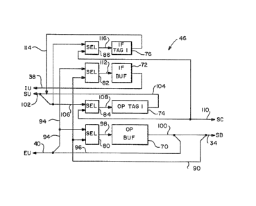
Referring now to Figure 2, the data paths and princi-
pal elements of the split cache 46 are shown. A memory
line destined for the operand buffer 70 is received from
the CPU memory line data bus 34 onto an internal memory
line input bus 90 as one of two inputs to a selector 80. A
second input to the selector 80 is from the execution unit
16 via the CPU-internal operand bus 40 and operand return
bus 94. Upon receiving a systPm controller memory line
move-in request, the cache controller 50 further provides
the IF/OP selection, tag index and memory line associativi
ty of the move-in request to the instruction and operand
buffers 70, 72 to select a unique memory line destination
storage location. That is, if the IF/OP selection made by
the move-in request specifie~ that the memory line provided
onto the internal memory line input bus 90 is destined ~or
the operand buffer 70, the cache controller 50 configures
the selector 80 to pass the memory line data present on the
memory line inpu~ bus 90 to the operand buffer ~0 via the
GBR~AMDH04 -~4- 10/17/86-11
Atty Docket No: AMDH5159DEL/GBR
" ~91)~36~
selector output bus 98. For an instruction buffer destined
memory line, the cache controller will instead configure a
selector 82 to pass the memory line to the instruction
buffer 72 via the selector output data bus 112 for storage
in the tag index and associativity designated storage
location.
During the fourth and final memory line transfer cycle
of the move in, the cache controller further configures one
or both of the Tag 1 selectors 84, 86 for the updating of
the instruction and operand address tags. The necessary
Tag 1 update information is pro~id~d by the system control-
ler as part of the system con~roller mo~e-in request via
control lines 110 (a subset of the system contr~ller
control lines 26). Specifically, the choice to configure
both selectors 84 for address tag access is based on the
create line pair bit of the system controller move-in
request. The system address, public/private, tag valid and
line pair related tag update information is received from
the system controller 20 by the selectors 84, 86 for their
respective instruction and operand Tag 1 buffers 74, 76.
The storage location of the address tags to be updated is
obtained by the cache controller 50 from the system con-
troller 20 move-in request provided information and applied
to the selection of a memory line storage location in the
instruction and operand buffers 70, 72. The address tags
thus written, if for a line pair, are largely identical,
though differing in that they are written with complimenta- -
ry information identi~ying the location of their pair
member location in the instruction or operand buffers 70,
72.
The split cache 46 supports the reading of partial
memory lines (double word) from the instruction buffer 72
in response to an instruction fetch request by the instruc-
tion unit 14. Similarly, partial memory lines are trans-
ferred to or from the operand buf~er 70 either as part of a
memory line move-out or the transfer of operands to the
GBR/AMDH04 -25- 10/17/86-11
Atty Docket No: AMDH5159DEL/GBR
- 1 290~3G~
execution unit 16. For an instrution fetch, the requested
instruction is extracted from the partial instruction
memory line as obtained from the instruction buffer 72,
aligned and then provided to the inst~uction unit 14 via
the CPU-internal instruction bus 38. For a memory line
move-out, the operand buffer 70 acts as a source of four
16 byte data trans~ers occ~rring in four data transfer
cycles. The cache controller 50 effectively transfers the
quarter-memory line seyments ont~ the CPU memory line data
bus 34 by way of the operand ~uffer output data bus 100.
Conversely, where operands are being read from the operand
buffer 70 to the execution unit 16, double word operands
are transferred onto the CPU-internal data bus 40 via the
operand output data bus 96.
With the return of operands from the execution unit
16, the cache controller performs an update operation on
the address tag corresponding to the operand data returned
to the operand buffer 70. That is, the selector 84 is
configured by the cache controller to pass address tag
update information provided by the cache controller, via
cache control tag lines 102, to an input 106 of the selec-
tor 84 at the same time the execution unit operand data is
returned to the operand buffer 70. The operand memory line
Tag l address tag is generally updated simply to mark the
memory line recei~ing the operand as having been modified.
In accordance with the present invention, operands
ori~inated or modified by the execution unit 16 may also be
written back to the instruction buffer 72 at the same time
they are written into the operand buffer 70. Normally,
only complete memory lines are written into the instruction
buffer 72 in response to an instruction memory line move-in
request issued to the system controller 20. However, where
a line pair exists ln the split cache 46 and the operand
buffer member is written to with operand data from the
execution unit 16, the present invention provides for the
instruction buffer resident member of the line pair to be
GBR/AMDH04 -26- lO/17/86-ll
Atty Docket No: AMDH5159DEL/GBR
~9~
equivalently modified. Accordingly, the cache controller
50 configure~ the selector 82 to write modified operand
data to a ~emory line pair member present in the instruc-
tion buf~er 72 simultaneous with th~ writing of the sam~
operand data to the corresponding memory line pair member
in the operand buffer 70. As before, the cache controller
updates the corresponding memory line address tag
present in the op~rand Tag 1 buff r 74 to indicate the
modified status of the operand memory line. The address
tag of an instruction memory line of a line pair need not
be correspondingly accessed, since the Tag 1 modifi~d data
bit for an instruction memory line is not defined and no
other address tag information need bs updated.
In the preferred embodiment of the present invention,
the operand data lines 94' are limited data width such that
only operands that are less than 8 bytes wide or 8 bytes
hal~ word aligned can be written from the execution unit 16
to a memory line stored in the in~truction buffer 72.
Execution unit operands of up to 32 bytes, aligned or
unaligned, can be written to a memory line in the operand
buff0r 70. Where an operand returned by the execution unit
16 is not capable G~ being written into the instruction
buffer 72 via data bus lines 94', the cache controller 50
instead invalidates the instruction buffer line pair member
during the otherwise normal update acce~s o~ the instruc-
tion Tag 1 buffer 75~ The update operation performed on
the address tag of the operand Tag 1 buffer 74 to change
the state o~ the modified bit will further reset the
operand IF/OP line pair state bit if the instruction line
pair member is invalidated. Thus, the line state pair
status is e~fectively destroyed and the instruction line
pair member invalidated, though the operand mamory line
continues to validly exist in the operand buffer 70.
An opexand store invalidation of the instruction Tag 1
address tag without any notice to the system controller ~O,
however, creates the potential for a line pair inaccuracy
G~R/AMDX04 -27- 10/17/86-11
Atty Docket No: AMDH5159DEL/GBR
to subsequently occur as between the instruction and
operand Tag 1 address tags. Such a condition is defined as
a ghost line pair state. That is, the operand address tag
will reference a nonexistent or ghost instruction address
tag as a mutual member of a line pair.
This ghost line pair ~tate can arise if the system
controller 20 moves-in the operand line pair member after
an operand store invalidation of the line pair companion
memory, but without an intervening operand Tag 1 address
tag invalidation or move in into the instruction buffer 72
at ~he instruction line pair tag index and associativity.
Following the instruction address tag inv~lidation, another
CPU 12' must request the operand memory line with only
public privileges and the system controller 20 must only
update the operand Tag 1 addr~ss tag as now being held
public. The operand memory line must then be requested
back by the CPU ~2, again with private privileges. In
making the required move-in, based on the contents of the
Tag 2 buffer 60, the system controller 20 will perform a
short move-in updating the Tag 1 address tags of both the
still invalid instruction and operand memory lines to
indicate that they are mutual members of a line pair. No
check is made as to wheth~r the instruction Tag 1 address
tag is marked invalid. However, this seeming error in the
management of line pair states does not resu~t in any
degradation of the operation of the split cache 46. The
instruction and operand Tag 1 ~uffers 74, 76 remain accu-
rate with respect to the memory lines contained in the
respective instruction and operand memory line buffer~ 70,
72. That is, rP-quests for instructions or operands by the
instruction and execution units 14, 1~ are handled by th~
storage unit 18 based on respective cache controller
searches of the instruction and operand tag 1 buffers 74,
76. Such cache controller searches do depend on the Tag 1
address tag valid bit and are therefore independent of the
presance of a ghost line state.
GBR/AMDH04 ~28 10/17/B6-11
Atty Docket No: AMDH5159DEL/GBR
~2~
The ghost state is tolerated even where the remaining
valid operand memory line of the ghost line pair is again
accessed for the storage of an execution unit modified
operand. The modified operand is, as before, simultane
ously written to the memory line m~mber in th2 instruction
buffer 72, even though it exists as a ghost. This blind
update ~f the instruction Tag 1 buffer is a consequence of
the line pair marked address tag present in the operand Tag
1 buffer 74 indicating the presence of the instruction
memory line member of the pair. The cache co~troller 50
does not update the address tag o~ the invalid memory line
present in the instruction buffer 72 where the store ~f the
operand data to the instruction buffer 72 is possible.
Where the operand instruction buffer store cannot be made
due to the instruction buffer access limitation of the data
bus 94', the subsequent access of the instruction Tag 1
buffer 96 merely inYalidates the already invalid instruc-
tion buffer address tag.
Notably, the ghost member of a ghost line pair is
always invalid. If an instruction memory line move-in
request is completed with respect to the same tag index
instruction storage location as the ghost, a valid line
will exist there. The moved-in memory line can b~ either
the same memory line as the ghost memory line or another
memory line having the same tag index. If the memory line
is the same as the ghost, then the line pair validly
exists. Subsequent operand writes to an instruction line
pair member are proper. Con~-ersely, if a different memory
line is moved-in, then the line pair bit of the operand
address tag will have been corrected during the swap
move-out process invoked in response to the instruction
move-in request. That is, the original move-in request
identifies the ghost instruction memory line for swap
move-out, independent of the line being invalid. The
system controller 20 responds by requesting the instruction
mo~e-out, including the identification of the ghost memory
line as a member of a line pair. As before, the cache
GBR/AMDH04 -29- 10/17/86-ll
Atty Docket No AMDH5159DEL/GBR
~2~30~6~L
controller simply invalidates the instruction memory line
by an update of its instruction Tag 1 address tag. Also,
based on the l~ne pair identification of the swap move-out
line, the operand Tag 1 address tag is accessed specifical-
ly to reset the operand address tag line pair bit.
Thus, a computer system architectllre including multi-
ple CPUs with split instruction and operand caches and
allowing for the simultaneous existence of otherwise
identical memory lines in both the instruction and operand
caches of a single CPU managed through the implementation
of a line pair state for each identical pair o~ memory
lines, has been described.
In light of the above teachings, many modifications
and variations of the present invention are possibla. It
is therefore to be understood that within the scope of the
appended claims, the invention ~ay be practiced otherwise
than as specifically described above.
GBR/AMDH04 -30- 10~17/86-11
Atty Doc~et No: AMDH5159DEL/GBR