Note: Descriptions are shown in the official language in which they were submitted.
AUTO RESET CIRCUIT BREAK~.R
FI~LD OF THE INV~NTION
The present invention is an over-current and/or
over-voltage protection device for use in an electrical
circuit.
BACKGROUND O~ THE INVENTION
... . _
Over-current protection is traditionally provided by
fuses or circuit breakers which require thermal or electro-
magnetic delay intervals for operation. Prior artover-voltage protectors generally are not capable of handling
heavy current. Thus, a need exists for an over-current
protector ~hich provides instantaneous over-current
protection, and which will augment or work in cooperation
with an over-voltage detector to protect both the circuit and
over-voltage device against high-current surges.
The present invention provides the following
advantages over current state of the art devices;
(a) it provides instan-taneous protection at an
electronic speed for the protected circuit, unlike the prior
art devices which are inherently limited to thermal or
electro magnetic delays;
(b) i-t additionally provides over-voltage
protection, providing isolation for the equipment or the
protected line from -the source until the over-vol-tage
condition has subsided;
(c) both the over-curren-t and the over-voltage
protection is fully automatic and does not need to be
manually reset. The device periodically samples the source
3 and load and continues to interrupt the primary line until
the over-voltage or over-current condition has subsided.
'~''
1 The present invention is particularly applicable
and useful for a wide variety of electrical applications, and
may be provided as an AC circuit breaker, a DC circuit
breaker, or an AC-DC circuit breaker.
The ~C circuit version is particularly applicable
to household and industrial application, particularly where
large industrial motors or transformers are involved.
The DC circuit version is particularly applicable
to automotive applications and industrial power supplies for
computers and other voltage sensi-tive DC circuits.
The ~C-DC circuits are particularly useful for the
telecommunications industry, and power companies as surge
protectors used to protect telecommunication lines and AC
lines against lightning surges or other uncontrolled voltage
and/or current-overloads.
SUMMARY OF THE INVENTION
. .
The presen-t invention provides an auto-reset
circuit breaker ~or interrupting an electrical current in a
line or circuit to be protected when the current or voltage
2 exceeds a predetermined value. The circuit breaker includes
at least one solid state silicon switch that is series
mounted in the line of the circuit to be protec-ted. This
switch is responsive to a first control signal to open the
switch to interrupt the current flow~ng therethrough. The
circuit breaker includes a first means for measuring a
variable voltage drop across at least one element series
mounted in the line to be protected, which may be a resistor,
a resistor network, or -the switch itself. This ~irst means
generates a trip signal when the voltage drop across the
series element and the electrical curren-t in the line to be
protec-ted exceed predetermlned values. ~ second means is
~5
~' .
. I
_ 3 ~ 7
1 provided that is responsive to the trip signal for providing
a first control signal to the silicon switch, wherein the
control~signal is effective to open the switch when the
electrical current has exceeded the predetermined value. A
delay means is also provided that is responsive to the trip
signal for enabling the second means for a delay interval,
whereby the electrical current is periodically reestablished
and then broken at each delay interval until the electrical
current and the trip voltage drop below their predetermined
values.
The second means of the presen-t invention may be
programmed to select any one of a plurality of predetermined
values for the trip signal voltage. In addition, the series
element in the line to be protected may comprise a resistor
network having a plurality of values to provide surge current
protection at a variety of predetermined levels.
The auto-reset circuit breaker oE the present
invention, may also be rendered in diyital form with an
analog to digital converter measuring the voltage across the
solid state switch and converting the analog voltage to
digital form. A comparator is then provided to trigger the
solid state switch or the second control means when a
predetermined voltage drop has been exceeded.
The solid state switch of -the present invention may
be a triac, an SCR, or a pair of complimentary ~p & n or n & n)
field effect transistors.
The auto-reset circuit breaker of the present
invention may also be used in combination with a high volta~e
and current primary protection device which is mounted
between -the line to be protec-ted and earthground, with the
3o
primary protection device connected in fron-t of the solid
-4~
gate switch. A transient voltage suppressor may also be
mounted between each of the line to be protected and ground
with the transient suppressor connected behind the solid
state switch. In addition, the auto-reset circuit breaker of
the present invention may be connected in a multi-line
environment to provide over-current protection between each
of the lines and between each of the lines and ground.
BRIEF DESCRIPTION OF THE DRAWINGS
.. . .
Figure 1 is block diagram illustrating the
functional relationship of the various components of the
present invention, and the components to be used if the
invention is to be rendered in digital form~
Figure l(a) illustrates an over-current condition
on line 12, 14.
Figure l(b) illustra-tes the signal present at the
input to the solid state switch illustrated in Figure 1.
Figure l(c) illustrates the output signal at 25 of
the control circuit illustra-ted in Figure 1.
Figure l(d) illustrates the outpu-t of the time
2 delay circuit illustrated in Figure 1.
Figure 2 illustrates the circuit of the present
invention when rendered in analog form with conventional
components.
Figure 3 illustrates an improved embodiment of the
present invention adding a gate amplified circuit.
Figure 4 illustrates an embodiment o~ the present
invention par-t.cularly adapted ~or use in a DC environment.
Figure 5 is a diagrama-tic illustration of the
present invention adapted for use in a novel pyramid
protector intended for use in telecommunication lines and AC
line feeds.
~ .
~,2.~
l Figure 6 is a schematic illustration of the present
invention when used in the pyramicl protector illustrated in
Figure 5.
Fi~ure 6(a) is a schematic illustration of an
alterna-tive form o~ -transient voltage protection for the
circuit illustrated in Figure 6.
Figure 7 is a graph illustrating the response o~
conventional devices and the pyramid protector to an
over-voltage condition.
Figure 8 is an illustration of improvement offered
by the present invention with respect to "gray area" voltage
and current conditions.
Figure 9 is a schematic illustration of the
preferred embodiment of the present invention, particularly
adapted for use in the pyramid protector as an ~C-DC circuit.
~ igure 10 is a schema-tic illustration of the
present invention in a bidirectional multi-line environment
using a diode bridge recti~ier.
DETAILED DESCRIPTION OF THE INVENTION
. . _ .
~ he over-current/over-voltage auto-reset circuit
breaker of the present invention is illustrated in the Block
diagram of E'igure 1. The auto-reset circuit breaker 10 is
normally connec-ted in series to an electrical circuit 12, 14
to be protected, in place o~, or in addition to an ordinary
fuse or circuit breaker. The return leg o~ the circuit in
Pigure l is illustrated as 12', 14'. The presen-t invention
may be used in a conventional 2 line AC or DC circuit as
illustrated, or may be installed in a DC environment wherein
12', 1~' is a chassis ground. Other applications oE the
circuit will be herea~ter described, and will be appaxent to
those skilled in the art.
,,~
_~ 6
l The auto-reset device lO includes a solid state
switch 16 which is biased to be normally closed. A current
detection means 15 consisting of a series resistor 18 (also
known as a shunt resistor), generates a voltage drop across
it, which is proportional to the current flowing therethrough
on line 12, 14. This voltage drop is proportional to the
value of its resistance. In normal operation, the resistor
18 has an extremely low value, which may be on the order of
.5 ohms for a 110-220V AC circuit. This voltage drop may
then be converted to a digital value by the analog to digital
converter 23. When the current through the line 12, 14 and
resistor 18 exceeds the designed current, the voltage drop
across 20,21 and the digital value at 24, will trigger the
control circuit 22. Control circuit 22 is a compara-tor which
will compare the the incoming signal of 24 with a preset
value. When the trip signal voltage at 24 exceeds that
value, the comparator control circuit will produce a low
going first control signal at 25 (illus-trated a-t Figure l(c)l
which opens the solid state switch 16 through AN~ gate 30~
Simultaneously, the ~irst low input signal at 25
also initiates a time delay means 26, which also goes low as
indicated in Figure l(d) to hold the AND gate 30 in a low
position until the end of the delay period. Swi~ch 16 is
thereby held open through the entire delay period as
indicated at l(b). ~t the end of the delay period, the
output of 30 is high, and if the ~irst control signal is also
high at 25, the AND gate will be reset to close switch 16.
If the first control signal at 25 is still low, due to a
continuing short or o-ther overcurrent condi-tion on the line,
the time delay 26 will be reset for another delay interval.
3o
.~
~'9~7
l Thus, as seen from the Figures l~a~ through Figure
l(d), each time the current in the circuit exceeds a
predetermined design current the solid state switch 16 opens
for a predetermined time period, thus instantaneously
disrupting tlle flow of the over-current, but automatically
resetting at the end of the predetermined time delay.
Additionally, the circuit 10 also includes an
over-voltage trip signal detector 34. Thus, upon detection
of an over-voltage condition across the line 12, 12' the
over-voltage detector 34 automatically triggers the control
circuit 22 to shut off the solid solid state switch 16 as
described previously, until -the over-voltage condition has
subsided, t~us preventing any over-voltage from reaching the
protected line. The measurement o~ the over-voltage may be
done by the over volta~e detector 34 by measuring across the
line 12, 12' as indicated at 35, 36 or alternative may be
installed across the switch 16 via 35, 37 to measure the
over-voltage when the switch 16 is open. In the latter form,
over-voltage protection can be provided in a single series
element device, without reference to line 12' 14' or ground.
The series resistor 18 may also be a resistor
network, or may be programmable such that different taps may
be used to set the limiting current value of the circuit.
Alternatively, the control circuit's trip signal voltage
threshold at 24 may be modified to se-t the limiting current.
In a digital device, this may be done via software
controlling the trip voltage threshold, thus allowing ~or
programmability of the circuit in the form of nonvolatile
~emory, even after the hardware has been build.
3o
l The series resistor 18 ~ay be eliminated by
monitoring the voltage across the solid state silicon switch
16. When the triac is used for switch 16, a small voltage
drop, on the order of .7V is present across the switch. This
voltage drop will ramp upwardly in a linear manner as current
through the triac increases. This increase, when converted
to digital format, may be used to trigger the control circuit
22.
In the above example, the programming may be done at
factory to meet the current needs, or the units may be field
programmed, ~hus allowing maximum flexibility to the user o~
the device.
Unlike the prior art fuses and circuit breakers,
which operate on thermal or magnetic principles, the
auto-reset circuit hreaker operates at an electronic speed
hich far exceeds any thermal or magnetic breaker. Thus,
there is never any heat generated in the protected circuit,
due to any over-curren-t, since the solid state switch 16
opens instantaneously thus avoiding any form o~ heat buildup
in any components of the protected electrical circuit.
Figure 1 has been used to illustrate the present
invention at the conceptual level and as a digital device.
Figure 2 illustrates the presen-t invention in an analog
circuit using a minimum number oE components.
As illustrated in Figure 2, the present invention
is series connected in an AC line 12,14 to be protected.
Triac 40 forms the solid state switch 16 illustrated in
Figure 1. While a triac is normally open, the switch 16 is
closed in an ~C environmen-t by a bias resis-tor 46 which feeds
0 the gate, as indicated at 44, to -turn the triac on at the
3 beginning of each half-cycle of ~C current. The triac 40 is
.~
9 $ ~ 1[3~
1 turned o~, or opened by a second triac 48 which shorts the
gate of triac 40 ~o the line at 14. The ~irst control signal
discussecl previously is the absence o~ a gate voltage for
triac 40, which would otherwise be available Erom resistor
46. Triac 48 is responsive to the trip signal discussed
previousl~ to disable triac 40, and thus open the switch 16.
When the gate 44 is shorted, the triac ~0 will remain on for
the remainder o~ the AC half-cycle, but will be prevented
from firing or closing during the next half-cycle.
The over-current condition is detected by measuring
the voltage drop across series resistor 18. .Depending on the
AC half-cycle and the polarity of -this voltage at 42, either
diode 58 or diode 60 will conduct and charge the its
associated intergrating capacitor 54 or 56 respectively.
Capacitors 59, 56 thereby form a first means for measuring
the voltage drop across the series resistor 18, with the
voltage drop proportional to the current in the protective
line 12, 14. ~ trip signal is generated when the intergrated
voltage present in either capacitor 54 or 56 is suf~icient
to forward bias its associated schottky diode 62 or 64 , and
trigger the triac 48. The trip signal or trigger voltage is
a predetermined value which is the sum of the gate turn on
voltage for triac 48 and the breakover voltage for the
schottky diode 62, 64. Schottky diodes are preferred for
this application since they provide a low forward voltage
drop which renders the trigger circuit more sensitive. Thus,
a smaller resis-tor value may be used Eor resistor 18. In a
typical llOV ~C line environment, protected for 20 amperes,
the resistor 18 would be 0~055 ohms and would generate a
voltage drop oE l.lV when 20 amperes is reached. The gate
turn on voltage for the triac is 0.7V, and the breakover or
' ;~
~,2~
l trigger voltage for schottky diode 62, 64 would be 0.4V. The
combined voltage forms a trip signal for the circuit and is
predetermined by the appropriate selection the component
values for resistor 18 and diodes 62, 64.
A delay means, responsive to the value of the trip
signal is provided by the time constant of the decay of
capacitors 54, 56 through resistor 66. The delay period is
proportional to the value of -the trip signal voltage in
capacitors 54, 56 which is in turn proportional to the value
1 of the surge current passing through resistor 18. Thus, if
the surge current was such that the off delay capacitors were
sufficiently charged to keep control triac 48 on for several
subsequent cycles, the triac 40 (switch 16) will remain off
for that time period, preventing any flow o~ current to the
equipment or protected line, except that which passes through
resistor 46.
As the voltage across the off delay capacitors 54,
56 decays, below the gate trigger vol-ta~e for control triac
48, the second triac means 48 is disabled and triac 40 is
again permitted to turn on through the bias resistor 46. If
the current at this time should be again greater than the
prese-t limit, the above described events will be repeated
.until the current in the protected circuit falls below the
nominal value preselected for that particular circuit
application.
Intrinsic to the foregoing operation is a zero
crossing turn on or turn of~ mechanism~ The term zero
crossing refers to the AC line voltage crossing zero on
conductor 12, 14. A typical triac, once turned on, will
remain on until the current in the clrcuit drops to below the
3 triac holding current. This constitutes the zero crossing
'~
1 -turn off. At each zero crossing, if the control triac 48 is
on, i-t will be latched on for the entire half of that cycle
until the current goes to zero again, at which point only if
the control triac 48 is not gated on, will the triac ~0 be
permitted to turn on, thus providing a much desired feature,
a zero crossing turn on. This is particularly desirable for
use in any AC inductive circui-t, such as AC transformers,
relays, motors or the like.
The circuit illustrated in Figure 2, is
particularly useful in an AC environment. It may be adapted
for a DC environment by replacing triac 40 with a gate turn
off triac. A normal triac remains conductive, once turned on
regardless of the ga-te voltage, until the current in the
circuit drops below the holding current of the triac. Thus a
normal triac cannot be used as a swi-tch in a DC environment,
since it would stay on after the device has been triggered
on. However, a GTO-triac will cease to conduct at the instant
the gate control voltage is removed or shorted out. Thus,
the circuit of Figure 2, when equipped with a GTO-triac in
2 :Lieu of triac 40, may be used in a DC environment. By using
a GTO-triac, one loses -the zero crossing turn off for an AC
environment, but gains the ability to use the circuit in an
AC, DC or AC-DC line environment.
It should also be noted that the voltage drop for
the trip signal could also be measured by measuring the
voltage drop across the triac ~0 in lieu of resistor 18. The
voltage drop across the switch would be proportional to -the
amount of current flowing through the protected circuit. As
indicated in Figure 1, this may be monitored by an analog to
digital converter and comparator to compare the instantaneous
3 digital reading to a preset digital setting. Should the
~,
-12~
instantaneOuS reading exceed the preset limit, then the
control triac 4~ would be turned on as described previously,
which will in turn short the gate of triac 40 and turn switch
16 off for the required time delay.
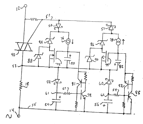
Figure 3 is a more elaborate version of the circuit
of Figure 2, wherein the gate trigger resistor 46 is replaced
with a pair of FETs w~lich provide a full maximum gate trigger
current for the triac 40. The gate trigger resistor 46
illustrated in Figure 2, must deliver sufficient gate current
O to enable the triac 40 in the normal operational mode, and
yet be able to handle all of the voltage imposed across it
when the triac 40 is in the open sta-te due to an overload
condition. This requires that the ga-te trigger resistor 46
be low in value for the sake of delivering sufficient gate
trigger current, and also have a high voltage and power
rating in order to handle all of the power across it, when
the control triac 48 has been turned on, and triac 40 has
been turned off. This results in a heavy and bulky resistor
~1hich may be avoided by the use o~ FETs 72 and 74 as
2 illustrated in the gate amplified circuit of Figure 3.
As illustrated in Figure 3, the gate turn on
resistor 44 is replaced by a pair o:E constant current devices
76, 78 and matching FETs 72, 74 which provide a gate trigger
current Eor the triac 40.
When 53 is negative, FET 72 is turned o~ by a
voltage across capacitor 80. Once conductive, FET 72
establislles the gate turn on current for triac 40 at 52
through the zener diode 84 and schottky diode 50. Whe~n 14,
53 goes positive, FET 74 .is turned on by the voltage across
capacitor 82. Once conductive, FET 74 establishes the gate
turn on current for triac 40 through zener diode 86 and
schottky diocle 51.
,,, ~ .
-13~ "~
1 The current carried by the switch, and the voltage
drop across resistor 18 is measured by intergrating
capacitors S4, 56 which are charged in their respective
polarities by schot-tky diodes 58, 60.
When an over-current condition is encountered, the
trip voltage a-t 61 or 62 (depending on the line polarity)
will render the latching transistor pair 79, 81 or 83, 85
conductive. Alternately, an SCR may be used in lieu of 79,
81 with a second SCR replacing pair 83, 85. As illustrated,
the latching transistor pairs are regenerative and once
triggered, remain latched as long as the trigger voltage is
present on capacitors 54, 56.
When the trip voltage is reached at 61, transistor
79 is rendered conductive which renders transistor 81
conductive to short the capacitor 80 to ground and prevent
the constant current device 76 from turning FET 72 on. With
FET 72 off, there is no ga-te current at 52 to turn on triac
40. As long as the transistor pair 79, 81 remain latched,
any current through the constant current device will be
shorted through transistor 80 to line 55.
The transistor pair 79, 81 will remain latched
until the voltage stored on capacitor 54 is discharged by
resistor 57 to rail 55. The operation of capacitor 56,
transistor pair 83, 85, capacitor 82 and constant current
device 78 is identical, but uperab:le in the opposite
half-cycle when 53 goes nega-tive.
When the transistor pairs 79, 81 and 83, 85 are
unlatched, then the appropriate FET, 72 or 74, will close the
triac 40 on the next zero crossirg. If the over-current
condition still exists, then the trigger and delay cycle is
3o
repeated.
-14-
1 The delay means of Figure 3 includes both of the
capacitor pairs, including capacitors 54, 80 for one polarity
and capacitors 56, ~2 for the other polarity. The capacitor
pair 54, being discharyed through resistor 57 and transistor
pair 79, 81 and capacitor pair 56, 81 being discharged
through resistor 59 and capacitor pair 83, 85.
Zener diodes 84, 86 provide a small voltage stand
off to enable the transistor pairs to latch during
over-current conditions before the triac 40 can be triggered.
Zener diodes 88, 90 provide over~voltage protection for the
FETs 72 and 74.
Figure 4 illustrates an auto-reset circuit breaker
particularly adapted for use in a DC circuit as a two element
device. The phrase two element means that the device works
off the line power while being in series (2 terminal
arrangement) with the circuit. As a DC device, the circuit
of Figure 4 needs to be properly polarized when connected to
the DC circuit. Terminal 100 is the positive end of the
device and is connected to the positive end of the line to be
2 protected, while terminal 102 is the negative terminal of the
device and is connected to the negative end of the line to be
protected.
Transistor 104 is used as the solid state switch 16
of this circuit. During normal use, transistor 104 is biased
t:o a conductive sta~e by means of the vol-tage differential
across a gate turn on resistor 106.
Resistor 18 is used to moni-tor the current flow and
generate the trip vol-tage in the circuit in the event of a
current surge. The trip voltage for the circuit of Figure 4
being the sum of the forward biasing voltage for schottky diode
110 and the gate turn-on voltage for SC~ 114. Capacitor 108
'1~,,
-15-
l integrates or "measures" the voltage drop across the resistor
18, and when an over-current condition occurs, the voltage
drop across resistor 18 triggers -the SCR 114. When the SCR
114 is triggered, or turned on, the gate turn-on current
developed by resistor 106 will be shorted to the line 102,
and transistor 104 will cea~e to conduct.
Since there is no holding or latching current for
SCR 114, the transistor 104 will be held open only for the
period o~ time that the gate trigger current at 120 exceeds
0 the gate trigger current developed by resistor 116. This
condition is determined by the time delay capacitor 108 and
resistor 116. The delay interval exists until capacitor 108
is discharged below the trip voltage level determined ~y
SCR 120. A-t this point the SCR ceases to conduct, and gate
turn-resistor 106 biases again, the transistor 104 to a
conductive state.
If the over-current condition continues to exist,
the voltage drop across resistor 18 will recharge capacitor
108 to develop -the trip signal for the control SCR 114~ The
flrst control signal then shunts the gate current for
transistor 104, thereby opening the circuit and protecting the
line 100, 102 from the over-current condition. This novel
reset feature will continue to be repeated at the delay
inter~al determined by capacitor 10~ and resistor 116 and
capacitor 108 until the over-current condition subsides.
Figure 5 illustrates a new kind of lightning and
over-current, over-voltage protector appl.icable to multiple
line circuits. Applicant has termed this de~ice a "Pyramid
Protector". Figure 5 is a diagramatic illustration of a tw~
line pyramid protec-tor. All two line circui-ts, and
particularly those in the -telecommunication and computer
industry are subject to lightning surges and strikes.
~'
.~,,
- -16- ~ t7
l Lightning spilces and surges are particularly harmful to the
electronlcs associated with these industries, and the pyramid
protector is particularly useful as a point of entry
protection device at both the network level and tlle
individual equipment level.
Each line is equipped with a line to line and line
to ground primary lightning protector for shunting
over-voltage surges with a high energy content. As
illustrated in the block diagram of Figure 5, a primary gas
tube or similar type of surge arrester is mounted across the
line from A to B and Ground, providing primary lightning
protection between 130, 132 and 134. This is illustrated by
the triangle A-B-G in the base of the pyramid in Figure 5.
The output of the pyramid protector is connected
across A', B' and ground and is normally a secondary three
element transient voltage suppressor protecting the equipment
side of the protector. This is represented by the triangle
formed by A', B' and G.
,The inputs are connected to the outputs with two
AC/DC auto reset circuits as will be hereafter described with
respect to Figure 9. The pair of auto reset breakers A - A'
and B - B', connect the primary protector to the secondary
protector. Each auto reset breaker has dual mode of
operation. Both over-current be-tween 130-136 and/or
132-138 respectively, or over-voltage from line to line in
each leg 130-136 and/or 132-138 and/or 130-132 and/or 136-138
andlor 136-138 and/or 138-134 from line to ground will open
the auto-r~set breaker. This separates the primary protector
from the secondary protector, and the primary protector is
then permitted to see the antire incoming surge voltage
3 without being impeded by the clamping o~ the secondary
transient volt~ge suppressor.
1~,
--17--
~J~
1 Thus, -the secondar~ protector always remains across
the output of the protector and the input of the equipment it
protects. The series connected auto-reset circuit breakers
continue to isolate the input from the output, as long as
over-current and/or over-voltage condition exists. The
primary protector in the example may be compared to a
work-horse due to its ability to handle large energy surges.
The secondary protector is analogous to a race-horse, since
its speed enables it to handle very fast incoming surges.
Thus, as seen from Figure 5, over-voltage/over-
current protection is provided along each side of the
pyramid, hence the name pyramid protector.
The circuit diagram of Figure 6 is a schematic
illustration of the block diagram of Figure 5.
A three element gas tube arrester 140 connects
across the incoming lines 130, 132 and ground 134.
~ uto-reset AC/DC circuit breakers 10 and 10'
connect across 130, 136 and 132, 138 respectivel~. They
remain in a normally closed posi-tion until an over-current or
over-voltage condition is detected.
Diodes 146 thru 156 form a secondary protector 159
which uses a three phase bridge rectifier requiring only one
transient voltage suppressor 155 to be across the positive
157, and negative 158 ends, of the bridge. This novel
arrangement maintains a true 3 pole, three element ga5 tube,
like characteristics wherein all voltages line to line or
line to ground are kept to the same po-tential, as determined
by the transient voltage suppressor 155. This ensures that
the voltage across -the output, i.e., to the equipment, never
3o
~5
,~.
-18~
1 exceeds the prescribed limit. The use of the bridge
rectifier also reduces the number of transient suppressors
normally required for line -to line and line to ground
protectiOn, thus providing a more economical circuit for the
same level of protection.
Figure 6(a) illustrates an alternate form of
transient voltage suppressor that may be installed in the
circuit illustrated in Figure 6 in lieu of the transient
suppressor 155. This improvement enables the transient
suppressor network to function at sub-nano second speed
characteristic of a Zener diode, with the power handling
capability of an SCR. Low voltage, high power Zener diodes
are readily available, and high voltage, low power Zener
diodes are readily available but high voltage, high power
zener diodes are very expensive. The circuit of Figure 6(a)
combines a high voltage low power Zener 159 and a low voltage
high power Zener 160 in series to achieve a fast response
time in the sub nano second range. The SCR 162 is switched
in after a voltage spike is encountered -to protect Zener 159
from a high energy load, and to fold back the break-over
voltage of the combined circuit to prevent a runaway
condition. When a single Zener encounters a high voltage
spike, the spike is not always limited to the Zener vol~age,
since the voltage will continue to ramp up as the current
dissipated by the Zener increases. The fold back ~eature ~
Figure 6ta) prevents this runaway condition.
As illustrated in Figure 6(a), Zener 161 breaks
over at a first transient voltage TSl, which may be 300
volts. Zener diode 16Q breaks as a second transient voltage
TS2, which may be 60 volts. When a -transient voltage spike
3 is encountered, -the Zener 159 and 160 will breakover in
3~
-19-
1 series in the sub-nano second speed range. The SCR 162 has a
characteristic delay of 1 to 3 ~s beEore turning on. Zener
159 is able to conduct the voltage and energy for the short 1
to 3/~s duration, even though it might not be able to handle
the entire duration of the spike. After the SCR 162 fires,
the voltage protection will fold back to the 60 volt level
set by Zener 160.
Figure 7 illustrates in graphic form, the action of
the pyramid protector on an incoming voltage surge, wherèin
voltage is the Y-axis, and time is the X axis. In the
absence of any protection, the incoming voltage would
continue to rise along line 164 until the gas tube 140 fires.
As the gas tube 140 fires at 172, the incoming voltage will
drop along the line 166 to a safe voltage corresponding to
the line 168 and remains there until the surge condition has
passed away. The time it takes for the gas tube 140 to fire
can often be sufficient to blow the microelectronic or
integrated circuits in most sensitive telecommunications or
computer equipment. This time period o~ untaimed surge
voltage is reduced by the use of a secondary protector as
formed by the six rectifying diodes 146 thru 154 and the
transient suppressor 155, or the substitute therefore as
shown in Figure 6b.
When the incoming voltage rises to the transient
suppressor breakover voltage 170, the transient suppressor
begins to conduct heavily, which causes the auto-reset
circuit breaker to open the circuit between the input and -the
output thus releaving -the secondary pro-tector 155, as well as
the related equipment across the output, ~rom any sustained
over-voltage or current. ~s illustrated in Figure 7, as the
3 voltage continues to rise beyond 170, -the excess voltage
.~
-20- ~;,?~ 2 ~ ~
1 across the input lines 130, 132 or line to ground 134, will
maintain the auto-reset circuit breaker o~ the pyramid
protector in the open state until the gas tube fires at 172
and the voltage across the input drops to the level shown by
168. The voltage across the output of the pyramid protector
is illustrated with the dotted line 167, which drops to zero
as soon as the transient voltage suppressor 155 ~egins to
conduct. The output of a conventional device, having cnly a
gas tube primary and a transient secondary is illustrated by
the dotted line 169. When only a transient voltage
suppressor is available, the voltage rise will initially
stop, b~t will then begin to rise in a runaway condition as
the current drained by the suppressor increases.
Figure 8 illustrates an additional level of
protection provided by the pyramid protector in the "gray
zone" that exists below the firing point of the primary gas
tube. A conventional gas tube and transient protection
device is particularly vulnerable to an over-voltage
over-current condition -that may exist above the intended
operating voltage, but below the gas tube firing voltage.
Figure 8 illustra-tes a typical gas tube voltage of
approximately 450 volts at 163, and a typical transient
suppressor level of 220 volts at 165. A typical design limit
for a telecommunication environment of 100 millamp at nominal
voltage is indicated at 171. DC voltage curves have been
used in Figure 8 for simplicity of illustration, although,
same pxinciples apply to an ~C voltage, or a com~ined AC/DC
voltage environment. When a volta~e~current within the
design limi-t Vl is encountered, the voltage is handled
normally and the output passes the full volta~e/current to
3 the protected equipment.
'~
-21-
l When an over-voltage V2 :is encountered without the
present invention, the voltage rises until it reaches the
transient suppressor breakover voltage as indicated at 170.
At that point the voltage/current is conducted to ground, but
the voltage continues to ramp up as the current to ground
increases. If the gas tube voltage is not reached, both the
transient suppressor and the protected equipment will "cook"
in the gray area 173 of Figure 8, until the condition is
removed, or until an element fails ~rom the overload.
In contrast, the pyramid protector cuts the voltage
as indicated at Vp as soon as the voltage/current exceeds the
design limit. The breakover point in Figure 7 for the
pyramid protection is illustrated for an over-voltage surge
without a load on the line. Figure 8 illustrates a normal
telecommunications environment with a nominal load. A`delay
interval Dt is designed into the auto-reset circuit breaker.
At the end of the delay in-terval, the pyramid protector will
again begin to conduct as illustrated at Vp2, until the
combined volt~ge/current is reached. This continues until
2 with Vp3, Vp~ ... Vpn until the over-voltage condition ls
removed.
Figure 9 is a schematic diagram of a complete
pyramid protector as described in the circuit diagram o~
Figure 6 with the auto-reset circuit breakers defined in
detail. Figure 9 therefore represents two AC/DC auto-reset
circuit bre~ker elements lO and 10' and the solid state
secondary protector 159 of Figure 6 in a combined device
suitable for IC Eabrica-tion.
Illustrated in Figure 9 are the input5 to the
pyramid protector 130 and 132 which connect to the two
incoming lines of a telecommunications circuit or two lines
from an AC Power Source.
'~
~.~,
-22~ .2~7
1 Lines 136 and 138 constitute the output of the
above two lines exiting from the pyramid protector to the
load being protected.
Connected in series between the inputs 130 and 132,
and the outputs 136 and 138 respectively, are conventional
fuses 222 and 224. Bridged across the outputs 136, 138 is
also connected a three element solid state secondary
protector 159 which responds at electronic speed and has the
fold-back characteristics of an conventional gas tube or
similar spark-gap arrester.
The solid state protector not only monitors the
voltage across the output lines 136, 138 and ground 136, but
also senses the incoming voltage across the input lines 130
and 132 with respect to each other and with respect to ground
via the resistors 226 and 228. The auto reset circuit
breakers 10 and 10' consist o~ series resistors 18 and 18'
and solid state switches 16 and 16' respectively.
Resistor 192 connects across the two solid state
switches 16 and 16' keeping them normally ON or closed.
Also connec-ted across the inputs and the outputs oE the solid
state switches 16 and 16' are solid s-tate over-voltage
protectors 218 and 220 respectively. Upon seeing
over-voltage across the solid s~ate switches 16 and 16' these
go into heavy conduction. In the presen-t illustration a
bilateral over-voltage protector with fold back
characteristics is illustrated.
Under over-voltage conditions the Gas-tube 140 will
operate and put a short across the lines 130 and 132 to
ground 136. ~lowever, during the characteristic ionization
time required by the gas-tube 140, the entire incoming
3 voltage is passed on to the output 136, 138 in the absence o~
the auto-reset circuit breakers 10 and 10'.
,~
~23~ 2~'~
1 The incoming voltage is then clamped at the output
to the restricted level as allowed by the secondary protector
at a sub-nano second electronic speed. Simultaneously the
auto-reset circuit breakers 10 and 10' are triggered by this
over-voltage condition via the aforementioned resistors 226
and 228 and open the normally closed switches 16 and 16'
respectively, In the absence of the resistors 226 and 228,
the secondary protector 159 would clamp the over-voltage and
generate an over-current through the series resistor 18 and
18' which would consequently also open the normally closed
solid state switches 16 and 16' respectively,
The opening of the solid state switches achieves
two purposes, first it isolates the load across 136-138 from
the potentially damaging over-voltage condition at the input,
and secondly it permits the incoming voltage to rise freely
so tha~ it may allow -the primary protector 140 to operate and
shunt all the damaging surge potential -to ground.
In the over-current mode, which may be due to t~e
over-voltage being passed on to -the secondary protector or`a
short or overload being placed across the line 136, 138 with
nominal voltage across the line, the circuit performs the
conventional function of the over-current protec-tor. Should
the current exceed the design limi-t of the device a trip
voltage generated across the series resistors 18 and 18' will
trigger a control circuit to open the normally closed
switches 16, 16'. This interrupts the path o~ the over-
current through the device.
The resistors 194, 194' and the capacitors 214 and
214' form an ON-delay function for tailoring the time
permitted for the over-current to flow through -the circuit
3 beEore the auto-reset circuit breaker interrupts the flow of
over-current.
.. ~ . I
-24- ~d,'~
l Similarly, the resistors l9S and 195' and the
capacitors 214 and 21~ form an off-delay function or
tailoring the delay interval of the auto-reset function of
the circuit.
The gate capacitors 204, 204' and the inter-
connecting feed resistor 192 define an additional delay
interval for the circuit before it automatically resets the
switches 16, 16'.
In the case of sustained over-voltage where the
1 primary protector 140 breakdown voltage is not reached, but
the over-voltage exceeds that of the secondary protector 159,
the auto-reset circuit breaker will remain in the open state.
However, by design the voltage now will be distributed across
the pass element protectors 218 and 220 and across the
secondary protector 159. In the rare event where a current
through the above is sustained -to a ca-tastrophic level the
conventional fuses 222 and 226 respectively will open, thus
preventing permanent damage to the devices or the load.
These conventional fuse elements 222 and 226 may then be
replaced.
The circuit of Figure 9 is bilateral in both legs
130, 136 and 132, 138. The service or input can be either
positive or negative, providing ac, dc or ac/dc capability.
Switches 16, 16' are ~ormed with pairs of
complimentary FET's 180, 182 and 180', 182'. The FET's are
biased on by a voltage divider network extending across the
legs of the pyramid protector, said divider including (from
terminal 130) resistor 18, Zener 190, resistor 192, Zener
190' and resistor 18' (to terminal 132).
When line 130 is positive and line 132 is negative,
3 the gate 188 of the FET switches 180, 182~ will be negative
with respect -to line 130 by virtue of the voltage applied
across voltage divider network. This negative voltage at
~5
..~
t ~ a;`~
-25-
l gate 188, turns on P-FET 180, which establishes a path for a
flow of current from line 130 through resistor 18, diode 186
and P-FET 180 -to the output terminal 136. If a load is
connected across 136 and 138, then the above current will
flow through the load back to 138 continuing through diode
184' and ~ET 182' and resistor 18' to terminal 132. FET 182'
will be biased "ON" due to the positive voltage applied to
its gate 188' as supplied by the previously described voltage
divider network.
The over-current and over-voltage monitoring
circuits, include 4 pairs of latching transistors, with two
pairs associated with each leg to provide bilateral
capability in each leg. Transistors 196, 198 form a latching
configuration when terminal 130 is positive, while
transistors 200, 202 form a latching configuration when
terminal 130 is negative. Likewise, transistors 196', 198'
form a latching pair when terminal 132 is positive, while
transistors 200', 202' form a latching pair when terminal 132
is negative.
Excess current flowing through the current
measuring resistors 18 and/or 18' will generate an excess
voltage drop across them which will be proportional to the
product of current and resistance (Vx = Ix- R) 18 and 18'
respectively.
The voltage drop Erom resis~or 18 is current
limited by resistors 194 and 1~5, and integra-ted by capaci-tor
204. Likewise, either voltage drop across resistor 18' is
current limited by resistors 194' and 195' and in-tegrated by
capacitor 204'. When the voltage drop across resistor 18
exceeds a predetermined level, it biases one o~ the lakching
3 yairs (depending on polarity) 196, 198 or 220, 202 into
conduction.
~"f,,
b
-26~ r~ 7
l Likewise, when the voltage drop across resistor 18'
exceeds a predetermined level, it biases one of the latching
pairs (depending on polarity) 196', 198' or 200', 202' into
conduction. When the latching pairs are conductive, the
junctions 203, 203' are shorted to their respective terminals
130, 132 to discharge the capacitors 204, 204' and remove the
gate voltage from the FET switches r thereby rendering the
~ETs non-conductive and opening the primary circuit (switches
16, 16').
The auto-reset function of Figure 9 is determined
first by the rlc time constant of resistor 195 and capacitor
214 (and resistor 195' and capacitor 214'). Capacitor 214
will keep the latching pair of transistors in conduction
until completely discharged by resistor 194. However, the
FET switch pairs will remain o~ until the voltage divide
network is able to recharge capacitor 204, 204' to the FET
gate turn on voltage. The delay interval is then the sum of
the two delay periods.
In an over-current condi-tion, the circuit will
periodically close the FET pairs to determine if the
over-current condi-tion still exists. In an over-voltage
condition, the transistor pairs will be sustained in the
latched condition from the bias provided by the over-voltage
condition.
The other over-voltage detec-tion feature of this
circuit occurs when excess voltage is on the line, from line
to line or line to ground. Even when the switches 16! 16'
are OFF, the over-voltage is fed to the transieht suppressors
160 and 161 o~ the secondary protector 159 via the resistors
226 and/or 228. The resistors 226 and 228 are very large in
3 volume so that there is only a small amount oE current that
.~ ;
~
-27-
1 flows through the base emitter junctions of the latching
transistor pairs in the appropriate polarity. Yet it is
enough to keep the latch turned on even wi-th only slight
over-voltage condition, thus keeping the FET switches OFF
even when there is no excess current condition, or no load
connected across the output 136, 138. Diodes 230 and 234
rectify the line voltage from line 130 via resistor 226,
while Diodes 232 and 236 rectify the line voltage from line
132 via resistor 228.
Thus, the latching pairs are responsive to either
on over-current or on over-voltage condition to keep the FET
pairs non-conductive and the s~7itches 16, 16' open.
During the time the FET switches are open, the
circuit is open, which permits the full input voltage to
1 appear across the line 130-132, without being shunted by the
circuit in any wayr thus allowing the primary protector 140,
or a comparable protector such as a spark gap device, to
break down and shunt the entire surge current. Should the
surge continue to rise, or the gas tube 140 ~ails to ionize,
the incoming voltage will be divided across the transient
suppressor network. This network includes a diode bridge
146, 148, 152 and 154 connected across the rails 130, 136 and
132, 138. The diode bridge is also connected to ground
through diodes 150 and 156. The transient suppressor
previously described with respect to Figure 6 is placed
across the bridge to conduct to ground in the event a ~oltage
transient is received. A short transient, which is shorter
than the "on" delay o~ capacitors 214, 214', will pass
through the FET pairs, bu-t will be grounded by the transient
suppressor network.
3o
-2B-
l The output voltage is also protected by the bridge
circuit protecting the output from over-voltage across line
to line 136-13~, line to ground 134-136 and 138-134' and in
either polarity. Should the over-vo~tage condition continue
to exist, the triacs 216 and 216~ and -the SCR 162 will fire
to reduce the vol-tage across 130-136, 132~138, 136-13~ and
136-Gnd and 13~-Gnd in both polarities. Conventional fuses
222 and 224 will blow only in the event the primary
protector fails to respond, and the surge condition is of a
sustained nature.
A pair of pass elements 218, 220 are connected in
parallel with the FET pairs to provide over-voltage
protection for the FETs.
At a given current level the resistors 210, Z10'
will permit the triacs 216 and 216' to trigger. Similarly,
resistor 212 will set the trigger of the SCR 162. The triac~
216 and 216' bypass the transient suppressors 206 and 206'
xespectively, while SCR 162 bypasses the transient suppressor
158. Since the transient suppressors 206, 206' and 158 act
as trigger devices and are bypassed by the power silicon
devices 216, 216' and 162 respectively, they may be of lower
power rating than the series elements 208, 208' and 160
respectively.
The solid sta-te pass elements 218 and 220 formed by
the transien-t suppressors 206, 208 in conjunction with the
foldbac~ arrangement denoted by 216 and 210, and similarly by
206', 208' and 216' and 210' respectively may be replaced by:
a) a four la~er bilateral foldback device as
commonly avallable from several manufacturers such as Lucas
o~ England, SGS of Italy and Motorola and GE o~ US~.
b) ~lternatively by a unilateral device within a
high current high voltage recti~ying bridge similar to the
secondary pxotector 159, illustrated in Figure 6.
-29- ~ 7
l The solid state over-voltage protectors 218 and 220
protect the FET switch pairs from over-voltages during the
time the switches 16, and 16' are open due to over-voltage
and/or over-current, while permitting the maximum required
firing voltage to be available for the primary arrester 140.
While Figure 9 has been illustrated with the
primary protec-tion 140 across the "input" side 130, 132 and
the secondary protector 159 across the "output" side 136,
138, it should be noted this may be rewarded for certain
applications. For example, in the telecommunications
industry, the order would be reversed when the device is
installed at a telephone C.o., but would be used as
illustrated when installed at a subscriber location
While the embodiment illustrated in Figure 9 is
illustrated for an active Line, it should be understood the
device could be modified for use on dry data communication
circuits which normally do not have a talk battery or other
voltage source impressed thereon. In these "dry" circuits,
resistor 192 could be replaced Wit]l a Lithium battery to
maintain the switches 16, 16' in an "ON" condition. Since
the FET pains are biased on by voltage rather than current, a
single battery would provide years of service life.
Fiqure 10 is a schematic diagram which illustrates
a bidirectional type of multi-line pyramid protector
applicable to computer communications cables, wherein the
source and the load may be on both sides of the protector,
making it difficult to demarc the primary and secondary
protection as is otherwise feasible in the case of telephone
lines where the outside network gets the pri~ary side and the
inside wire (customer equipment) gets the secondary
3 protector.
.,
-30~ ,t~1
1 As seen in Figure lO the primary protector 410 is
distributed to both sides, so that both incoming and outgoing
lines enter into a mul-ti electrode gas tube 410 with a common
chamber. Each line, input or output, is connected to an
electrode in the gas tube with a ground electrode always next
to it.
In operation if any one of the line exhibits any
excessive voltage which causes the gas tube to fire, the
common chamber of the gas tube ionizes so that all of the
lines are shunted to ground. Separating the inputs from the
outputs be-tween each line are two auto-reset circuit
breakers. The midpoint of these is coupled to a bridge
rectifying circuit 411 the output of which is connected to a
secondary pro-tector 412 which is common to all the lines.
Figure 10 illustrates a common chamber primary
protector and common (single, by virtue of bridging) single
secondary protector, thus, substantially reducing costs.
The single transient suppressor 412 as shown in
Figure 10 may be replaced by -the circuit arrangement
described in Figure 6(b). ~lternately, in lieu of the
multi-line common chamber gas tube, each line, both incoming
and outgoing may be equipped with a specially designed 3
electrode gas tube wherein the first electrode goes to the
line and the third electrode to ground while the secondary
electrodes of all the gas tubes in the circuit are connected
together -to form a cascading electrode arrangement allowin~
all gas tubes t~ fire if one of them fires. This will occur
since the second electrode on all of the tubes has a much
lower firing voltage -than the nominal firing vol-tage between
line and ground electrodes i.e. the first and third electrode
3 respectively-
~,
`` -31~
1 The multi element gas tube 410 has been illustrated
in Figure 10 with 4 incomin~ lines Ll, L2, L3 and L4; and 4
outgoing lines Ll', L2', L3' and L4'. It should be noted the
gas tube and bridge arrangement of Figure 10 is not limited
to 4 lines, and could be expanded as desired.
As illustrated in Figure 10, each line is protected
by a multipath primary over voltage protector from line to
line across any pair of lines, and from each of the lines to
ground. Likewise, the diode bridge 411 provides transient
voltage protection from line to line across any pair of
lines, and from any of the lines to ground. ~sing a pair of
auto reset circuit breakers such as 10, 10' enables the
circuit to be truly bidirectional, so that the primary
protector receives the brunt of any incoming surge,
regardless of which side it hits, with the auto-reset
circuit breakers protecting transient voltage suppressor 412,
regardless of the origin of the over-voltage and/or
over-current.
~..
~.,