Note: Descriptions are shown in the official language in which they were submitted.
~.29~2~
1--
CONNECTOR ASSEMBLY WITH DIECAST HOUSING AND DRAWN SHELL
This invention relates to an electrical connector
assembly and in particular to an electrical connector
assembly having a cast housiny and drawn shell to provide
shielding and a path to ground for the shielding.
Prior art su~miniature D connectors typically had a
drawn shell with an integral groundstrap to provide
shielding and a conductive path to ground. Tha drawn
shell surrounded a thermoplastic housing in which contact
terminals were secured and provided shielding therefor, as
disclosed in U.S. Patent No. 4,679,883.
As electronics have become more densely packed, so
too have the interconnections to and between electronic
assemblies. A widely accepted spacing of contacts has
become 0.50 inch lateral and .100 inch vertical in high
density connectors. To assure that high density
connectors remain mated, latches on the cable assembly
connector grip the housing of a board or panel mounted
conn~ctor. Since plastic would fail under the gripping
action of repeated mating and unmating, high density
connectors have incorporated cast metal housings.
Providing shielding of terminal contacts in cast housings
has thus been complicated.
In accordance with the invention, an electrical
connector assem~ly for mounting on a planar surface has an
electrically conductive diecast housing with an aperture
therein. A drawn shell having an aperture therein is
adapted to be received in the diecast housing aperture
such that the drawn shell and diecast housing are
electrically commoned. A thermoplastic insert having
terminal receiving passages with terminals secured therein
is adapted to be received and secured in the drawn shell
aperture. The drawn shell provides shielding for ~he
terminals and the diecast housing provides additional
~hie~ding and a path ~o ground from the drawn shell. The
14089CA
. ~
thermoplastic insert is secured in the diecast housing by
*orming a portion of the diecast housing over the aperture
therein thus preventing removal of the thermoplastic
insert.
Tha invention will now be described by way of example
with reference to the accompanying drawings, in which:
FIGURE 1 is an exploded perspective view of a
connector assembly in accordance with the present
invention;
FIGURE 2 is a rear view of the diecast housing shown
in Figure l;
FIGURE 3 is a cross sectional view of the diecast
housing shown in Figure 1;
FIGURE 4 is a cross sectional view of the connector
assembly shown in Figure l;
FIGU~E 5 is an alternate embodiment of the connector
assembly showing a right angle connector; and
FIGURE 6 shows a cross-sectional vi~w o~ an alternate
embodiment connector assembly.
Figure 1 depicts an exploded perspective view of an
electrical connector assembly 10 in accordance with the
present invention. Electrical connector assembly 10 is
comprised of diecast housing 12, drawn shell 14 and header
insert 16.
Diecast housing 12 may be fabricated of any known,
electrically conductive material then plated such as with
tin; a magnesium alloy, aluminum alloy or zinc alloy is
preferred. Die cast housing 12 is elongate, having upper
sur~ace 18, lower surface 20 and flanges 22 at opposite
ends thereof. Flanges 22 have mounting apertures 24,
which may be threaded, extending from upper surface 18 to
lower surface 20 for securing connector assembly 10 to a
planar surface such as a panel or printed circuit board.
Connector assembly 10 may also be secured by other known
mean such as posts 28 beinq soldered in corresponding
~9~L~3~
apertures in a printed circuit board. Mounting feet 26
extend from lower surface 20 to space lower surface 20 a
predetermined distance from a printed circuit board on
which connector assembly 10 is mounted so that flux may be
removed subsequent to soldering.
Latching members 30 extend from upper surface 18 for
securing a mated complementary connector (not shown) to
connector assembly 10. Upon mating with a complementary
connector, latch means on the complementary connector
engage and ramp over tapered surface 32 of latch ear 34
thence snap under and engage latching shoulder 36. Key
receiving recess or aperture 38 extends from upper surface
18 and is adapted to receive and retain a key 40.
In this manner the latch means secure a mated
complementary connector to diecast housing 12 which is
mounted directly on the planar surface with any resulting
forces on the latch means that are transmitted to latching
member 30 not subjecting the contacts 82 to any strain.
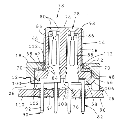
Intermediate flanges 22, aperture 42 extends through
diecast housing 12 from upper surface 18 to lower surface
20. Electrically conductive shroud 44 has a similar outer
profile to aperture 42 and is received therein in an
interference fit to assure electrical conductivity between
diecast hou~ng 12 and drawn shell 14. In a preferred
embodiment, the profile of shroud 44 is a subminiature D
which provides polarization of connector assembly 10
during mating with a complementary connector.
Shroud 44 of drawn shell 14 extends forwardly of a
substantially rectangular ~lange 46. Upon insertion of
drawn shell 14 into aperture 42 from the rear, that is
from the side of lower surface 20, flange 46 prevents
drawn shell 14 from passing through aperture 42 by
angaging surface 48 which extends around the periphery of
aperture 42. Seating ~lange 46 against surface 48 assures
1~91~2
--4--
that shroud 44 protrudes forward of upper surface 18 a
predetermined appropriate distance.
Also upon insertion of drawn shell 14 into aperture
42 the peripheral edge 50 of flange 46 engages
shell-to-shield grounding barbs on the interior endwalls
54 and sidewalls 56 of cavity 58. As best seen in Figures
2, 3 and 4, shell-to-shield grounding barbs 60 extend
inward from endwalls 54 into cavity 58; shell-to-shield
grounding barbs 62 extend inward from sidewalls 56 into
cavity 58. Grounding barbs 60 and 62 provide an
interference fit with the peripheral edge 50 that assures
electrical continuity between diecast housing 12 and drawn
shell 14.
Barbs 60, 62 extend from surface 48 alvng endwalls 54
and sidewalls 56 protruding into cavity 58 to interfere
with peripheral edge 50. Tapered surface 64 provides a
tapered lead in for flange 46 during insertion. In a
preferred embodiment barbs 60, 62 have the shape of a
triangular prism with apex 66 providing inter~erence with
peripheral edge 50. Alternatively, barbs 60, 62 could be
located on drawn shell 14 and engage diacast housing 12
such as along endwalls 54 or sidawalls 56.
~ arbs 60, 62 may be strateqically located to canter
drawn shell 14 in aperture 42 of diecast housing 12 such
as by two barbs on one wall and a centered barb on the
opposing wall, or by a pair of opposed barbs. Figure 2
shows a pair of opposed barbs 60 on endwalls 54 that
center drawn shell 14 laterally in aperture 42 and two
palrs of opposed barbs 62 on sidewalls 56 that each center
drawn shell 14 vertically in aperture 42.
An alternate embodiment diecast housing 12 and drawn
shell 1~ combination is shown in Figure 6 wherein tapered
barbs or protrusions 120 on drawn shell 14 paæs through
aperture 42 thenae snap outwardly to secure drawn shell 14
in di~cast housing 12. This alternate embodiment
~ 29~23Z
necessitates inserting drawn shell 14 into aperture 42
bafore inserting header insert 16 into drawn shell 14.
Upon inserting headsr insert into drawn shell 14, flange
member 122 flexes outwardly and housing 16 flexes inwardly
to permit header insert 16 to pass beyond barbs or
protrusions 124 which secures header insert 16 within
drawn shell 14. Barbs or protrusions 120, 124 may be
stamped or formed in drawn shell 14 during or after the
drawing process. Barbs 120 also assist in establishing
electrical continuity between diecast housing 12 and drawn
shell 14.
As drawn shell 14 is received in aperture 42, a burr
68 may form as peripheral edge 50 passes over apex 66 of
barbs 60, 62. To assure that flange 46 seats engaging
surface 48, a burr relief pocket 70 is formed in surface
48 around the periphery of aperture 42 at least in the
region of barbs 60, 62 to receive such a burr 68.
Header insert 16 is molded of thermoplastic and has
an insert portion 74, adapted to be received in shroud 44,
extending upwardly from integral peripheral flange 72.
Insert portion 72 has a similar outer profile to the
inside surface of an aperture in shroud 46 and is received
therein. Insert 16 has mating face 74, opposed rear face
76 and a plurality of contact receiving passages 78
extending from mating face 74 such as extending between
mating face 74 and rear face 76.
Contact receiving passages 78 typically have tapered
lead-in sur~aces 80 in mating face 74 to facilitate
mating. Contacts 82, which are inserted from rear face
76, are secured in contact receiving passages 78 such as
by barbs 84 that plow through the plastic forming
sidewalls 86 with the plastic flowing around barbs 84.
Contacts 82 have a mating portion 88 extending into
contact receiving passages 78 where sidewalls 86 may
provide an antioverstress ~unction, and a mounting portion
~J..2912~'32
90, typically solder posts 92, that extend beyond rear
face 76 for mounting such as in apertures 94 in printed
circuit board 96. Mounting portions so are then soldered
to traces on the upper and lower surfaces, 108 and 110
respectively, of printed circuit board 96. As best seen
in Figure 4, mounting portion 90 of every other contact 82
may be axially offset from the mating portion 88 of the
same contact 82 so as to provide a greater space bstween
adjacent apertures 94 in printed circuit board 960
Header insert 16 is inserted through cavity 58,
mating face 74 first, to seat within drawn shell 14 with
mating face 74 terminating proximate edge 98 of drawn
shell 14. Flange 72 of header insert 16 engages flange 46
of drawn shell 14 to assure that flange 46 engages diecast
housing 12 to provide electrical continuity between
diecast housing 12 and drawn shell 14 and secure drawn
shell 14 in position by clamping flange 46 between surface
48 of diecast housing 12 and flange 72 of header insert
16. Drawn shell 14 may include barb means to engage
insert 16 and to secure insert 16 in shell 14. The barb
means may take the form of a sheared, inwardly deflected
tab 112 as shown in section in Figure 14.
Barbs 60, 62 also provide a centering ~unction and
fit with header insert 16 to secure header insert 1~
within drawn shell 14 and cavity 58 as sidewall 100 of
flange 72 engage barbs 60, ~2. Header insert 16 is
further secured within diecast housing 12 by forming a
portion o~ housing 12 subsequent to inserting header
insert 16. The lower edge 102 of sidewall lO0 is moldad
at an angle and the lower sidewalls of diecast housing 12
is fabricated with a rib 104. Rib 104 is formed over edge
102 at one or more locatians forming diecast retention
feature 106 a~ shown on the left side of Figure 4 prior to
being formed and on the right side of Figure 4 subsequent
to being ~ormed~ ~n a pre~erred embodiment, lower edge
~ 2.g~23~
--7--
102 is molded at a 45 degree angle thus requiring rib 104
to be formed over only 45 degrees. Ribs 104 when formed
over provide a diecast retention feature 106 and are less
likely to fail than if formed through a large angle such
as 90 degrees.
Figure S shows an alternate embodiment connector
assembly 10 in which contacts 82 are formed with a 90
degree bend forming a connector in which the mating face
is at a right angle with respect to the mounting face.
~ lthough the connectors shown in the figures are for
"through board" mounting where mounting portion 90 of
contacts 82 pass through apertures 94 in printed circuit
board 96, the invention is not limited thereto. The
invention has application to surface mount technology
where apertures 94 are eliminated and mounting portions 90
are soldered to traces only on the side of printed circuit
board 96 on which connector assembly 10 is mounted.
Connector assembly 10 thus provides a combination of
a drawn shell which is proven for shielding with a diecast
housing that can be drilled and tapped thus minimizing
hardware and providing a durable latching surface.