Note: Descriptions are shown in the official language in which they were submitted.
'3~
The present invention relates to synthetic resin moldings
with a front and rear layer of different properties whereby
the front layer bears a printed surface capable of
backlighting (that is, capable of making the pictorial image
of lettering printed thereupon look bright if light is shone
from the rear of the product and when viewed from the front),
and to a method for the manufacture thereof.
It is common knowledge that backlighting products (that is,
products capable of making the pictorial image or letteriny
printed thereupon look bright if light is shone from the rear
of the product and when viewed from the front), are used in
various panels including automobile instrument panels and
front panels of audio products.
..... .
,~
~.,
~ 3 0~
These products are manufactured by imparting a printed
image on to a synthetic resin sheet and on to synthetic
resin moldings.
When a printed image is imparted on to a synthetic
resin sheet thereinafter referred to as sheet by way of
abbreviation?, it is possible to manuEacture a
multiplicity o~ 30 or 40 products simultaneously if a
sheet having a large sur~ace area is employed. I~,
however, a printed image is imparted on to a synthetic
resin molding (hereinafter referred to as molding by way
of abbreviation), it is possible to manufacture only a
very small number of a mere two or four simultaneously,
r~ thereby resultin~ in ~low productivity.
Even if a- of moldings were printed
simultaneously, it would, consequently~ be extremely
complicated and expensive to produce the holding jigs for
securing these moldings. And, further, even if it were
possible to produce high-accuracy holding jigs, the print
surfaces of the multiplicity of moldings would have
slightly different heights due to variations in the molded
products so that it would not be possible to achieve
high-quality products, and the operating result would be
most likely to give a low production yield.
3l.Z9~3(~8
Furthermore, the pxinting of moldings is a laborious
operation in view oE the extensive product handling
requir~ments so that it requires approximately dou~le the
number of operators than sheet printing does.
Moreover, if mulki-color printing is applied, the
moldings require repeated washing and handling to
thoroughly remove dust and dirt particles from the surface
so that some impact forces, minor though they may be
individually, will be applied to the molding. Under the
cumulative action of these frequently repeated impact
forces, however, the moldings will, in the course of time,
fracture, and protruding parts will break off.
For the printing of moldings it is essential that the
print surface should be flat. Yet, even if the molding
itself ~e flat, the holding jig tends to result in minor
incurvation and sloping of the surEace, thereby causing a
reduction in product quality and thus a drop in the
production yield.
Further, moldings are not always flat and will
occasionally be found to have convexities or concavities
on one or many of their sur~aces.
Furthermore, certain paxts may have convexities and
concavities on their surfaces.
3 -
9~3[)8
This renders the surface incapable of being printed,
except by the special printing technique known as pad
printing.
While printing by the pad printing method may produce
surfaces that appear perfect on cursory inspection, it
cannot meet the essential objective, since, with the use
oE backlighting, a process deemed necessary a]so for
molding such as automobile instrument panels and audio
products, and entailing that the printed pattern and
lettering should stand out clearly against the light shone
from the rear, the printed pattern and lettering that
should stand out clearly will appear to be riddled with
pinholes while the other ~normally black backgxound) parts
are suffused with light resulting in a pattern similar to
that oE a star-speckled sky at night.
Apart from those printing techniques involving the
direct application of print on to the molding, the
following methods are available for providing a print
surface to the molding.
One such method is known as the Simultranser System
(in-mold technique). This is a fully integrated molding
and printing system in which a transfer image foil is
positioned inside the injection molding die and the image
~ _
3C~8
is transferred onto the molding in the molding process, so
that the molding process and the transfer image application
process are accomplished in a single operation.
The problem associated with this process, however, lies in
the fact that since only the ink film layer printed on the
film is transferred on to the molding during the molding
process, the weld lines and gate marks generated on the
molding cannot be concealed so that the product's appearance
suffers.
Another such method is known as the heat transfer system, a
process in which a printed area (pattern), that is, a pattern
printed on a film, is heat-transferred on to a molding by
means of a hot stamping device.
The purpose of the present invention is therefore to provide
a method for the manufacture, at high quality and high
productivity, of moldings imparted with a printed area and
capable of backlighting.
The inventors of the present invention have, as a result of
the most dedicated and advanced research designed to overcome
the above problems, found out and
~. .,
-- 5 --
~l 29~30~3
discovered that it is possible to manufacture, at high
quality and high productivity, moldings possessing a front
and rear surface endowed with layers of different
properties and capable of backlighting, by printing a
synthetic resin sheet first by means of the screen
printing process, by then procesging this in a manner so
that the synthetic resin sheet thus printed can be charged
into the synthetic resin molding diel and by finally
injection-molding the molten resin after charging said
synthetic resin sheet therein and closing the die.
Thus, the present invention provides moldings
possessing a front or rear layer of dif~erent properties
and capable of backlighting, and a method for the
manufacture thereof by proceeding so that after printing,
by means of the screen printing method, in such a manner
that the thickness of the ink layer, applied as a simple
layer on a O.lmm - 2.0mm thick synthetic resin sheet, will
be 4~ or more (preerably 5~ or more), or that the
thickness of the ink film layer, applied in two or more
layers, will be 8~ or more (preferably 10~ or more), or,
alternatively, that the thickness of the ink film applied
as a simple layer will be 4~ or more (preferably 5y or
more) and the thickness of the ink layer applied in two or
- 6 -
~.29~301!3
more l.ayers wi.ll be ~ or mo:re tpreferably 10~ or- more), and
aEter processing in a form so that the synthetic resin sheet
thus printed can be charged inside -the mold:ing die, the die
is charged so that said synthetic resin sheet is adjacent to
the inner surface of the die, whereupon the molten resin for
the forming of the molding is in-jection-molded after said die
has been closed.
The inven-tion will now be described in more detail, by way of
example only, w.1th reference to the accompanying drawings in
which:
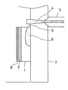
Fig. 1 is a partial cross-sec-tional view desiyned to
illustrate an embodiment of the present invention.
The synthe-tic resin sheet used in accordance with the present
invention is required to have a thickness from and including
1~ 0.1 mm up to and including 2.0 mm.
If it has a thickness of less than 0.1 mm, its mechanical
stren~th is not adequate when charged into the die and it may
separate from the die surface due to the structure of the
die.
Further, it will partially melt under the in~luence of the
hiyh temperature of the molten resin in the die so
9~3(~
that it will not be able to retain its shape.
Conversely, if the sheet has a thickness greater than
2.0mm it will not present problems when charged into the
die but will be a limiting factor when processing it to
such a shape that it can be charged into the die after it
has been printed, a problem that may arise when using a
punch die.
Since the processing operation has been performed by
cutting with a circular saw, for example, productivity
will have been substantially reduced so that this
operation is not feasible as an industrial production
process.
Moreover, when the die surface is curved, the sheet, if
thicker than 2.Omm, will not orient itself along the die
surface even when the molten resin is injection-molded, so
that the desired moldings cannot be obtained.
A major feature of the present invention is that it
permits printing on the curved surface areas of moldings
with curved surfaces. Yet, if a sheet of more than 2mm
thickness is used, the intentions of this invention will
be deviated from.
If the above synthetic resin sheet is printed by means
of a screen printing process, the thickness of the ink
-- 8 --
::
.
3~8
film layer applied as a single layer must be 4,u or more.
This thickness is the thickness after the ink has been
allowed to dry after printing.
The screen printing technique is ideally suited for
increasing the thickness of the ink film.
Other printing methods produce only a thin ink film Oe
l,u thickness or less at one pass.
If the ink ~ilm has a thickness of less than 4u, the
result will be the emergence of pinholes so that the
backlighting capability cannot be achieved.
If the printed section is black and forms the
background (that is, if there are no patterns and/or
lettering), it will be necessary to superimpose two print
layers so as to obtain an ink film thickness of 8~u or
more.
This is required because background sections tend to
give rise to pinholes more easily than printed patterns
and lettering do only in the large surface areas, thereby
leading to light effusion due to backlighting.
To charge a synthetic resin sheet printed in the manner
described above, it is processed to the shape of the die
aperture.
If the sheet is thin, it may be cut with scissors or
g _
~l.29~0~3
shears, and if it is thick, it may be cut with a circular
saw/ although this does not raise productivity.
It is therefore necessary to cut the sheet to the
required shape in a punching operation by preparing a
punch die and mounting it on -to a press for punching.
If the molding has perforations, the punch die should
be prepared so that perforations of khe same dimensions
and shape are obtained.
The punching dimensions for the printed sheet will
differ according as to the requirements specified for the
moldings.
If the printed sheet is stuck around the molding to
cover it as far as the side surfaces, the sheet should be
punched out to a size that exceeds the size of the
aperture of the molding die, and this only by the required
dimensions, and if it is an angular-shaped molding, the
four corners should be cut off.
After this, the parts around the sides are folded over
to impart a certain box-shape configuration.
If the molding surface and the printed sheet surface
have the same dimensions, the printed sheet may be punched
out to correspond to the die aperture.
In the two cases above, no problem will occur when the
-- 10 --
printed sheet is charged into the die.
The same also applies if the moldings have
perforations.
In this case, the perforations made in the printed
sheet should have the same dimensions as the molding die.
~f the molded resin surface is l:o be exposed at the
periphery oE the surfaces of the moldings, the printed
sheet should be made smaller only by the dlm~nsions to be
exposed.
In this case, minute apertures are made in the die and
these perforations are connected to a vacuum machine to
draw a vacuum so that the printed sheet inserted in the
die is firmly positioned and held on the molding die, with
the center o~ the die surface accurately aligned with the
center of the printed sheet.
The printed sheet is charged into the die in the manner
described above and the die is closed to inject the molten
resin for injection molding.
The path (gate) through which the molten resin is
intr~duced into the die should preferably be such that it
does not directly come into contact with the printed
sheet.
If the molten resin is brought in direct contact with
the sheet, the sheet may easily be destroyed under the
influence oE the high temperature and pressure of the
molten resin.
EX~MPLES
EXAMPLE l
Square-shaped white printed patterns o 105mm side length
were applied by the screen printing method on to a
polycarbonate sheet of 0.5mm thickness, 670mm height, and
450mm width, the number of squares totalling 24, being 6
lines x 4 stages at 3mm spacing in the horizontal.
The ink film thickness in these white print patterns
was 8,u. Printing was performed with black ink in such a
manner that ~peed markings from Okm/hr to 200km/hr and
lettering were applied, at a pitch of lkm/hr, as white
marks on the black background on a circular arc over an
angle range of 120 degrees, said circular arc of 45mm
radius being located within each of the squares and having
the same center as said squares~ that is, being concentric
therewith, said white markings and the white lettering
havlng a width o 0.5mm wldth and a length of 6mm3
Alternatively, such white blanked-out markings and the
- 12 -
~ ~ 9~ 3~ ~
white lettering of 2.Omm width and lOmm length,
respectively, wexe applied at a pitch of lOkm/hr..
All parts other than the punch markings and the punch
lettering were black, in other words, they formed the
background.
Printing with this black ink was performed twice, with
the second printing being superimposed upon the first
printing.
The film thickness after the superimposed double black
ink print application was a total of 15~.
The time required for printing amounted to 37 second~,
and the yield was approximately 96~ since one reject had
been encountered.
The printing was carried out by one printshop
operator.
This printed sheet was punched with a punching die,
along the white printed portion, to form a sheet oE 105mm
square to conform to the dimension of the 105mm square.
This sheet was charged into the cavity of the molding
die, made in such a manner that a molding of 3mm thickness
in the form of a square of 105mm side length was
obtained.
No particular devices and jigs were required for
- 13 -
charging the sheet into the die cavity, as the operation
was most easily performed manually taking approximately
one second.
The printed surface of the sheet was charged so that it
faced khe surface of the die cavity and though it did not
Porm a complete seal-contact with the die surface, this
did not impede the molding process in any way.
The die was closed and the molten acrylic resin was
injected for injection-molding under the normal conditions
generally applied in this process.
The gate had been prepared in such a manner that it was
parallel with the sheet.
The moldings thus obtained has a polycarbonate layer of
0.5mm thickness and had white speed markings from Okm/hr
to 200km/hr at an incremental pitch of lkm/hr each and
numbers in a s~uare of 105mm side length, with a thickness
of 3mm, while the surrounding background was black, and
when light was shone from the rear ~backlighting), the
markings and numbers did stand out clearly. Nor were there
any pinholes in the entire black background or any
effusion of light. (See drawing 1.)
EXAMPLE 2
- 14 -
~1.29~3~B
For the molding process, a die had been prepared in such a
manner that lOmm diameter perforations would appear in the
molding by imparting lOmm diameter projection onto the
center part of the die described in Example 1, or in such
a manner that the molding woulcl intersect the die sur~ace
in a circle o~ 48mm radius ~with the center oE the die
surface and the center of the circle aligned) by providing
spherical ~radius on the moving side of the die and by
producing spherical indentations o~ the same dimensions so
as to obtain a thickness of 3mm on the fixed ~immobile)
side of the die. Except or the use of this die, the
molding conditions were identical to those o Example 1.
The moldings thus obtained had white markings and
lettering left blank on the inner periphery o~ the
spherical recess, while the background was black and had
an attractive three-dimensional appearance.
When backlighting was applied to this, the markings and
lettering appeared to stand out very clearly, with no
pinholes and no light effusion being visible on the black
background.
EXAMPLE 3
The molding described in Example 2 was taken and a die was
- 15 -
308
prepared so that a frame of 3mm thickness and Smm height
was applied to its periphery.
Except for the fact that this was used and that a
polycarbonate net was employed as the molding resin to
obtain the molding, the molding process was performed
under the same conditions as khose given in Example 1.
The moldings thus obtained were 3mm in thickness and
105mm square, and the 0.5mm sur~ace layer had a
polycarbonate section, with Erame of 3mm thickness and 5mm
height applied to the peripheral part thereof, and having
white blanked-out markings and lettering on the inner
periphery of the spherical recess while the background had
an appealing black, three-dimensional appearance.
When backIighting was applied to this, the markings and
lettering appeared to stand out very clearly, with no
pinholes and conglomerations thereof and with no light
effusion being visible on the black background.
, ~
EXAMPLE 4
Except for the fact that on the white printing described
in Example 1, band of 8mm width were printed, with red
ink, so that the markings became red between 120km/hr and
200km/hr, the molding pxocess was performed by conducting
- 16 -
3~
a further printing operation, under the same conditions as
described in Example 1.
The moldings thus obtained had the same shape as those
of Example 1 and the lettering and the markings from
Okm/hr to 119km/hr were blanked out white while the speed
markings from 120km/hr to 200km/hr were blanked out red,
while the other parts were black.
The film thickness oE the white ink layer was 8,u while
the film thickness of the red ink layer was 6,u, whereas
the black ink layer which had been applied by
superimposing two layers had a total film thickness of
16~.
When backlighting was applied to this, the markings and
lettering appeared to stand out very clearly, with no
pinholes and no ligh~ effusion being visible on the black
background.
EXAMPLE 5
The thickness of the polycarbonate sheet used in Example 1
was made to be 2.0mm and printing was performed in the
same manner as in Example 1.
The film thickness of the white ink layer was 7~ and
the film thickness of the black ink layer was 17~.
- 17 -
~.Z~ 18
Except for the fact that after punching out the above
printed sheet to a 105mm square, the thickness was 5mm,
the same molding die as that descrlbed $n9Example 1 was
prepared and used, and the sheet ~ e~e~ in the cavity of
the die, the die closed and the molten resin
injection-molded.
The thickness of the resin part for molding was 3mm,
and the total thickness including the sheet layer was 5mm.
This led to a product having the same appearance as that
described in Example l.
There was no pinhole formation detectable under
backlighting.
EXAMPLE 6
A white print was applied, by the screen printing method,
~ to the entire surface area, except for a 5mm section on
; each periphery, of a polycarbonate sheet of 0~2mm
thickness, 580mm height, and 430mm width
~ The film thickness of this ink layer was 7~.
- Upon this, a total of 50 black print areas were applied
at a pitch of 40mm height and llOmm width each, so that
markings were obta.ined in the center from 0 to 100. In the
marking area corresponding to 60 a yellow print, and in
- 18 -
~l 2~30~3
the marking area corresponding to 80 a red print was
applied above the white print.
The respective film thicknesses were 9,u for the yellow
and 7,u for the red print areas.
Upon this, blanked out markings and lettering were
printed with black ink so that fine markings appreared at
a pitch oE 1 at a time from 0 to 100 and bold markings at
a pitch of 10. Moreover, on one side or one sideline rom
these blanked-out markings and lettering, 0.5mm large
blanked-out markings and lettering were superimposed in
black ink thereupon.
The total film thickness of the double black print was
20~.
The time required for printing totalled 75 seconds.
This is approximately 1/20th of the time required for
printing the moldings directly.
The molding die was prepared so that moldings with a
thickness dimension of 4rnm were obtained and had a short
side of 4cm and a long side of llcm, with the long side
describing a circular arc of 130mm radius.
The gate was provided parallel to the sheet at the end
of ther long side of the die.
The above printed sheet was punched out with a punohing
- 19 -
1 ~9~308
die at a pitch of 4cm height and llcm width so as to
produce a short sheet for molding.
The sheet thus obtained was inserted into the cavity of
the molding die ~recessed side of molding) in such a
manner that the non printed surface came in contact with
the die surface, when the dies was closed and the molten
acrylic resin injection-molded under the generally applied
conditions.
The moldings thus obtained had a short s.ide of 4cm and
a long side of llcm, with the long side having a simply
curved surface describing a circular arc of 130mm radius,
with the front surface having acrylic resin, and the rear
surface, polycarbonate resin fused thereon.
The acrylic resin of the front surface impart an
6l,p ;) Q ~f Q n C 4~ ,
apeeerane~ of depth to the markings and lettering, and the
'' '~,
application of backlighting showed no effusion of color.
The thicknesses of the ink films applied as single
layers in each of the above Examples were 8,u, 6~, 7,u and
9~, respectively, while the thicknesses of the ink films
applied as double layers were 15~, 16~, 17~ and 20~,
respectively. However, even when the former was 4~, and
the latter 8~, the result was the same in that no light
effusion was detectable.
- 2n -
~l.2~3~3Q8
COMPARISON 1
A molding oE 3mm thickness and 105mm square was obtained
by injection-molding using the die described in Example 1
and by using an acrylic resin.
Printing of the same nature as described in Example 1
was applied by preparing the setting jigs for the
screen-printing of these moldings.
White, black, and black printed patterns were applied
on a total of 24 moldings. The time required for this
printing operation amounted to 432 seconds, that is, seven
minutes and 12 seconds. This is roughly 12 times the time
required for printing in Example 1 which amounted to only
37 seconds.
Even after allowing for the time required for charging
the sheet into the molding die ~37 seconds + 24 seconds a
61 seconds), the printing takes roughly seven times the
time required in Example 1.
~ Even if the time re~uired for punching with a punching
; die, so as to charge the sheet into the molding die, is
countad and taken into consideration (61 seconds -~ 1
second/each x 24 = 85 seconds), it is clear that the
printing time is roughly five times that of Example 1.
- 21 -
~ ~<~C)8
The operation was performed by one operator, and five
rejects were encountered due to print misalignment and ink
smudging resulting from flatness deficiencies in the
moldings, so that the yield was 79.2%.
However, no light effusion and pinholes were observed
on backlighting.
COMPARISON 2
Moldings with lOmm diameter perforations in the center
were obtained, being 3mm thick and 105mm square and having
a shape such that the spherical projection of 250mm radius
intersect with the planar surface in a circle of 96mm
diameter, by using the molding die described in Example 2
and by using an acrylic resin for injection modling.
These moldings were then printed with patterns of the
same nature as those of Example 2 by using the PAD
printing method.
The white ink film thickness was l,u and the black film
applied in two layers had a tota1 thickness of 1.8,u. When
backlighting was applied, the light source was visible
through the transparent product which was therefore wholly
unfit for use.
- 22 -
~l.29~3(~
COMPARISON 3
The moldings were prepared with surface layers of
different properties by using a sheet printed by squeezing
the ink in such a manner as to obtain a white ink film
thicknes.s of 3~ and a superimposed double black ink film
thickness totalling 7~ as in Example 1. Upon backlighting,
these moldings showed seven to eight pinholes in the white
blanked-out parts whereas in the black background there
were two or three pinholes so that these products were not
suitable for use.
COMPARISON 4
When the 0.08mm sheet of Example 1 was used and charged
into the mo].ding die after printing and punching-out, it
was mechanically too weak to maintain its upright position
and bent over. Molding was per~fo.rmed in this condition,
. ., .~ _
when the sheet was found to cover only approximately two
thirds of the surface area of the molding while one third
of the molding resin was exposed.
COMPARISON 5
Printing was performed by using a sheet of 2.2mm thickness
instead of the sheet used in Example 5.
- 23 -
~'~9~3~)8
The punching die described in Example 5 was used for
punching, but the punching operation was not possible to
perform, and where punching was posslble it leEt bad nicks
and uneven edges so that the product was not fit for use
90 that the process was not pursued to the molding stage.
The present invention has the nature explained
hereinabove and has the superior advantages described
hereinbelow.
~1) Technical Simplicity
The present invention uses extremely simple technology in
that a printed synthetic resin sheet is charged into a
molding die and a molten resin injected into said molding
die to obtain moldings that are capable of backlighting.
A further technical characteristic is the facility with
which a printed surface with a thick ink film layer can be
securely maintained in the side of the molding.
The charging of the sheet into the molding die at the
time of molding is a simple operation.
(2) Molding with curved surfaces capable of backlighting
It is possible to impart, with great ease, a printed
surface with a thick film layer to the front or rear
~ 24 -
~ 3~8
surface of the molding with one or several curved surfaces
to achieve a backlighting capability.
(3) High Productivity
The process according to the present invention ha6 a
productivity several times that achievable with the direct
printing of moldings.
(4) Low ~eject Rate
The process according to the present invention is
characterized by a much lower reject rate than that
associated with the direct printing of moldings.
(5) Low Cost
The process according to the present invention has a low
cost eff~ct in that, by comparison with the direat
printing of moldings on a one-by-one basis, it permits the
simultaneous printing of a multiplicity of moldings.
(6) Attractive Appearance
The printed moldings obtained by the process according to
the present invention are of an attractive appearance and
do not present any of the weld lines and gate marks that
- 25 -
',
~Z9~0~3
tend to occur with such methods as the direct prinking of
moldings and the transfer-printing of an ink film from a
printed film onto a molding.
While there has been described what are at present
considered to be preferred embodiments of the invention,
it will be understood that various modifications may be
made thereto, and it is intended that the appended claims
cover all such modifications as fall within the true
spirit and scope of the invention.
- 26