Note: Descriptions are shown in the official language in which they were submitted.
a~
Field of the nvention
This invention relates to organic electro-
luminescent devices. More specifically, this inven-
tion relates to devices which emit light from anorganic layer positioned between anode and cathode
electrodes when a voltage is applied across the elec-
trodes.
~~8E~9n~ Of the Invention
While organic electroluminescent devices
have been known for about two decades, their perfor-
mance limitations have represented a barrier to many
desirable applications.
Gurnee et al U.S. Patent 3,172,862, issued
March 9, 1965, filed Sept. 29, 1960, disclosed an
organic electroluminescent device. (For brevity EL,
the common acronym for electroluminescent, is some-
times substituted.) The ~L device was formed of an
emitting layer positioned in conductive contact with
a transparent electrode and a metal electrode. The
emitting layer was formed of a con~ugated organic
host material, a con~ugated organic activating agent
having condensed benzene rings, and a f inely divided
conductlve material. Naphthalene, anthracene, phen-
anthrene, pyrene, benzopyrene, chrysene, picene, car-
bazole, fluorene, biphenyl, terphenyls, quaterphen-
yls, triphenylene oxide, dihalobiphenyl, trans-
stilbene, and 1,4-diphenylbutadiene were offered as
examples of organic host materials. Anthracene, tet-
racene, and pentacene were named as examples of acti-
vating agents, with anthracene being disclosed to
impart a green hue and pentacene to impart a red
hue. Chrome and brass were disclosed as examples oE
the metal electrode while the transparent electrode
was disclosed to be fl conductive glass. The phosphor
layer was disclosed to be "as thin as possible, about
~ / ~ .
0.0001 inch"- i.e., 2.54 micrometers. Elec~rolu~i-
nescence was reported at 800 volts and 2000 hertz.
Recognizing the disadvantage of employing
high voltages and frequencies Gurnee U.S. Patent
3,173,050 reported electroluminescence at llO volts
d.c. by employing in series with the emitt~ng layer
an impedance layer capable of accounting for 5 to 50
percent of the voltage drop across the electrodes.
Until relatively recently the art has
reported at best modest performance improvements over
Gurnee while resorting to increasingly challenging
device constructions, such as those requiring alkali
metal cathodes, inert atmospheres, relatively thick
monocrystalline anthracene phosphor elements, and/or
specialized device geometries. Mehl U.S. Patent
3,382,394, Mehl et al U.S. Patent 3,530,325, Roth
U.S. Patent 3,359,445, Williams et al U.S. Patent
3,621,321, Williams U.S. Patent 3,772,556, Kawabe et
al "Electroluminescence of Green Light Region ln
Doped Anthracene", JaPan Journal of ApPlled Physics,
Vol. 10, pp. 527-528, 1971, and Partridge U.S. Patent
3,995,299 ~re representative.
In 1969 Dresner, "Double In~ection Electro-
luminescence in Anthracene", RCA Review, Vol. 30, pp.
322-33~, independently corroborated the performance
levels of state of the art EL devices employing thick
anthracene phosphor elements, alkali metal cathodes,
and inert atmospheres to protect the alkali metal
from spontaneous oxidation. These EL devices were
more than 30 ~m in thickness and required operating
potentials of more than 300 volts. In attempting to
reduce phosphor layer thickness and thereby achieve
operation ~ith potential levels below 50 volts
Dresner attempted to coat ~nthracene powder between a
conductive glass anode and a gold, platinum or tellu-
rium grid cathode, but phosphor layer thicknesses of
5~
less than 10 ~m could not be successfully achieved
because of pinholes.
Dresner U.S. Patent 3,710,167 reported a
more promising EL device employing like Gurnee et al
and Gurnee a con~ugated organic compound, but as the
sole component of an emitting layer of less than 10
~m (preferably 1 to 5 ~m) in thickness. A tunnel
in~ection cathode consisting of aluminum or degener-
ate N silicon with a layer of the correspondi~g
aluminum or silicon oxide of less 10 Angstroms in
thickness was employed.
The most recent discoveries in the art of
organic EL device construction have resulted from EL
device constructions with two extremely thin leyers
(< 1.0 ~m in combined thickness) separating the
anode and cathode, one specifically chosen to trans-
port holes and the other specifically chosen to
transport electrons and acting as the organic lumi-
nescent zone of the device. This has allowed applied
voltages to be reduced for the first time into ranges
approaching compatibility with integrated circuit
drivers, such as field effect transistors. At the
same time light outputs at these low driving voltages
have been sufficient to permit observation under com-
mon ambient lighting conditions.
For example, Tang U.S. Patent 4,356,429 dis-
closes in Example 1 an EL device formed of a conduc-
tive glass transparent anode, a 1000 Angstroms hole
transporting layer of copper phthalocyanine, a 1000
Angstroms electron transporting layer o$ tetraphenyl-
butadiene in poly(styrene) also acting as the lumi-
nescent zone of the device, and a silver cathode.
The EL device emitted blue llght when blased at 20
volts at an average current denslty in the 30 to 40
mA/cm . The brightness of the device wes 5 cd/m .
Tang teaches useful cathodes to be those formed from
5~
common metals with R low work function, such ~9
indium, sllver, tin, and aluminum.
A further improvement in organic layer EL
devices is taught by Van Slyke et al U.S. Patent
4,539,507. Referring to Ex~mple 1, onto a transpar-
ent conductive glass anode were vacuum vapor depos-
ited successive 750 Angstrom hole transporting 1,1-
bis(4-di-P-tolylaminophenyl)cyclohexane and electron
transporting 4,4'-bis(5,7-di-t-pentyl-2-benzoxazo-
lyl)stilbene layers, the latter also providing theluminescent zone of the device. Indium was employed
as the cathode. The EL device emitted blue-green
light (5~0 nm peak). The maximum brightness achieved
340 cd/m2 at a current density of about 140 mA/cm2
when the applied voltage was 22 volts. The maximum
power conversion efficiency was about 1.4 X 10
watt/watt, and the maximum EL quantum efficiency was
about 1.2 X 10 photon/electron when driven at 20
volts. Silver, tin, lead, magnesium, manganese, and
aluminum are specifically mentioned for cathode con-
struction.
SummarY of the Invention
Although recent performance improvements in
organic EL devices have suggested a potential for
widespread u.~e, most practical applications require
limited voltage input or light output variance over
an extended period of time. The stability of the
device cathode has been a source of concern. Cathode
degradation results in obtaining progressively lower
current densities when a constant voltflge is
applied. Lower current densities in turn result in
lower levels of light output. With a constant
applied voltage practical EL device use terminates
when light emission levels drop below acceptable lev-
els -e.g., readily visually detectable emission lev-
els in ambient lighting. If the applied voltage is
progressively increased to hold light emission levels
constant, the field across the EL device i5 corre-
spondingly increased. Eventually a voltage level is
required that cannot be conv2niently supplied by the
EL device driving circuitry or which produces a field
gradient (volts/cm) exceeding the dielectric break-
down strength of the layers separating the elec-
trodes, resulting in a catastrophic failure of the ~L
device.
In choosing a cathode material it has been
recognized that the lowest work function metals most
readily release electrons for injection into the
electron transporting layer providing the organic
luminescent zone of the device. The lowest work
function metals are alkali metals. Their instability
in air renders alkali metals difficult to use in EL
device manufacture and unattractive for use in simple
device constructions requiring practical shelf and
operating lifetimes.
With alkali metals being re~ected, the art
has chosen to employ other low work function metals,
such as magnesium, or to forego the electron in~ec-
tion advantages of lower work function metals in
favor of greater cathode stability provided by some-
what higher work function metals, such as silver.
Another difficulty that has arisen in the
construction of organic EL devices is that it has not
been possible prior to this invention to achieve
efficient light emission through a cathode formed of
a low work function metal. Using a low work function
metal such as magnesium as an example, attempt~ to
form the metaL layer thin enough to permit efficient
light transmission has resulted in unacceptably high
sheet resistance. On the other hand, when the cath-
ode metal is coated thick enough to be acceptably
conductive, less than half the light received is
transmitted.
In one aspect this invention i5 directed. to
an electroluminescent device comprising in ~equence,
an anode, an organic hole transporting zone, an
organic electron transporting zone, and a cathode,
characterized in that the cathode is comprised oE a
layer consisting essentially of a plurality of metals
other than alkali metals, at least one of the metals
having a work function of less than 4 eV.
It has been discovered quite unexpectedly
that the foregoing combination of a low work function
metal and at least one other metal in the cathode of
an organic EL device results in improving the sta-
bility of the cathode and therefore the stabiliky of
the device as a whole. It has been observed that the
initial performance advantages of low work function
metals other than alkali metals as cathode materials
are only slightly diminished when combined with more
stable, higher work function metals while marked
extensions of EL device lifetimes are realized with
even small amounts of a second metal being present.
Further, the advantages in extended lifetimes can be
realized even when the cathode metals are each low
work function metals other than alkali metals. Addi-
tionally, the use of combinations of metals in form-
ing the cathodes of the organic EL devices of this
invention has resulted in unexpected advantages in
fabrication, such as improved acceptance by the elec-
tron transporting organic layer during vacuum vapor
deposition of the cathode.
Another unexpected advantage realized with
the cathode metal combinations of this invention i5
that low work function metals can be employed to pre-
pare cathodes which are light transmissive and at the
same time exhibit low levels of sheet resistance.
Thus, the optlon is afforded of organic EL device
constructions in which the anode need not perform the
5~ .
function of light transmission, thereby affording new
use opportunities ~or organic EL devices.
Brief DescriPtion of the Drawin2s
These and other advantages of the present
invention can be better appreciated by reference to
the following detailed descrlption consldered in con-
~unction with the drawings, in which
Figures 1, 2, and 3 are schematic diagrams
of EL devices;
~O Figures 4 and 5 are micrographs of conven-
tional and inventive cathodes, respectively.
The drawings are necessarily of a schematic
nature, since the thicknesses of the individual lay-
ers are too thin and thickness differences of the
various device elements too great to permit depiction
to scale or to permit proportionate scaling.
DescriPtion of Preferred Embodiments
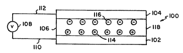
An electroluminescent or EL device 100
according to the invention is schematically illus-
~O trated in Figure 1. Anode 102 is separated fromcathode 104 by an organic luminescent medium 106.
The anode and the cathode are connected to an exter-
nal power source 108 by conductors 110 and 112,
respectively. The power source can be a continuous
direct current or alternating current voltage source
or an intermittent current voltage source. Any con-
venient conventional power source, including any
desired switching circuitry, can be employed which is
capable of positively biasing the anode with respect
to the cathode. Either the anode or cathode can be
at ground potential.
~ he EL device can be viewed as a diode which
is forward biased when the anode is at ~ higher
potential than the cathode. Under these conditions
the anode in~ects holes (positive charge carriers),
schematically shown at 114, into the luminescent
medium while the cathode in~ects electrons, schemati-
cally shown at 116, into the luminescent medium. Theportion of the luminescent medium ad~Acent the ~node
thus forms a hole transporting 20ne while the portion
of the luminescent medium adjacent the cathode forms
an electron transporting zone. The in~ected holes
and electrons each migrate toward the oppositely
charged electrode. This results in hole-electron
recombination within the organic luminescent medium.
When a migrating electron drops from its conduction
potential to a valence band in filling a hole, energy
is released as light. Hence the organic luminescent
medium forms between the electrodes a luminescence
zone receiving mobile charge carriers from each elec-
trode. Depending upon the choice of alternative con-
lS structions, the released light can be emitted from
the luminescent material through one or more of edges
118 separating the electrodes, through the anode,
through the cathode, or through any combination of
the foregoing.
Reverse biasing of the electrodes disrupts
charge injection, depletes the luminescent medium of
mobile charge carriers, and terminates light emis-
~ion. The most common mode of operating organic EL
devices is to employ a forward biAsing d.c. power
source and to rely on external current interruption
or modulation to regulate light emission.
In the organic EL devices of the invention
it is possible to maintain a current density compati-
ble with ef~icient light emission while employing a
relatively low voltage across the electrodes by lim-
iting the total thickneqs of the organic luminescent
medium to less than 1 ~m (10,000 Angstroms). At a
thickness of less than 1 ~m an applied voltage of 20
volts results in a field potential of greater than
2 X 10 volts/cm, which is compatible with effi-
cient light emission. As more speciEically noted
below, an order of magnitude reduction ~to 0.1 ~m or
l000 Angstroms) in thickness of the organic lumines-
cent medium, allowing further reductions in Applied
voltage and/or increase in the field potential, ~re
well within device construction capabilities.
Since the organic luminescent medium is
quite thin, it is usually preferred to emit light
through one of the two electrodes. This is achieved
by forming the electrode as A translucent or trans-
parent coating, either on the organic luminescent
medium or on a separate translucent or transparent
support. The thickness of the coating is determined
by balancing light transmission (or extinction) and
electrical conductance (or resistance). A practical
balance in forming a light transmissive metallic
electrode is typically for the conductive coating to
be in the thickness range of from about 50 to 250
Angstroms. Where the electrode is not intended t~
transmit light, any greater thickness found conve-
nient in fabrication can also be employed.
Organic EL device 200 shown in Figure 2 is
illustrative of one preferred embodiment of the
invention. Because of the hi~torical development of
organic EL devices it is customary to employ a trans-
parent anode. This has been achieved by providing a
transparent insulative support 201 onto which is
deposited a conductive relatively high work function
metal or metal oxide transpArent layer to form anode
203. Since the portion of the organic luminescent
medium immediately ad~acent the anode acts as A hole
transporting zone, the organic luminescent medium i9
preferably formed by depositing on the anode a layer
205 of an organic material chosen for its hole trans-
porting efficiency. In the orientation of the device
200 shown, the portion of the organic luminescent
medium adjacent it-~ upper surface constitutes an
electron transporting zone and is formed of a layer
207 of an organic material chosen for its electron
~L2~
-10-
transporting efficiency. With preferred choices of
materials, described below, forming the layers 205
and 207, the latter also forms the zone ln which
luminescence occurs. The cathode Z09 is conveniently
formed by deposition on the upper layer of the
organic luminescent medium.
Organic EL device 300 shown in Figure 3 is
illustrative of another preferred embodiment of the
invention. Contrary to the historical pattern of
organic EL device development, light emission from
the device 300 is through the light transmissive
(e.g., transparent or substantially transparent)
cathode 309. While the anode of the device 300 can
be formed identically as the device 200, thereby per-
lS mitting light emission through both anode and cath-
ode, in the preferred form shown the device 300
employs an opaque charge conducting element to form
the anode 301, such as a relatively high work func-
tion metallic substrate. The hole and electron
transporting layers 305 and 307 can be identical to
the corresponding layers 205 and 207 of the device
200 and require no further description. The signifi-
cant difference between devices 200 and 300 is that
the latter employs a thin, light transmissive (e.g.,
transparent or substantially transparent) cathode in
place of the opaque cathode customarlly included in
organic EL devices.
Viewing organic EL devices 200 and 300
together, it is apparent that the present invention
offers the option of mounting the devices on either a
positive or negative polarity opaque substrate.
Unexpected fabrication, performance, and
stability advantages have been reali~ad by forming
the cathode of a combination of a low work function
metal and at least one other metal. A low work func-
tion metal is herein defined as a metal having ~ work
function of less than 4 eV. Generally the lower the
~:9~
work function of the metal, the lower the voltage
required for electron in~ection into the organic
luminescent medium. However, alkali metals, the low-- ;
est work function metals, are too reactive to achieve
stable EL device performance with simple device con-
structions and construction procedures and are
excluded ~apart from impurity concentrations) from
the cathodes of this invention.
Available low work function metal choices
for the cathode (other alkali metals) are listed
below by periods of the Periodic Table of Elements
and categorized into 0.5 eV work function groups.
All work functions provided are taken Sze, PhYsics of
Semiconductor Devices, Wiley, N.Y., 1969, p. 366.
Work Function
Period Element By eV Group
2 Beryllium 3.5 - 4.0
3 Magnesium 3.5 - 4.0
4 Calcium 2.5 - 3.0
Sc~ndium 3.0 - 3.5
Titanium 3.5 - 4.0
Manganese 3.5 - 4.0
Gallium 3.5 - 4.0
Strontium 2.0 - 2.5
Yttrium 3.0 - 3.5
Indium 3.5 - 4.0
6 Barium ~2.5
Lanthanum 3.0 - 3.5
Cerium 2.5 - 3.0
. Praseodymium 2.5 - 3.0
Neodymium 3.0 - 3.5
Promethium 3.0 3.5
Samarium 3.0 - 3.5
Europium 2.5 - 3.0
Gadolinium 3.0 - 3.5
Terbium 3.0 - 3.5
Dysprosium 3.0 - 3.5
-12-
Holmium 3.0 - 3.5
Erbium 3.0 - 3.5
Thulium 3.0 - 3.5
Ytterbium2.5 - 3.0
Lutetium3.0 - 3.5
~afnium ~3.5
7 Radium 3.0 - 3.5
Actinium2.5 - 3.0
Thorium 3.0 - 3.5
Uranium 3.0 - 3.5
From the foregoing listing it is apparent
that the available low work function metals for the
most part belong to the Group IIa or alkaline earth
group of metals, the Group III group of metals
(including the rare earth metals - i.e. yttrium and
the lanthanides, but excluding boron and aluminum),
and the actinide groups of metals. The alkaline
earth metals, owing to their ready availability, low
cost, ease of handling, and minimal adverse environ-
mental impact potential, constitute a preferred classof low work function metals for use in the cathodes
of EL devices of this invention. Magnesium and cal~
cium are particularly preferred. Though signifi-
cantly more expensive, the lncluded Group III metals,
particularly the rare earth metals, possess similar
advantages and ~re specifically contemplated as pre-
ferred low work function metals. The low work func-
tion metals exhibiting work functions in the range of
from 3.0 to 4.0 eV are generally more stable than
metals exhibiting lower work functions and are there-
fore generally preferred.
A second metal included in the construction
of the cathode has a~ one primary purpose to increase
the stability (both storage and operatlonal) of the
cathode. It can be chosen from among any metal other
than an alkali metal. The second metal can itself be
a low work function metal ~nd thus be chosen from the
~L2~ 5~
-13-
metals listed above having ~ work function of less
than 4 eV, with the same preferences above di~cu~ed
being fully applicable. To the extent that the ~ec-
ond metal exhibits a low work function it can, of
course, supplement the first metal in facilitating
electron in~ection.
Alternatively, the second metal can be cho-
sen from any of the various metals having a work
function greater than 4 eV, which includes the ele-
ments more resistant to oxidation and therefore morecommonly fabricated as metallic elements. To the
extent the second metal remalns invariant in the
organic EL device as fabricated, it contributes to
the stability of the device.
Available higher work function (4 eV or
8reater) metal choices for the cathode are listed
below by periods of the Periodic Table of Elements
and categorized into 0.5 eV work function groups.
Work Function
Period ElementBY eV Group
2 Boron 4.5
Carbon4.5 - 5.0
3 Aluminum4.0 - 4.5
4 Vanadium4~0 - 4.5
Chromium4.5 - 5.0
Iron 4.0 - 4.5
Cobalt4.0 -- 4.5
Nickel ~4.5
Copper4.0 - 4.5
Zinc 4.0 - 4.5
Germanium4.5 - 5.0
Ar~enic5.0 - 5.5
Selenium4.5 - 5.0
Molybdenum 4~0 - 4.5
Technetium 4.0 - 4.5
Ruthenium4.5 - 5.0
Rhodium4.5 - 5.0
-14-
Palladium4.5 -- 5.0
Silver 4.0 - 4.5
Cadmium 4.0 - 4.5
Tin ~.0 - ~.5
Antimony4.0 - 4.5
Tellurium4.5 - 5.0
6 Tantalum4.0 - 4.5
Tungsten ~4.5
Rhenium ~5.0
Osmium 4.5 - 5.0
Iridium 5.5 - 6.0
Platinum5.5 - 6.0
Gold 4.5 - 5.0
Mercury ~4.5
Lead ~4.0
Bismuth 4.0 - 4.5
Polonium4.5 - 5.0
From the foregoing listing of available met-
als having a work function of 4 eV or greater attrac-
tive higher work function metals for the most partare accounted for by aluminum, the Group Ib metals
(copper, silver, and 801d), the metals in Groups IV,
V, and VI, and the Group VIII transition metals, par-
ticularly the noble metals from this group. Alumi-
num, copper, silver, gold, tin, lead, bismuth, tellu-
rium, and antimony are particularly preferred higher
work function second met~ls for incorporstion in the
cathode.
There are several reasons for not restrict-
ing the choice of the second metal based on eitherits worX function or oxidative stability. The ~econd
metal is only a minor component of the cathode. One
of its primary functions is to stabilize the first,
low work function metal, and, ~urprisingly, it accom-
plishes this ob~ective independent of its own workfunction and susceptibility to oxidation.
5S~
-15-
A second valuable function which the ~econd
met~l performs is to reduce the sheet resistance of
the ca~hode as a function of the thickness of the
cathode. Since acceptably low sheet resistance lev-
els (less than 100 ohms per square) can be reRlizedat low cathode thicknesses (less than 250 ~ngstroms),
cathodes can be formed which exhibit high levels of
light transmission. This permits highly stable,
thin, transparent cathodes of acceptably low resis-
tance levels and high electron injecting eEficienciesto be achieved for the first time. This in turn per-
mits (but does not require) the organic EL devices of
this invention to be constructed with light transmis-
sive cathodes and frees the organic EL devices of any
necessity of havlng a light transmissive anode to
achieve light emission through an electrode area.
A third valuable function which the second
metal has been observed to perform is to facilitate
vacuum vapor deposition of a ~irst metal onto the
organic luminescent medium of the EL device. In
vapor deposition less metal is deposited on the walls
of the vacuum chamber and more metal is deposited on
the organic luminescent medium when a ~econd metal is
also depo~ited. The efficacy of the second metal in
stabilizing organic EL device, reducing the sheet
resistance of thin cathodes, and in improving accep-
tance of the first metal by the organic luminescence
medium is demonstrated by the examples below.
Only a very small proportion of a second
metal need be present to achieve these advantages.
Only about 0.1 percent of the total metal atoms of
the cathode need be accounted for by the second metal
to achieve a substAntial improvement. Where the sec-
ond metal is itself a low work function metal, both
the first and second metals are low work function
metals, and it i~ immaterial which is regarded as the
first metal and which is regarded as the second
~l2~
-16-
metal. For example, the cathode composition can
range from about 0.1 percent of the metal fltoms of
the cathode being accounted for by one low work func-
tion metal to about 0.1 percent of ~he total metal
atoms being accounted for by a second low work func-
tion metal. Prefer~bly one of the two metals
accounts for at least l percent and optimally at
least 2 percent of the total metal fltoms present.
When the second metal is a relatively hi~her
(at least 4.0 eV) work function metal, the low work
function metal preferably accounts for greater than
50 percent of the total metal atoms of the cathode.
This is to avoid reduction in electron in;ection
efficiency by the cathode, but it is also predicated
on the observation that the benefits of adding a sec-
ond metal are essentially realized when the second
metal accounts for less than 20 percent of the total
met~l atoms of the cathode.
Although the foregoing discussion has been
in terms of a binary combination of metals forming
the cathode, it is, of course, appreciated that com-
binations of three, four, or even higher numbers of
metals are possible and can be employed, if desired.
The proportions of the first metal noted a~ove can be
accounted for by any convenient combination of low
work function metals and the proportions of the sec-
ond metal can be accounted for any combination of
hi8h and/or low work function metals.
While the second metal or metals can be
relied upon to enhance electrical conductivity, their
minor proportion of the total cathode metal renders
it unnecessary that these metals be present in fln
electrically conducting form. The second metal or
metals can be present as compounds (e.g., lead, tin,
or antimony telluride) or in an oxidized form, such
as in the form of one or more metal oxides or sfllts.
Since the flrst, low work function metal or metals
~15S~
account for the major proportion of the cathode metal
content and are relied upon for eleckron conduction,
khey are preferably employed in their elemental form,
although some oxidation may occur on aging.
The manner in which the presence of a second
metal physically intervenss to enhance cathode sta-
bility and light transmission enhancement whlle
reducing sheet resistance can be appreciated by com-
paring Figures 4 and 5. Figure C~ is a micrograph,
enlarged to the scale indicated, of A vacuum vapor
deposited conventional, prior art cathode consisting
of magnesium. The thickness of the magnesium coating
is 2000 Angstroms. The non-uniformity of the coat-
ing, detracting both from its electrical conductivity
and its ability to transmit light, is readily appar-
ent. Because of its non-uniformity the coating is
also more readily penetrable and therefore more sus-
ceptible to oxidative degradation.
In direct contrast, the cathode of Figure 5
illustrating the invention, also 2000 Angstroms in
thickness, is smooth and featureless. This cathode
is formed by the vacuum vapor deposition of magnesium
and silver, with the magnesium and silver being pres-
ent in an atomic ratio of 10:1. That is, the silver
atoms are pre~ent ln a concentration of 9 percent of
total metal atoms present. The imperceptibly low
granularity of the invention cathode is indicative of
8 higher and more uniform coverage of the deposition
substrate. Identical sub~trates were employed in
forming the Figures 4 and 5 coatings.
In depositing the first metal alone onto a
substrate or onto the organic luminescent medium,
whether from solution or, preferably, from the vapor
phase, initial, -~patially separated deposits of the
first metal form nuclei for subsequent deposition.
Subsequent deposition leads to the growth o~ these
nuclei into microcrystals. The result is an uneven
-18-
and random distribution of microcrystals, leading to
A non-uniform cathode. By prQsenting a second metal
during at least one of the nucleation and growth
stages and, preferably, both, the high degree of -~ym-
metry which a single element affords is reduced.
Since no two substances form crystal cells of e~actly
the same ha~it and size, any second metal reduces the
degree of symmetry and at least to some extent acts
to retard microcrystal growth. Where the flrst and
second metals have distinctive crystal habits, spa-
tial symmetry is further reduced and microcrystal
growth is further retarded. Retarding microcrystal
growth favors the formation of additional nucleation
sites. In this way the number of deposition sites is
increased and a more uniform coating is achieved.
Depending upon the specific choice of met-
als, the second metal, where more compatible with the
substrate, can produce a disproportionate number of
the nucleation sites, with the first metal then
depositing at these nucleation sites. Such A mecha-
nism may, if fact, account for the observation that,
with a second metal present, the efficiency wlth
which the first metal is accepted by a substrate is
significantly enhanced. It has been observed, for
example, that less deposition oE the first metal
occurs on vacuum chamber walls when a second metal is
being co-deposited.
The first and second metals of the cathode
are intimately intermingled, being co-deposited.
That is, the deposition of neither the first nor sec-
ond metals is completed before at least a portion of
the remainin8 metal is deposited. Simultaneous depo-
sition of the first and second metals is generally
preferred. Alternatively, successive incremental
depositions of the first and second metals csn be
undertaken, which at their limit may approximate con-
current deposition.
~;~9~
-19-
While not required, the cathode, once formed
can be given post treatments. For example, the cath--
ode may be heated wi~hin the stability limits of the
substrate in a reducing atmosphere. Other action on
the cathode can be undertaken as a conventionally
attendant feature of lead bondlng or device encapsu-
lation.
The organic luminescent medium of the EL
devices of this invention preferably contains at
least two separate organic layers, at least one layer
forming a zone for transporting electrons injected
from the cathode and at least one layer forming a
zone for transporting holes injected from the anode.
The latter zone is in turn preferably formed of at
least two layers, one, located in contact with the
anode, providing a hole injecting zone and the
remaining layer, interposed between the layer forming
the hole in;ecting zone and the layer providing the
electron transporting zone, providing a hole trans-
porting zone. While the description which follows isdirected to the preferred embodiments of organic EL
devices according to this invention which employ at
least three separate organic layers, it is appreci-
ated that either the layer forming the hole in~ecting
zone or the layer forming the hole transporting zone
can be omitted and the remaining layer will perform
both functions. Higher initial and sustained perfor-
mance level~ of the organic EL devices of this inven-
tion are realized when the separate hole in~ecting
and hole transporting layers described below are
employed in combination.
A layer containing a porphyrinic compound
forms the hole in~ecting zone of the organic EL
device. A porphyrinic compound is any compound,
natural or synthetic, which is derived from or
includes the porphyrin structure. Any of the por-
phyrinic compounds disclosed by Adler U.S. Patent
12~S~
-20-
3,935,031 or Tang U.S. Patent 4,356,429, can be
employed.
Preferred porphyrinic compounds ar~ those of
structural formula (I):
5 (I) Tl T2
\.=./
T~ T
i~ M~
T2/ \ I ~./ \T2
~Q,.~ \.,~Q/
~ \ 2
wherein
Q is -N= or -C(R)=;
M is a metal, metal oxide, or metal halide;
R is hydrogen, alkyl, aralkyl, aryl, or alkaryl,
and
T and T represent hydrogen or together com-
plete a unsaturated 6 membered ring, which can
include substituents, such as alkyl or halogen. Pre-
ferred alkyl moieties contain from about 1 to 6 car-
bon atoms while phenyl constitutes a preferred aryl
moiety.
In an alternative preferred form the por-
phyrinic compounds differ from those of structural
formula (I) by substitution of two hydrogen for the
metal atom, as indicated by formula (II):
3S
~9~L5~
(II) ~ T2
T~ T2
T2/ \ ~ ~ ~ ./ ~ 2
~,./N\.~Q! .
~ \ 2
Highly preferred examples of useful porphyr-
inic compounds arP metal free phthalocyanines and
metal containing phthalocyanines. While the porphyr-
inic compounds in general and the phthalocyanines in
particular can contain any metal, the metal prefera-
bly has a positive valence of two or higher. Exem-
plary preferred metals are cobalt, magnesium, zinc,
palladium, nickel, and, particularly, copper, lead,
and platinum.
Illustrative of u~eful porphyrinic compounds
are the follow1ng:
PC-l Porphine
PC-2 1,10,15,20-Tetraphenyl-21H,23H -porphine
copper (II)
PC-3 1,10,15,20-Tetraphenyl-21H,23H -porphine
zinc (II)
PC-4 5,10,15,20-Tetrakis(penta$1uorophenyl)-
21H,23H-porphine
PC-5 Silicon phthalocyanine oxide
PC-6 Aluminum phthalocyanine chloride
PC-7 Phthalocyanine (metal free)
PC 8 Dillthium phthalocyanine
PC-9 Copper ~etramethylphthalocyanine
PC-10 Copper phthalocyanine
PC-ll Chromium phthalocyanine fluoride
PC-12 Zinc phthalocyanine
PC-13 Lead phthalocyanine
~9~s~ ~
-22-
PC-14 Titanium phthalocyanlne oxide
PC-15 Magnesium phthalocyanine
PC~16 Copper octamethylphthalocyanine
The hole transporting layer of the organic
EL device contains at least one hole transporting
aromatic tertiary Rmine, where the latter is under-
stood to be a compound containing at least one triva-
lent nitrogen atom that is bonded only to carbon
atoms, at least one of which is a member of an aro-
matic ring. In one form the aromatic tertiary aminecan be an arylamine, such as a monoarylamine, diaryl-
amine, triarylamine, or a polymeric arylamine. Exem-
plary monomeric triarylamines are illustrated by
Klupfel et al U.S. Patent 3,180,730. Other suitable
triarylamines substituted with vinyl or vinylene
radicals and/or containing at least one active hydro-
8en containing group are disclosed by Brantley et al
U.S. Patents 3,567,450 and 3,658,520.
A preferred class of aromatic tertiary
amines are those which include at least two aromatic
tertiary amine moieties. Such compounds include
those represented by structural formula (III):
(III) Q1 Q2
\G/
wherein
Q and Q are independently aromatic tertiary
amine moieties and
G is a linking group such an arylene, cycloalkyl-
ene, or alkylene group or a carbon to carbon bond.
A particularly preferred class of triaryl-
amines satisfying structural formula (III) and con-
taining two triarylamine moieties are those ~atisfy-
ing structural formula (IV):
~L~g~i5~
(IV) R
Rl- C - R3
l4
where
R and R each independently represents a
hydrogen atom, an eryl group or alkyl group.or
and R together represent the atoms completing a
cycloalXyl group and
R3 and R4 each independently represents an
aryl group which is in turn subs~ituted with a diaryl
substituted amino group, as indicated by structural
formula (V):
(V) 5
_ ~
\R6
wherein R5 and R6 are independently selected aryl
groups.
Another preferred class of aromatic tertiary
amines are tetraaryldiamines. Preferred tetraaryldi-
amines lnclude two diarylamino groups, such a~ indi-
cated by formula (V3, linked through an arylene
group. Preferred tetraaryldiamines include those
repre~ented by f ormula (VI).
25 (VI) R7 R8
Ar~ Aren N\R9
wherein
Are i an arylene group,
n is an inte8er of from l to 4, and
Ar, R , R8, and R are independently
~elected aryl groups.
The various alkyl, alkylene, aryl, and aryl--
ene moieties of the foregoing structural formulae
(III), (IV), (V), and (VI) can each in turn be sub-
stituted. Typical substituents including alkyl
i .
5~L
-2~-
groups, alkoxy groups, aryl groups, aryloxy groups,
and halogen such as fluoride, chloride, and ~romide.
The v~rious alkyl and alkylene moieties typically
contain from about l to 5 carbon atoms. The cycloal-
kyl moieties can contain from 3 to about lO c~rbonatoms, but typically contain five, six, or seven ring
carbon atoms--e.g., cyclopentyl, cyclohexyl, snd
cycloheptyl ring structures. The aryl and arylene
moieties are preferably phenyl and phenylene moieties.
While the entire hole transporting layer of
the organic electroluminesce medium can be formed of
a single aromatic tertiary amine, it is a further
recognition of this invention that increased sta
bility can be realized by employing a combination of
aromatic tertiary amines. Specifically, as demon-
strated in the examples below, it has been observed
that employing a triarylamine, such as a triarylamine
satisfying formula tIV), in combination with a tetr~-
aryldiamine, such as indicated by formula (VI), can
be advantageous. When a triarylamine is employed in
combination with a tetraaryldiamine, the latter is
positioned as a layer interposed between the triaryl-
amine and the electron in~ecting and transporting
layer.
Representative useful aromatic tertiary
amines are disclosed by Berwick et al U.S. Patent
4,175,960 and Van Slyke et al U.S. Patent 4,539,507.
Berwick et al in addition discloses as useful hole
transporting compounds N substituted carbazoles,
which can be viewed as rin8 brid8ed variants of the
diaryl and triarylamines disclosed above.
Illustrative of useful aromatic tertiary
amines are the following:
ATA~ l-Bis(4-di~-tolylaminophenyl)cyclo-
hexane
ATA-2 l,l-Bis(4-di-~-tolylaminophenyl)-4-
phenylcyclohexane
~2 9
-25-
ATA-3 4,4'-Bis(diphenylamino)quadriphenyl
ATA-4 Bis~4-dimethylamino-2-methylphenyl)-
phenylmeth~ne
ATA-5 N,N,N-Tri(~-tolyl)amine
ATA-6 4-(di ~-tolylamino)-4'-[4(di-p-tolyl-
amino)styryl]stilbene
ATA-7 N,N,N',N'-Tetra-~-tolyl-4,4'-diaminobi-
phenyl
ATA-8 N,N,N',N'-Tetraphenyl-4,4'-diaminobi-
phenyl
ATA-9 N-Phenylcarbazole
ATA-10 ~ Poly(N-vinylcarbazole)
Any conventional electron in;ecting and
transporting compound or compounds can be employed in
forming the layer of the organic luminescent medium
ad~acent the cathode. This layer c~n be formed by
historically taught luminescent materials, such as
anthracene, naphthalene, phenanthrene, pyrene, chrys-
ene, and perylene and other fused ring luminescent
materials containing up to about 8 fused rings as
illustrated by Gurnee et al U.S. Patent 3,172,862,
Gurnee U.S. Patent 3,173,050, Dresner, "Double In~ec-
tion Electroluminescence in Anthracene", RCA Review,
Vol. 30, pp. 322-334, 1969; and Dresner U.S. Patent
3,710,167, cited above. Although quch fused ring
luminescent materials do not lend themselves to fo~m-
ing thin (< 1 ~m) films and therefore do not lend
themselves to achieving the highest attainable EL
device performance levels, organic EL devices incor-
porating such lumlnescent materials when constructedaccording to the invention show improvements in per-
formance and stability over otherwise comparable
prior art EL devices.
Among electron transporting compounds useful
in forming thin films are the butadienes, such as
1,4-diphenylbutadiene and tetraphenylbutadiene; cou-
129~S5~
-26-
marins; and stilbenes, such as trans-stilbene, dis-
closed by Tang U.S. Patent 49356,429, cited above.
Still other thin film forming electron
transporting compounds which can be used to form the
layer ad~Acent the cathode are optical brighteners,
particularly those disclosed.by Van Slyke et al U.S.
Patent 4,539,507, cited above. Useful optical
brighteners include those satisfying structural for-
mulae (VII) and (VIII):
lo (VII) Rl f \ ~ ~ ~ N\ ~ or
2~ / \Z/ \ Z/ ~ ~ 4
(VIII) 3 R5
1 ~ /li\ 9 ~: i
wherein
R , R , R , and R are individually
hydrogen; saturated aliphatic of from 1 to 10 carbon
atoms, for example, propyl, t-butyl, heptyl, and the
like; aryl of from 6 to 10 carbon atoms, for example,
phenyl and naphthyl; or halo such as chloro, fluoro,
and the like; or R and R2 or R and R4 taken
together comprise the atoms necessAry to complete a
fused aromatic ring optionally bearing at least one
saturated aliphatic of from 1 to lO carbon Atoms,
such as methyl, ethyl, propyl and the like;
R is A sRturated aliphatic of from 1 to 20
carbon atoms, such as methyl, ethyl, n--eicosyl, and
the like; aryl of from 6 to 10 carbon Rtoms, for
example, phenyl and naphthyl; carboxyl; hydrogen;
cyano; or halo, for example, chloro, Eluoro and the
like; provided that in formula (VII) at least two of
R , R and R ~re saturated aliphatic of from 3
~9~
-~7-
to 10 carbon atoms, e.g., propyl, butyl, heptyl and
the like;
Z is -O-, NH-, or -S-; and
Y i~
R ~CH H~n-R , ¦ \ _./ ¦ ' '
lo tCH=CH tmR tcH=cH tn~ , or -il - il-
wherein
m is an integer of from 0 to 4;
n is arylene of from 6 to 10 carbon atoms,
for example, phenylene and naphthylene; and
Z' and Z" are individually N or CH.
As used herein "aliphatic" includes substituted ali-
phatic as well as unsubstituted aliphatic. The sub-
stituents in the case of substituted aliphatic
include alkyl of from 1 to 5 carbon atoms, for exam-
ple, methyl, ethyl, propyl and the like; aryl of from
6 to 10 carbon atoms, for example, phenyl and naph-
thyl; halo, su~h as chloro, fluoro and the like;nitro; and alkoxy having 1 to 5 carbon atoms, for .
example, methoxy, ethoxy, propoxy, and the like.
Still other optical brighteners that are
contemplated to be useful are li~ted in Vol. 5 o~
Chemistry of Svnthe~ y~, 1971, pages 618-637 and
640. Those that are not already thin~ilm-forming
can be rendered so by attaching an aliphatic moiety
to one or both end rings.
Particularly preferred for use ln forming
the electron in~ecting and tran~porting layers of the
organlc EL devices of this inventions are metal che-
lated oxinoid compounds, including chelates of oxin~
~9~S~
-28-
(also commonly referred to AS 8~quinolinol or 8-
hydroxyquinoline). Such compounds exhibit both high
levels of performance and are readlly fabricated in
the form of thin fllms. Exemplary of contemplated
oxinoid compounds are those satisfying structural
formula (IX)
(IX)
- \ / - n
\ ~ +n
~0 j/
e+n
wherein
Me represents a metal;
n is an integer of from 1 to 3; and
Z independently in each occurrence represents the
atoms completing a nucleu.s having at least two fused
aromatic rings.
From the foregoing it is apparent that the
metal can be monovalent, divalent, or trivalent
metal. The metal can, for example, be an alkali
metal, such as lithium, sodium, or potassium; an
alkaline earth metal, such as magnesium or calcium;
or an earth metal, such as boron or aluminum. Gener-
~9~ss~ ~
-29--
ally any monovslent, divalent, or trivalent metAl
known to be a useful chelating metal c~n be employed.
Z completes a heterocyclic nucleus cont~ln-
ing at least two fused aromatic rings, flt one of
which ls an azole or azine ring. Additional rings,
including both aliphatic and aromatic rings, can be
fused with the two required rings, if required. To
avoid adding molecular bulk without improving on
function the number of ring atoms is preferably main-
tained at 18 or less.
Illustrative of useful chelated oxinoid com-
pounds are the following:
C0-1 Aluminum trisoxine
[a.k.a., tris~8-quinolinol) aluminum]
C0-2 Magnesium bisoxine
[a.k.a., bis(8-quinolinol) magnesium]
C0-3 Bis[benzo{f}-8-quinolinol] zinc
C0-4 Bis(2-methyl-8-quinolinolato) aluminum
oxide
C0-5 Indium trisoxine
[a.k.a., tris(8-quinolinol) indium]
C0-6 Aluminum tris(5-methyloxine)
[a.k.a., tris(5-methyl-8-quinolinol)
aluminum
CC-7 Lithium oxine
(a.k.a., 8~quinolinol lithium]
C0-8 Gallium tris(5-chlorooxine)
[a.k.a, tris(5-chloro-8 - quinolinol)
gallium]
C0-9 Calcium bis(5-chlorooxine)
[a.k.a, bis(5-chloro-8-quinolinol) cal-
cium]
C0-10 Poly~zinc (II)-bis(8-hydroxy5-quino-
linyl)methane]
C0-11 Dilithium epindolidione
In the organic EL devices of the invention
it is possible to maintain a current density compati-
s~
-30-
ble with ef$icient light emission while employing a
relatively low voltage across the electrodes by lim-
lting the total thickness of the organic luminescent
medium to less than 1 ~m (10,000 Angstroms). At a
thickness of less than 1 ~m an applied voltage of 20
volts results in a field potential of greater than
2 X 10⁵ volts/cm, which is compatible with efficient
light emission. An order of magnitude reduction (to
0.1 ~m or 1000 Angstroms) in thickness of the
organic luminescent medium, allowing further reduc-
tions in applied voltage and/or increase in the field
potential and hence current density, are well within
device construction capabilities.
One function which the organic luminescent
medium performs is to provide a dielectric barrier to
prevent shorting of the electrodes on electrical
biasing of the EL device. Even a single pin hole
extending through the organic luminescent medium will
allow shorting to occur. Unlike conventional EL
devices employing a single highly crystalline lumi-
nescent material, such as anthracene, for example,
the EL devices of this invention are capable of fab-
rication at very low overall organic luminescent
medium thicknesses without shorting. One reason is
that the presence of three ~uperimposed layers
greatly reduces the chances pin holes in the layers
being aligned to provide a continuous conduction path
between the electrodes. This in itself permits one
or even two of the layers of the organic luminescent
medium to be formed of materials which are not
ideally suited for film formation on coating while
still achleving acceptable EL device performance and
reliability.
The preferred materials for forming the
organic luminescent medium are each capable of fabri-
cation in the form of a thin film - that iq, capable
~'~9-~L55~L
of being fabricated as a continuous layer having a
thickness of less than 0.5 ~m or 5000 Angatroms.
When one or more of the layers o$ the
organic luminescent medium are solvent coated, a film
forming polymeric binder can be conveniently co-
deposited with the active material to assure a con-
tinuous layer free of structural defects, such as pin
holes. If employed, a binder must, of cour~e, itself
exhibit a high dielectric strength, preferably at
least about 2 X lo6 volt/cm. Suitable polymers can
be chosen from a wide variety of known solvent cast
addition and condensation polymers. Illustrative of
suitable addition polymers are polymers and copoly-
mers (including terpolymers) of styrene, t-butylsty-
rene, N-vinyl carbazole, vinyltoluene, methyl methac-
rylate, methyl acrylate, acrylonitrile, and vinyl
acetate. Illustrative of suitable condensation poly-
mers are polyesters, polycarbonates, polyimides, and
polysulfones. To avoid unnecessary dilution of the
active material binders are preferably limited to
less than 50 percent by weight, based on the total
weight of the material forming the layer.
The preferred active materials forming the
organic luminescent medium are both film forming
materials and capable of vacuum vapor deposition.
Extremely thin defect free continuous layers can be
formed by vacuum vapor deposition. Specifically,
individual layer thicknesses as low as about 50 Ang-
stroms can be present while still realizing satisfac-
tory EL device performance. Employing a vacuum vapordeposited porphorinic compound as a hole in~ecting
layer, a film forming aromatic tertiary amine as a
hole transporting layer, and a chelated oxinoid com-
pound es an electron injectlng and transporting
layer, thicknesses in the range of from about 50 to
5000 Angstroms are contemplated, wlth layer thick-
nesses in the range of from 100 to 2000 Angstroms
~:9~5~
being preferred. It is generally preferred that the
overall thickness of the organic luminescent medium
be at least about 1000 Angstroms.
The anode of the organic EL device can take
any convenient conventional form. Where it is
intended to transmit light from the organic EL device
through the anode, this can be conveniently achieved
by coating a thin conductive layer onto a light
transmissive substrate -e.g., a transparent or sub-
stantially transparent glass plate or plastic film.In one form the organic EL devices of this invention
can follow the historical practice of including a
light transmissive anode formed of tin oxide or
indium tin oxide coated on a glass plate, as dis-
closed ~y Gurnee et al U.S. Patent 3,172,862, Gurnee
U.S. Patent 3,173,050, Dresner, "Double In~ection
Electroluminescence in Anthracene", RCA Review, Vol.
30, pp. 322-334, 1969; and Dresner U.S. Patent
3,710,167, cited above. While any light transmissive
polymeric film can be employed as a substrate,
Gillson U.S. Patent 2,733,367 and Swindells U.S. Pat-
ent 2,941,104 disclose polymeric films specifically
selected for this purpose.
As employed herein the term "light transmis-
sive" means simply that the layer or element under
discussion trflnsmits greater than 50 percent of the
light of at least one wavelength it receives and
preferably over at least a 100 nm interval. Since
both specular (unscattered) and diff U9 ed (scattered)
emitted light are desirable device outputs, both
translucent and transparent or substantially trans-
parent materials are useful. In most instances the
light transmissive layers or elements of the organic
EL device are also colorless or of neutral optical
density - that is, exhibiting no markedly higher
absorption of light in one wavelength range as com-
pared to another. However, it is, o~ course, recog-
~2~
-33-
nized that the light transmissive electrode supports
or separate superimposed fllms or elements can be
tailored in their light absorption propertles to act
as emission trimming filters, if desired. Such an
electrode construction is disclosed, for example, by
Fleming U.S. Patent 4,035,686. The llght transmis-
sive conductive layers of the electrodes, where fab-
ricated of thicknesses approximating the wavelengths
or multiples of the light wavelengths received can
act as interference filters.
Contrary to historical practice, in one pre-
ferred form the organic EL devices of this invention
emit light through the cathode rather than the
anode. This relieves the anode of any requirement
tha~ it b0 light transmissive, and it is, in fact,
preferably opaque to light in this form of the inven-
tion. Opaque anodes can be formed of any metal or
combination of metals having a suitably high work
function for anode construction. Preferred anode
metals have a work function of greater than 4.
Suitable anode metals can be chosen from among the
high (> 4) work function metals listed above. An
opaque anode can be formed of an opaque metal layer
on a support or as a separate metal foil or sheet.
Examples
The invention and its advantages are further
illustrated by the specific examples which follow.
The term "atomic percent" indicates the percentage of
a particular metal present, based on the total number
of metal atoms present. In other words, lt is ana-
logous to mole percent, but is based on atoms rather
than molecules. The term "cell" as employed in the
examples denotes an organic EL device.
ExamPle 1 M~ and _~ Cathode
a) A substrate of indium tin oxide (ITO~
coated soda lime glass was polished using 0.05 ~m
alumina abrasive for a few minutes, followed by
-34-
ultrasonic cleaning in a l:l (volume) mixture of iso-
propyl alcohol and distilled water. It was then
rinsed with isopropyl alcohol and blown dry with
nitrogen.
b) The hole transporting layer, ATA-l,
(~750 A) was deposited on the IT0 substrate by
vacuum deposition. The material was evaporated from
a quartz boat heated by a tungsten filament.
c) ~0~ 750 A) was deposited on top
of the ATA-l layer. The material was evaporated from
a quartz boat heated by a tungsten filament.
d) A (Mg:Ag) electrode (~4000 R) was
then deposited on top of the C0-1 film through a
shadow mask of O.l cm2 aperture which defined the
active area of the electroluminescent cell. The
Mg:Ag electrode was deposited using a two-source
evaporation technique. Mg and Ag were co-evaporated
from two separate sources. For Mg, a tantalum boat
with perforated cover was used. For Ag an open tan-
talum boat was suitable. The rates of deposition,
monitored independently by two thickness monitors,
were ad~usted to give the desired composition of
Mg/Ag mixture film. A useEul composition WAS about
10:1 (atomic ratio) of Mg:Ag.
e) In electroluminescent operation, a
positive voltage was applied to the IT0 electrode and
the (Mg:Ag) electrode was connected to ground via an
ammeter. The light emitted by the cell was detected
by a radiometer or photometer. The cell began to
emit green light at an applied voltage of about 3volts and reached the 0.05 mW/cm2 level at about 5
volts. Since l mW/cm2 is equal to 950 cd/m2 for
green light, it is apparent that the ~ device
emitted light was clearly visible in ambient room
light The power of the emitted light reached 13
~W/cm , at about 15 volts. Beyond this level the
cell suffered irreversible breakdown. The power con-
~29~S5~L
.
-35-
version efficiency at the light output of 0.05mW/cm2
was about 4.5 x 10 WlW.
f) For stability testing the cell was con-
tinuously operated in a dry ~rgon ambient. The cell
was driven by a constant current source providing 5
mA/cm at about 7 volts. The ~nitial light output
was 0.13 mW/cm . The li$e to half brightness, i.e.,
the tlme taken for the light level to drop from 0.13
mW/cm to 0.06 mW/cm , was about 140 hours.
ExamPle 2 In Cathode (a comParative examPle)
A glass/IT0/ATA-l/C0-1-Cathode-metal cell
was prepared as described in Example 1, except that
the cathode-metal was an evaporated indium film of
about 5000 A thickness. It began to emit green
light at about 5 volts and reached 0.05 mW/cm2 light
level at about 7.5 volts requiring a current density
of 6.5 mA/cm2. The power conversion efficiency of
this cell operating at 0.05 mW/cm2 light output was
1 x 10 W/W. This efficiency is about a factor of
5 lower compared with the efficiency of the EL cell
of Example 1 using Mg:Ag electrode.
The indium electrode cell was tested for
operational stability in a dry argon ambient as in
Example 1. In order to achleve the same brightness
level as the Mg:Ag electroded cell of Example 1, the
cell was driven at a constant current of 20 mA/cm2
which provided an initial brightness of 0.15 mW/cm2.
Under these condition~ the brightness degraded rap-
idly. The life to half brightness was less than 1
hour. The brightness decreased by 80% in less than
10 hours.
ExamPle 3 A~:Rare Earth Cathode
A glass/IT0/ATQ-l/C0-1/cathode cell was pre-
pared as described in Example 1, except that the
cathode was a mlxed layer of Ag and Eu. The (Ag ~
Eu) cathode was prepared by co-evaporation from sepa-
rate Ag and Eu sources. The weight ratio of the Ag
~l~g~5~
-36-
to Eu was about l:l and the total thickness was about
2000 A.
The cell required low voltage for EL opera-
tion. The cell began to emit green light at about 3
volts, and reached the 0.~5 mW/cm2 level Rt about
6.5 volts. The maximum light power attainable was
about lO mW/cm2 before breakdown. The power conver-
sion efficiency was about 4 x lO WIW at an output
light level of 0.05 mW/cm2.
The stability of this cell was comparable to
that of the Mg:Ag cell of Example l. The cell could
operate above the 0.05 mW/cm2 light level for more
than 50 hours.
ExamPle 4 Eu cathode (a comParative examPle)
A glass/IT0/ATA-l/CO-l/cathode cell was pre-
pared as described in Example 3, except that the
cathode was pure Eu. The Eu layer was about 5000 A
thick and was prepared by vacuum deposition.
This Eu cathode was found to be very sensi-
tive to oxygen and moisture. The cathode was rapidlytarnished when first removed from the vacuum evapora-
tor. The EL cell made with this cathode was non-
operational.
This example illustrates the need for the
stabilizing effect of a mixed (Ag:Eu) cathode as
described in Example 3.
ExamPle 5 Adhe~ion E ancement
Vapor deposition of Mg on a ch01ated oxinoid
thin film, such as C0-l, was greatly enhanced by co-
deposition with A8 or other nucleating metals such asCr, In, Ti, etc. It was found very difficult to
deposit Mg alone on an organic thin film. Mg vapor
atoms tended not to ~tick on the organic film,
resulting in deposition of Mg on fixtures in the
vacuum system rather than on the organic film. Using
a co-depo~ition technique, even with a very ~mall
amount of nucleating metal, such ag Ag, a smooth
~z9~
-37-
Mg:Ag film was deposited on the organic film whlch
was useful in an EL cell and any deposition on system
fixtures was reduced.
ExamPle 6 Stilbene Electron In~ecting Layer
The (Mg:Ag) or (Eu:Ag) electron-in~ectlng
electrodes were useful in con~unction with meny
organic EL materials. In this example, the cell
structure is glass/ITO/ATA-l/S-l/(Mg:Ag) where S-l is
4,4'-bis(5,7-di-t-pentyl-2-benzoxazolyl)s~ilbene. It
was found that the use of a (Mg:Ag) electrode lowered
the operating voltage required for a given level of
light output of the EL cell when compared with a cell
differing only by employing In as a cathode.
The drivlng voltage required for the (Mg:Ag)
cell to produce a 0.05 mW/cm light level is 7 volts
as compared with 15 volts for the cell with the In
cathode.
ExamPle 7 Other Useful Cathode comPositions
Mg Cu, Mg:In, and Mg:Sn cathode compositions
were used as cathodes in the glass/ITO/ATA-l (750
A)CO-l (750 R)/cathode cell. In all instances,
the cells required only a low voltage for operation.
Typically the cells began to emit light at about 3
volts, and reached 0.05 mW/cm light intensity at
about 6-7 volts. These charQcteristics are similar
to those observed with the cell employing a Mg:Ag
electrode as described in Example 1.
ExamPle 8 Enhanced Conductivitv and OPtical
Transmission
Onto a glass substrate CO-l WAS vacuum vapor deposi-
ted as described in Example l. Magnesium and ~ilver
were co-deposited onto the CO-l layer as described in
Example l in the atomic ratio of lO:l at various
thicknesses, as reported in Table I below, which cor-
relates cathode thickness with resistivity and per-
centage of light transmission measured. Table II
below compares resistivity and transmission when the
~Z 9 ~ ~S~
sole difEerence is omission of silver during cathode
deposition.
TABLE I (ExamPle~
Glass substrate/C0-1 (750A)/M~:AR (10:1)
Sheet Percent
Thickness Resistance Transmission
R ohms/square ~ 550 nm
1460 76
420 69
lO 100 68 47
125 44 33
150 40 29
120 28 15
TABLE II (ComParison)
Glass substrate/CG-l (750A~/Mg
Sheet Percent
Thickness Resistance Transmission
R ohms/square @ 550 nm
>1 X 10' 87
20 70 >1 X 10⁷ 87
100 >1 X 10⁷ 60
125 >1 X 10⁷ 50
150 2.48 X 10³ 43
200 1.52 X 10² 34
From comparison of the data in Tables I and II it is
apparent that the presence of Ag markedly reduces
resistivity without significantly decreasing the per-
centage of light tr~nsmitted at any given cathode
layer thickness.
ExamPle 9 Varied M~:A~ Ratios
An essentially similar procedure as reported
in Example 8 was performed, except that in this
instance a ~eries of cathode coatings were formed of
140 Angstroms in thickness differing only in their
proportions of Mg and Ag. Deposition was directly on
glass, the CO-1 leyer being omitted. The effect of
~Z~ii5~
-39-
varied ratios of Mg and Ag are summarized in Table
III.
TABLE III
Glass substrate/MR:A~(l4oR-)
Sheet Percent
At.ratio Resistance Transmission
M~ ~ ohmslsquare @ 550 nm
1 lO 4 29.~ 23
2 lO 2 57.6 22
3 10 1 39.2 21
4 100.5 31.2 ' 20
100.2 28.0 25
6 lO O >1 X 10⁷ ~1
From Table III it is apparent that over the range oE
Mg:Ag atomic ratios of 10:4 to 0.2 the sheet resis-
tance remained in the 30 to 60 ohms/square range
while the percentage of light transmitted remained in
the 20 to 25 percent range. However, with ~ilver
absent, the cathode layer became essentially noncon-
ducting.Example 10 Visual Comparisons of Catho,de UniformitY
Two EL cells of the following structure were
prepared: Glass/ITO (375 A)/ATA-7 (375 A)/CO-1 (635
A)/Cathode. The cathodes were in both instances 2000
Angstroms in thickness.
In one EL cell the cathode was a control
formed by the vacuum vapor deposition of Mg only. In
the other EL cell the cathode was formed of a 10:1
atomic ratio of Mg:Ag. The optical micrographs
(lOOOX magnificfltion) reveals a granular str,ucture
for the Mg cathode (Figure 4) as compared to a smooth
flnd featureless structure for the Mg:Ag cathode (Fig-
ure 5). The granular or island structure of the of
Mg only deposit is believed to account for the poor
conductivity of this metal alone at low thickness
levels.
~9~L~;5~.
-40-
Example 11 Efficiency Enhancementq
This example illustrates that efficient
electron in~ecting electrodes (cathodes) can be pre-
pared using M8 a5 the low work function component and
a variety of other elements as the stabilizing compo-
nent. The electroluminescent cells have the follow-
ing configuration:
Glass/ITO/PC-10(375A)/
ATA-7(375A)/CO-1(625A)/Cathode(200OA)
The cathode compositions are listed in Table IV along
with the efficiency of the electroluminescent cells.
The efficiency of cells with the alloyed cathode is
about 0.0025 watt/watt, which is similar to the best
achievable cell with a pure Mg cathode. This effi-
ciency is relatively independent of the choice of thestabilizing components ranging from noble metal Ag to
semimetal Te. The driving voltages of these cells
are generally in the range of 5 to 10 volts. Cath-
odes without the Mg component are inefficient elec-
tron injecting contacts, providing electroluminescent
cells of very low efficiencies as shown in Table IV.
They also require higher driving voltage, typically
above 20 volts (except In, which requires about 10 to
15 volts).
Table IV
~2~LS5~
-41-
EL fficiency enhancemen~s by
Binary Cathode ComPOsitiOns
Cathode Composition Efficiency
Sample Mg:X Atomic % w~tt/watt
1 Mg:Ag 8.7 2.5 X 10
2 Mg:In 11.5 1.8 X 10 3
3 Mg:Sn 8.2 2.5 X 10 3
4 Mg:Sb 7.2 2.9 X 10
Mg:Te 9.6 2.7 X 10
6 Mg:Mn 11.5 2.3 X 10 3
7 :Ag 100 6.0 X 10 5
8 :In 100 7.0 X 10
9 :Sn 100 5.0 X 10 5
:Mn 100 0
15 11 :Mg 100 0-2 X 10
Atomic % of X in cathode
Reflects variances observed in preparing
several deposits
ExamPle 12 Stability Enhancements
This example illustrates the extreme ambient
instability of the pure Mg electrode and the rela-
tively good stability of the electroluminescent cells
having alloyed cathodes. The electroluminescent
cells have the following configuration:
Glass/ITO/PC-10(375A)/
ATA-7(375A)/CO-1(625R)/Mg:Ag(2000A)
The composition of the Mg:Ag cathodes,
ranged from 0 to 100 atomic % Ag, is listed in Table
V together with the electroluminescent efficiencies
at different time intervals after the cells ,were pre-
pared. Note that the initial efficiency of cell~
with pure MB cathode varied from 0 (non-functional
cell) to a hi8h efficiency of 0.002 watt/watt. Such
a variation appears to depend on the condition of the
vapor deposition. In general, a faster rate of Mg
deposition (>100 A/sec) and a lower chamber pres-
sure (<10 torr) during deposition result in more
~9~
42-
efficient electroluminescent cell~. In contrast, the
use of Mg:Ag alloyed electrodes (up to 50 fltomic %
Ag) allows efficient electroluminescent cell~ to be
reproducibly prepared under various deposition condi-
tions with deposition rates ranging from 5 to lO0
A/s and chamber pressur~ from lO 6 to lO 4 torr.
The alloyed Mg:Ag film is always smooth and feature-
less, as shown in Fig. 5, as long as Ag is present in
more than O.l atomic %.
The usefulness of Mg:Ag cathodes is clearly
reflected in their ambient stability compared with
the pure Mg cathodes. Regardless of the initial
efficiencies, cells with pure Mg cathode suffer from
ambient instability, presumably due to the fast cor-
rosion of the Mg cathode. In an ambience with a
relative humidity of 20% or higher, the electrolumi-
nescent efficiency may drop by more than an order of
magnitude in a matter of a few hours due to the
excessive development of dark or non-emissive spots
in the cell. In contrast, cells having Mg:Ag cathode
with Ag present in about l atomic ~ or more but below
50% (a preferred range) can retain their initial
efficiencies for over 200 hours under similar ambi-
ence. Table V lists the results of the ambient test
for a ~eries of cells with different cathode composi-
tions. The variation of efficiencies as a function
of time is probably due to the development of dark
spots to a various degree.
~91L~5~L
-43-
TABLE V
Ambient StabilltY vs. Mg:A~ Cathode Content
Atomic Eff~ciency Watt/WAtt
~ % A~ Initial 45 hours 220 Hours
l 0 0-0.002 <l.0 X 10 0
~ 2 2.~ X lO 32.8 X 10 3 2.1 ~ 10 3
3 5 2.4 X lO 32.9 X 10 3 1.8 ~ 10 3
4 10 2.5 X 10 32.g X lO 3 2.3 X 10 3
33 1.0 X lO 31.0 X lO 3 1.3 X 10 3
6 50 1.3 X 10 32.0 X 10 3 1.6 X 10 3
7 83 6.0 X lO 43.0 X lO 5 1.0 X lO 3
8 1002.0 X lO 4 <l X 10 5 <1 X 10 5
Reflects variances observed in preparing
several deposits
The ~nvention has been described in detail
with particular reference to preferred embodiments
thereof, but it will be understood that variations
and modifications can be effected within the spirit
and scope of the invention.
~5